EP0087764A1 - Josephson pulse generator of current injection type - Google Patents
Josephson pulse generator of current injection type Download PDFInfo
- Publication number
- EP0087764A1 EP0087764A1 EP83101807A EP83101807A EP0087764A1 EP 0087764 A1 EP0087764 A1 EP 0087764A1 EP 83101807 A EP83101807 A EP 83101807A EP 83101807 A EP83101807 A EP 83101807A EP 0087764 A1 EP0087764 A1 EP 0087764A1
- Authority
- EP
- European Patent Office
- Prior art keywords
- circuit
- resistor
- resistors
- group
- current
- Prior art date
- Legal status (The legal status is an assumption and is not a legal conclusion. Google has not performed a legal analysis and makes no representation as to the accuracy of the status listed.)
- Granted
Links
Images

Classifications
-
- H—ELECTRICITY
- H03—ELECTRONIC CIRCUITRY
- H03K—PULSE TECHNIQUE
- H03K3/00—Circuits for generating electric pulses; Monostable, bistable or multistable circuits
- H03K3/02—Generators characterised by the type of circuit or by the means used for producing pulses
- H03K3/38—Generators characterised by the type of circuit or by the means used for producing pulses by the use, as active elements, of superconductive devices
-
- Y—GENERAL TAGGING OF NEW TECHNOLOGICAL DEVELOPMENTS; GENERAL TAGGING OF CROSS-SECTIONAL TECHNOLOGIES SPANNING OVER SEVERAL SECTIONS OF THE IPC; TECHNICAL SUBJECTS COVERED BY FORMER USPC CROSS-REFERENCE ART COLLECTIONS [XRACs] AND DIGESTS
- Y10—TECHNICAL SUBJECTS COVERED BY FORMER USPC
- Y10S—TECHNICAL SUBJECTS COVERED BY FORMER USPC CROSS-REFERENCE ART COLLECTIONS [XRACs] AND DIGESTS
- Y10S505/00—Superconductor technology: apparatus, material, process
- Y10S505/825—Apparatus per se, device per se, or process of making or operating same
- Y10S505/856—Electrical transmission or interconnection system
- Y10S505/857—Nonlinear solid-state device system or circuit
- Y10S505/863—Stable state circuit for signal shaping, converting, or generating
- Y10S505/864—Stable state circuit for signal shaping, converting, or generating with josephson junction
Abstract
Description
- The present invention relates to a pulse generator of current injection type using the Josephson junctions, and more particularly to improvements thereof for generating pulses of very short width without causing resonance and for enabling high density integration.
- To realize a high-speed computer with low power consumption using the Josephson junction integrated circuit, not only must the memory circuit, logic circuit and control circuit making up the computer operate with a short access time or cycle time but also the pulse rise time and pulse fall time as well as the pulse width must be short.
- In order to satisfy this requirement a pulse generator using the Josephson junctions has been proposed in a publication "A Josephson ultrahigh-resolution sampling system", David B. Tuckerman, Appl. Phys. Lett. 36(12), 15 June 1980, pp 1008 to 1010. This circuit is composed of a combination of an interferometer logic gate circuit and a single Josephson junction. In this pulse generator, in response to an input current the gate circuit being supplied with a gate current is switched into the voltage state to inject the gate current into the single Josephson junction, thereby producing the injected current as an output current. When the injected current exceeds the critical current of the Josephson junction, the Josephson junction is switched into the voltage state so that the output current is cut off. As a result, there is obtained the output pulse current whose rise time is given by the switching time of the interferometer logic gate circuit and fall time is given by the switching time of the single Josephson junction.
- However, a large chip area is required to form the inductance component necessary to magnetically coupling with the input current in the interferometer logic gate circuit, and the accurate control of the inductance value is difficult. A closed loop including the above inductance and the capacity of the Josephson junction in the gate circuit causes a resonance which should be damped. Further, such a gate tends to trap stray magnetic flux when switched to the superconducting state,,,resulting in malfunctions.
- An object of this invention is to provide a Josephson pulse generator of current injection type which enables to remove the inductance component and to suppress the resonance phenomenon.
- Another object of this invention is to provide a Josephson pulse generator of current injection type which is capable of generating pulses of very short pulse width.
- Still another object of this invention is to provide a Josephson pulse generator of current injection type which has an improved operation margin and gain.
- Further object of this invention is to provide a Josephson pulse generator of current injection type which is easy to manufacture and suitable for high density integration.
- According to one aspect of the present invention there is provided a circuit utilizing Josephson junctions comprising a first group of "N" (N ≥ 2) resistors connected together at one end thereof and each having a predetermined resistance, a second group "N-1" resistors each being connected between the other ends of two of the "N" resistors and having a predetermined resistance, the second group of resistors being connected in series between a first node and a second node, a first group of "N" Josephson junctions connected between a reference potential and one of the other ends of the first group resistors and each having a predetermined critical current, a first Josephson junction connected at one end thereof with the first node and having,a predetermined critical current, and a first resistor connected between the reference potential and the other end of the first Josephson junction and having a predetermined resistance, and a second Josephson junction connected at one end thereof with the second node and having a predetermined critical current, the circuit producing an ultra-short duration pulse from the other end of the second Josephson junction when two currents of predetermined amplitude are supplied to the node between the first Josephson junction and the first resistor and to the one end of the first group of resistors. According to another aspect of the invention a shorter duration pulse can be produced by connecting an inductance component in series with the first resistor of the foregoing circuit.
- Other objects and features of the present invention will become apparent from the following description when read with reference to the accompanying drawings.
-
- Figure 1 is a circuity of a pulse generator representing one embodiment of the present invention;
- Figure 2 is a diagram showing an output pulse waveform from the circuit of Figure 1;
- Figure 3 is a control characteristic diagram for the gate circuit of the pulse generator of Figure 1.
- Figure 4 is an improved circuitry of a pulse generator according to another embodiment of the present invention; and
- Figures 5 and 6 are circuitry of pulse generators according to further embodiments of the present invention.
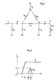
- Figure 1 shows a pulse generator of current injection type according to a first embodiment of this invention. In this figure, reference symbols J11, J12' J2 and J3 denote Josephson junctions having critical currents I11' I12, I2 and I3 respectively; R11, R12' R21, R0 resistors having resistances r11' r12' r21 and r0 respectively; 11 a gate current supply terminal; 12 an input terminal; 13 an output line; and RL a load resistor with a resistance rL. With the pulse generator of this embodiment, an input/output separation function is added to the pulse generation function and an improvement is made on the gain.
- The gate current Ig supplied from the gate
current supply terminal 11 is divided into two paths, a first path consisting of the resistor R11 and the Josephson junction J11 and a second path consisting of the resistor R12 and the Josephson junction J12. With currents Ig1 and Ig2 flowing through the first path and second path, respectively (Ig1 + Ig2 =Ig), the input current Ic injected from theinput terminal 12 flows through the Josephson junctions J2 and J11 into ground. Consequently, into the Josephson junction J11, both the gate current Ig1 and the input current Ic are injected to switch the junction J11 into the voltage state. The current flowing through the Josephson junction J11 is then injected into the Josephson junction J12 through the resistor R21 and the resistors R11, R12 thereby switching the Josephson junction J12 into the voltage state. Accordingly, the gate current Ig is distributed into two paths, a first path consisting of the Josephson junction J2 and the resistor R0 and a second path consisting of the Josephson junction J3, anoutput line 13 and the load resistor RL. If rL is set greater than r0, almost all the gate current Ig flows into the first path, switching the Josephson junction J2 into the voltage state. As a result, the input current Ic flows through the resistor R0 into ground while the gate current Ig flows through the Josephson J3, theoutput line 13 and into the load resistor RL, thereby achieving the separation between the input and output. - When the current flowing through the
output line 13 exceeds the critical current value I3 of the Josephson junction J3, the Josephson junction J3 is switched into the voltage state, interrupting the output current. Therefore, a pulse current is obtained through theoutput line 13. The gate current Ig is distributed according to the resistance values of the four Josephson junctions in the voltage state and flows into ground. - Figure 2 shows an waveform of the output pulse current Iout obtained in a manner described above. The pulse current Iout starts to rise after the elapse of turn-on delay time Ts necessary for the gate circuit in Figure 1 to switch into the voltage state and continues to rise for the duration of a rise time T1 of the gate circuit to the left of the Josephson junction J3. Then the pulse Iout goes down for the duration of a rise time T2 of the Josephson junction J3. Therefore, the pulse width is determined as (T1 + T2). In consideration that the obtainable switching time of the Josephson junction is about 10 picoseconds, the pulse width of 20 picoseconds may be obtained by the above circuit.
- The above pulse generator, if applied with appropriate design rule, will be able to operate correctly over wide operation range. For this purpose, the following design rule is proposed.


- This design rule is based on the control characteristic of the above pulse generator as shown in Figure 3 which shows the control characteristic of the gate circuit (circuit on the left side of the Josephson junction J3 of Figure 1) in the pulse generator with the shaded portion representing the voltage state of the gate circuit. The
line 21 represents the threshold value characteristic for switching the Josephson junction J11 into the voltage state; theline 23 for switching the Josephson junction J12 into the voltage state with the Josephson Junction J11 in the zero-voltage state; theline 24 for switching the Josephson junction J12 after the completion of switching of the Josephson junction J11; theline 22 for switching the Josephson junction J2 after the completion of switching of the Josephson junctions J11, J12. Referring to Figure 3, in order to obtain a wide operation margin, it is appropriate to set the following conditions I11 = I12 = 3/2 I2 for making thelines line 24 inside the shaded portion determined by thelines - The above-mentioned design adequacy will be explained in the following. The currents i11 (= Ig1) and i12 (= Ig2) flowing through the resistors R11 and R12 into the Josephson junctions J11 and J12 are given by


- The input current Ic is injected into the Josephson junction J11 through the Josephson junction J2. Thus, the condition for switching the Josephson junction J11 is given by

- The
line 21 of Figure 3 corresponds to the above equation (3). - Since the allowable maximum gate current is (I11 + I12) under the zero-voltage state condition of the Josephson junctions J11 and J12, the value of the intersection A of the ordinate and the
line 21 of Figure 3 is (I11 + I12). The condition for switching the Josephson junction J2 is given by
- The equation (4) corresponds to the
line 23. - Considering the switching order (J11, then J2) the gate current must be greater than the value of the intersection B of the
lines 
- Apparently from equation (3), the input sensitivity of the gate is given by

- The following condition is required to switch the Josephson junction J12 after the completion of switching the Josephson junction J11:


line 24.
- After the Josephson junction J12 has switched, the gate current is injected into the Josephson junction J2. Assuming r0 « rL, the condition for switching the Josephson junction J2 is given by

- The above equation (11) corresponds to the
line 22. When the minimum value of Ig given by the equation (11) agrees with
- Consequently, we obtain

- The values of the intersection points between the
line 24 and ordinate and ascissa becomes small as the resistance rO increases. This is preferable in the light of operation margin, but, considering the backlash of the input current Tc, it is desirable to limit r0 to a small value. Thus, the minimum allowable value of r0 is the value attained at a contact point between the intersection B and theline 24. - As a result obtained are I = 2/3 Io and I = 2/3 I0. Substituting them into equation (8) under the condition r21 = r11 ≡ r for the convenience of manufacture, we obtain

- More concretely, when the circuit parameters are chosen as follows


- Compared with the pulse generator using a conventional interferometer type gate circuit, the pulse generator according to this invention needs no input line for magnetic coupling with the gate circuit, which in turn reduces the number of integrated circuit fabrication processes. Further, the absence of inductances makes it possible to produce the logic gate in small and is suited for high density integration. It also does not require an additional provision to dampe the resonance because there is no inductance components causing the resonance in this circuit. Moreover, since this circuit does not use a superconductive loop, there is no risk of trapping stray magnetic flux and causing erroneous operation.
- Now, another embodiment is explained in the following which is based on the construction of Figure 1 but capable of further reducing the pulse rise time and the pulse fall time. Figure 4 shows the circuit of this embodiment. The difference from the first embodiment of Figure 1 is that an inductance component LO is connected in series with the resistor R0 connected to the input terminal. The operation of this circuit is detailed below.
- As the input current Ic is supplied from the
input terminal 12, Ic flows through the Josephson junction J2 into the Josephson junction J11. This causes the current flowing through the Josephson junction J11 to inject into the Josephson junction J12 through the resistor R21 and the resistors R11, R12' switching the Josephson junction J12 into the voltage state. On the other hand, the gate current Ig is bisected into two current paths, a first path made up of the Josephson junction J2, the resistor R0 and the inductance L0 and a second path made up of the Josephson junction J3, theoutput line 13 and the load resistor RL. If the inductance L0 is set sufficiently large, the current path consisting of the Josephson junction J2, resistor RO and inductance L0 presents dynamically a large impedance, causing the gate current Ig to flow through the Josephson junction J3 into theoutput line 13. As a result, the current in theoutput line 13 rises during the switching time of the Josephson junction J12. When the current flowing through theoutput line 13 exceeds the critical current value of the Josephson junction J3, the Josephson junction J3 is switched into the voltage state interrupting the output current. Therefore, a pulse current is obtained through theoutput line 13. The gate current Ig flows through the Josephson junction J2, resistor R0 and inductance L0 into ground, switching the Josephson junction J2 into the voltage state. Consequently, the gate current Ig is distributed according to the resistances of the junctions J11, J12, J2, J3 in the voltage state and flows into ground through them. The input current Ic, on the other hand, flows through the resistor R0 and inductance L0 into ground. In this way, the input and output currents are separated. - As explained in the foregoing, the switching order of the Josephson junctions in this circuit is J11, J12, J3 and J2, and the output pulse Iout rises after completion of switching of the Josephson junctions J11 and J12. Thus an overall capacity of the circuit to be charged at that moment is the sum (= 2C) of the capacity (C) of Josephson junctions J11 and J12. However, in the circuit of Figure 1 the sequence of switching is J11, J12, J2 and J3. Therefore, when Iout rises, the capacitances of the Josephson junctions J11, J12 and J2 (each capacity is supposed to be C) which amounts to 3C, 1.5 times the capacity of the circuit shown in Figure 4, have to be charged. Now. the rise time and fall time of the output pulse Iout depend on the time constant CR. Since the capacitance of the circuit of Figure 4 when Iout is produced is 2/3 the capacitance of the circuit of Figure 1, as mentioned above, the pulse obtained with the pulse generator of Figure 4 has shorter rise time and fall time. In this circuit, too, in order to keep the high input sensitivity and wide operation margin, it is preferable that the design rule similar to that of Figure 1 be followed. It is apparent that when the connecting sequence of the resistor R0 and inductance L0 is reversed the same effect can be obtained.
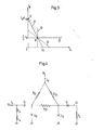
- Figure 5 shows a pulse generator circuit, a still another embodiment of this invention, in which further improvement is made on the operation margin and gain. In this circuit, a resistor R22 (resistance r22) is inserted between the connecting point C or D (between resistors R12 and R21 or between resistors R11 and R21) and the Josephson junction J3 or J2; a resistor R13 (resistance r13) is inserted between the connecting point E (between the resistor R22 and the junction J3) and the connecting point F (between resistors R11 and R12); and a Josephson junction J13 (critical current I13) is added between the connecting point E and the ground.
- The operation margin and the gain are further improved as the number of resistors and Josephson junctions increases. This may be explained as follows.
- As is evident from the explanation for Figure 3, the input sensitivity depends on the gradient of the
threshold line 21 for the Josephson junction J11. If we suppose the added resistors (n pieces including R11 and R12) have resistance equal to that of R11 and R12 and the Josephson junctions (n pieces including J11 and J12) have critical current equal to I11 of J11 and I12 of J12, then the threshold line for theline 21 is expressed as
- Therefore, the greater the number of added resistors and Josephson junctions, the higher the input sensitivity will be.
- Since it holds that Ig > I2 and Ic > I2 for
lines lines 
- That is I2 =

- On the other hand, since


- Equation (17) also shows that the operation margin increases as the number of added resistors and Josephson junctions increases.
- The operation of the circuit as shown in Figure 5 is explained in the following. The gate current Ig is trisected into three current paths, a first path consisting of resistor R11 and Josephson junction J11, a second path consisting of resistor R12 and Josephson junction J12, and a third path consisting of resistor R13 and Josephson junction J13 with Ig1, Ig2 and Ig3, respectively.
- As the input current Ic is injected, it flows through the Josephson junctions J2 and J11 into ground. As a result, both the gate current Ig1 and the input current Ic flow through the Josephson junction J11, switching it into the voltage state. This causes the current flowing through the Josephson junction J11 to inject through the resistor R21 and the resistors R11, R12 into the Josephson junction J12, switching the Josephson junction J12 to the voltage state. Then the current flowing through the junction J12 is injected into the Josephson junction J13 through the resistor R22 and the resistors R12, R13, thereby switching the Josephson junction J13 into the voltage state.
- Consequently, the gate current Ig is bisected into two paths, a first path consisting of Josephson junction J2 and resistor R0 and a second path consisting of Josephson junction J3,
output line 13 and load resistor RL. If the resistance rL of the load resistor RL is set sufficiently higher than the resistance r0 of the resistor R0, most of the gate current Ig flows through the Josephson junction J2 and resistor R0 thus switching the Josephson junction J2 into the voltage state. This:causes the input current Ic to flow through the resistor R0 into ground and the gate current Ig to flow through the Josephson junction J3,output line 13 and load resistor RL and into the ground. In this way, the input and output are separated. - As the current flowing through the
output line 13 exceeds the critical current value I3 of the Josephson junction J3, the Josephson junction J3 is switched into the voltage stage, cutting off the output current. As a result, a pulse current is obtained through theoutput line 13. The gate current Ig is distributed according to the resistance of each junction in the voltage state and flows into ground-through them. - As can be seen from the foregoing, the rise time and fall time of the output pulse current Iout are given by the switching time of the Josephson junctions J2 and J3, respectively. The pulse width is also given as the sum of these switching times.
- Figure 6 shows another embodiment of the present invention in which an inductance component L0 is connected in series with the resistance R0 of Figure 5 to further shorten the output pulse width. The operation of this circuit is similar to that of Figure 1 and Figure 4, so detailed explanation is not presented here. In summary, at the time of switching the Josephson junction J3 from which the output pulse is obtained, the junction J2 is not switched into the voltage state due to the inductance component LO. Therefore the overall capacity of the gate circuit is the sum of each capacity of the Josephson junctions J11, J12 and J13, which is 3/4 the capacity of the circuit of Figure 5. This means the pulse width is further reduced.
- To ensure correct operation of the pulse generator shown in Figures 5 and 6 over wide operation range, it is desirable to follow the design rule, as explained for Figure 1, such as shown below.


Claims (11)


Applications Claiming Priority (4)
| Application Number | Priority Date | Filing Date | Title |
|---|---|---|---|
| JP30317/82 | 1982-02-26 | ||
| JP30316/82 | 1982-02-26 | ||
| JP3031682A JPS58147228A (en) | 1982-02-26 | 1982-02-26 | Current injection type pulse generating circuit using josephson effect |
| JP3031782A JPS58147229A (en) | 1982-02-26 | 1982-02-26 | Current injection type pulse generating circuit using josephson effect |
Publications (2)
| Publication Number | Publication Date |
|---|---|
| EP0087764A1 true EP0087764A1 (en) | 1983-09-07 |
| EP0087764B1 EP0087764B1 (en) | 1986-08-06 |
Family
ID=26368641
Family Applications (1)
| Application Number | Title | Priority Date | Filing Date |
|---|---|---|---|
| EP83101807A Expired EP0087764B1 (en) | 1982-02-26 | 1983-02-24 | Josephson pulse generator of current injection type |
Country Status (3)
| Country | Link |
|---|---|
| US (1) | US4603263A (en) |
| EP (1) | EP0087764B1 (en) |
| DE (1) | DE3365058D1 (en) |
Families Citing this family (4)
| Publication number | Priority date | Publication date | Assignee | Title |
|---|---|---|---|---|
| US5266844A (en) * | 1991-07-15 | 1993-11-30 | Hewlett-Packard Company | Timing discriminator circuit and method for determining the arrival order of input signals |
| US5233243A (en) * | 1991-08-14 | 1993-08-03 | Westinghouse Electric Corp. | Superconducting push-pull flux quantum logic circuits |
| US5331297A (en) * | 1991-12-26 | 1994-07-19 | Kyocera Corporation | Josephson device a.c. power supply circuit and circuit substrate for mounting same |
| US5552735A (en) * | 1994-10-07 | 1996-09-03 | Northrop Grumman Corporation | Multi-gigahertz single flux quantum switch |
Citations (2)
| Publication number | Priority date | Publication date | Assignee | Title |
|---|---|---|---|---|
| US4275314A (en) * | 1979-04-30 | 1981-06-23 | Bell Telephone Laboratories, Incorporated | Josephson Atto-Weber switch |
| GB2078046A (en) * | 1980-06-10 | 1981-12-23 | Nippon Telegraph & Telephone | Superconductive logic circuit |
Family Cites Families (2)
| Publication number | Priority date | Publication date | Assignee | Title |
|---|---|---|---|---|
| US4313066A (en) * | 1979-08-20 | 1982-01-26 | International Business Machines Corporation | Direct coupled nonlinear injection Josephson logic circuits |
| JPS5846727A (en) * | 1981-09-14 | 1983-03-18 | Nec Corp | Current injection type logical gate circuit using josephson effect |
-
1983
- 1983-02-23 US US06/468,908 patent/US4603263A/en not_active Expired - Fee Related
- 1983-02-24 EP EP83101807A patent/EP0087764B1/en not_active Expired
- 1983-02-24 DE DE8383101807T patent/DE3365058D1/en not_active Expired
Patent Citations (2)
| Publication number | Priority date | Publication date | Assignee | Title |
|---|---|---|---|---|
| US4275314A (en) * | 1979-04-30 | 1981-06-23 | Bell Telephone Laboratories, Incorporated | Josephson Atto-Weber switch |
| GB2078046A (en) * | 1980-06-10 | 1981-12-23 | Nippon Telegraph & Telephone | Superconductive logic circuit |
Non-Patent Citations (4)
| Title |
|---|
| APPLIED PHYSICS LETTERS, vol. 36, no. 12, June 1980, New York D.B. TUCKERMAN "A Josephson ultrahigh-resolution sampling system", pages 1008-1010 * |
| IBM TECHNICAL DISCLOSURE BULLETIN, vol. 22, no. 2, July 1979 S.M. FARIS et al. "Pulsed output star driver", pages 846-847 * |
| IBM TECHNICAL DISCLOSURE BULLETIN, vol. 25, no. 3A, August 1982 S.M. FARIS et al. "Isolator for Josephson Logic", pages 1207-1208 * |
| IEEE TRANSACTIONS ON ELECTRON DEVICES, vol. ED-27, no. 10, October 1980 T.R. GHEEWALA "Josephson-logic devices and circuits", pages 1857-1869 * |
Also Published As
| Publication number | Publication date |
|---|---|
| US4603263A (en) | 1986-07-29 |
| DE3365058D1 (en) | 1986-09-11 |
| EP0087764B1 (en) | 1986-08-06 |
Similar Documents
| Publication | Publication Date | Title |
|---|---|---|
| US6549059B1 (en) | Underdamped Josephson transmission line | |
| US4678942A (en) | Emitter coupled logic circuit with high drivability for capacitive load | |
| Gheewala | Josephson-logic devices and circuits | |
| EP0074666B1 (en) | Circuit utilizing josephson effect | |
| EP0087764A1 (en) | Josephson pulse generator of current injection type | |
| US2909680A (en) | Conditional steering gate for a complementing flip flop | |
| US5124583A (en) | Dc-powered josephson integrated circuit | |
| EP0069534B1 (en) | Superconducting logic circuit | |
| EP0066239B1 (en) | Pulse generation circuit using at least one josephson junction device | |
| US4373138A (en) | Hybrid unlatching flip-flop logic element | |
| CA1189916A (en) | Circuit utilizing josephson effect | |
| JPH0230209B2 (en) | ||
| Pei | Logic delays of 5‐μm current‐switched Josephson gates | |
| JPH0425639B2 (en) | ||
| Haynes | Logic circuits using square-loop magnetic devices: a survey | |
| US3487235A (en) | Floating tunnel diode hybrid latch | |
| KR830002524B1 (en) | Binary divider integrated circuit | |
| JP2778245B2 (en) | Josephson drive circuit with polarity switching | |
| JPH0374053B2 (en) | ||
| Eldridge | A new high-speed digital technique for computer use | |
| JPH0425640B2 (en) | ||
| JPH0374051B2 (en) | ||
| JPS58146125A (en) | Current injection type pulse generating circuit using josephson effect | |
| US6654312B1 (en) | Method of forming a low voltage semiconductor storage device and structure therefor | |
| JPS59123310A (en) | Timing pulse generating circuit |
Legal Events
| Date | Code | Title | Description |
|---|---|---|---|
| PUAI | Public reference made under article 153(3) epc to a published international application that has entered the european phase |
Free format text: ORIGINAL CODE: 0009012 |
|
| AK | Designated contracting states |
Designated state(s): DE FR GB IT NL |
|
| RAP1 | Party data changed (applicant data changed or rights of an application transferred) |
Owner name: NEC CORPORATION |
|
| 17P | Request for examination filed |
Effective date: 19831222 |
|
| GRAA | (expected) grant |
Free format text: ORIGINAL CODE: 0009210 |
|
| AK | Designated contracting states |
Kind code of ref document: B1 Designated state(s): DE FR GB IT NL |
|
| REF | Corresponds to: |
Ref document number: 3365058 Country of ref document: DE Date of ref document: 19860911 |
|
| ET | Fr: translation filed | ||
| ITF | It: translation for a ep patent filed |
Owner name: MODIANO & ASSOCIATI S.R.L. |
|
| PLBE | No opposition filed within time limit |
Free format text: ORIGINAL CODE: 0009261 |
|
| STAA | Information on the status of an ep patent application or granted ep patent |
Free format text: STATUS: NO OPPOSITION FILED WITHIN TIME LIMIT |
|
| 26N | No opposition filed | ||
| ITTA | It: last paid annual fee | ||
| PGFP | Annual fee paid to national office [announced via postgrant information from national office to epo] |
Ref country code: FR Payment date: 19950217 Year of fee payment: 13 |
|
| PGFP | Annual fee paid to national office [announced via postgrant information from national office to epo] |
Ref country code: GB Payment date: 19950222 Year of fee payment: 13 |
|
| PGFP | Annual fee paid to national office [announced via postgrant information from national office to epo] |
Ref country code: NL Payment date: 19950228 Year of fee payment: 13 |
|
| PG25 | Lapsed in a contracting state [announced via postgrant information from national office to epo] |
Ref country code: GB Effective date: 19960224 |
|
| PGFP | Annual fee paid to national office [announced via postgrant information from national office to epo] |
Ref country code: DE Payment date: 19960422 Year of fee payment: 14 |
|
| PG25 | Lapsed in a contracting state [announced via postgrant information from national office to epo] |
Ref country code: NL Effective date: 19960901 |
|
| GBPC | Gb: european patent ceased through non-payment of renewal fee |
Effective date: 19960224 |
|
| PG25 | Lapsed in a contracting state [announced via postgrant information from national office to epo] |
Ref country code: FR Effective date: 19961031 |
|
| NLV4 | Nl: lapsed or anulled due to non-payment of the annual fee |
Effective date: 19960901 |
|
| REG | Reference to a national code |
Ref country code: FR Ref legal event code: ST |
|
| PG25 | Lapsed in a contracting state [announced via postgrant information from national office to epo] |
Ref country code: DE Effective date: 19971101 |