EP0086397A2 - Differential current distributing circuit - Google Patents
Differential current distributing circuit Download PDFInfo
- Publication number
- EP0086397A2 EP0086397A2 EP83100936A EP83100936A EP0086397A2 EP 0086397 A2 EP0086397 A2 EP 0086397A2 EP 83100936 A EP83100936 A EP 83100936A EP 83100936 A EP83100936 A EP 83100936A EP 0086397 A2 EP0086397 A2 EP 0086397A2
- Authority
- EP
- European Patent Office
- Prior art keywords
- current
- transistor
- output terminal
- path
- input signal
- Prior art date
- Legal status (The legal status is an assumption and is not a legal conclusion. Google has not performed a legal analysis and makes no representation as to the accuracy of the status listed.)
- Granted
Links
Images

Classifications
-
- H—ELECTRICITY
- H02—GENERATION; CONVERSION OR DISTRIBUTION OF ELECTRIC POWER
- H02P—CONTROL OR REGULATION OF ELECTRIC MOTORS, ELECTRIC GENERATORS OR DYNAMO-ELECTRIC CONVERTERS; CONTROLLING TRANSFORMERS, REACTORS OR CHOKE COILS
- H02P6/00—Arrangements for controlling synchronous motors or other dynamo-electric motors using electronic commutation dependent on the rotor position; Electronic commutators therefor
- H02P6/08—Arrangements for controlling the speed or torque of a single motor
-
- H—ELECTRICITY
- H02—GENERATION; CONVERSION OR DISTRIBUTION OF ELECTRIC POWER
- H02P—CONTROL OR REGULATION OF ELECTRIC MOTORS, ELECTRIC GENERATORS OR DYNAMO-ELECTRIC CONVERTERS; CONTROLLING TRANSFORMERS, REACTORS OR CHOKE COILS
- H02P6/00—Arrangements for controlling synchronous motors or other dynamo-electric motors using electronic commutation dependent on the rotor position; Electronic commutators therefor
- H02P6/28—Arrangements for controlling current
Definitions
- This invention relates to a differential current distributing circuit.
- a hall motor for example, at least one hall element is arranged around a rotor having an alternate array of N and S poles so as to detect the momentary position of the rotor.
- a drive current for driving the rotor is supplied to one of at least two driving coils disposed around the rotor by using the detection signal from the hall element, causing the rotor to be rotated in a predetermined direction.
- Fig. 1 shows a conventional differential current distributing circuit which can be used for this purpose.
- An emitter-collector path of a transistor TR1 of a predetermined conductivity type, for example, a PNP type is connected between an output terminal of a constant current source IE and a first current output terminal 1.
- a transistor TR2 of the same conductivity type as the transistor TR1 is connected between the output terminal of the constant current source IE and a second current output terminal 2.
- a signal INl on one output terminal of the hall element is coupled to the base electrode of the transistor TR1 and a signal IN2 on the other output terminal of the hall element is coupled to the base electrode of the transistor TR2.
- Fig. 2 shows the characteristic curve of the differential current distributing circuit as shown in Fig. 1.
- the abscissa in Fig. 2 denotes the polarity and level of the input signal INl with the input signal IN2 as a reference.
- a "0" point on the abscissa is a point where the level of the input signal INl is equal to that of the input signal IN2.
- FIG. 2 shows the direction in which the input signal INl is positive with respect to the input signal IN2 and the arrow 4 in Fig. 2 shows the direction in which the input signal IN1 is negative with respect to the input signal IN2.
- the ordinate in Fig. 2 shows the amplitude of the distributed current.
- I 1 denotes a current value as obtained from the current output terminal 1 and 1 2 a current value as obtained from the current output terminal 2.
- I 11 shows the value of the current I 1 when the input signal IN1 has a negative value corresponding to a line 0-5 with respect to the input signal IN2, and I 21 shows the value of the current 1 2 under the same conditions.
- the current I 1 is supplied to one drive coil for the rotor and the current 1 2 is supplied to the other drive coil for the rotor.
- the polarities of the output signals of the hall element, i.e., the input signals IN1 and IN2 to the current distributing circuit vary according to the rotation of the rotor. It is desirable that the output current of the constant current source IE be completely and accurately distributed into one drive coil or the other drive coil in response to the point of time at which the polarity of the input signal IN1 or IN2 varies from positive to negative or from negative to positive. As evident from Fig.
- the current I 1 and current 1 2 vary along a hyperbolic tangential curve corresponding to the level of the input signal IN1 with the input signal IN2 as a reference. Therefore, it is difficult to completely distribute the current I from the constant current source IE into either of the current output terminals 1 and 2 in sharp response to the time at which the polarity of the input signal varies.
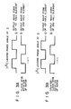
- a denotes the output waveform of the first hall element
- b denotes the output waveform of the second hall element
- the output waveform b is lagged by an angle 6 with respect to the output waveform a.
- the polarity of the waveform a is opposite to that of the waveform b (Fig. 3A).
- the waveform b When the rotor is rotated in the counterclockwise direction, the waveform b is leaded by the angle e with respect to the waveform a and at the rise of the output waveform a the waveforms a and b have the same polarity. In other words, at the rise of the output waveform a of the first hall element the polarity of the output waveform a is different from that of the output waveform b of the second hall element if the rotational direction of the rotor is different. It is to be noted that a first differential current distributing circuit is connected to the output ends of the first hall element and that a second differential current distributing circuit is connected to the output ends of the second hall element.
- the rotation direction of the rotor is detected by the outputs of the two hall elements and, when the distribution of the current is to be effected in the first current distributing circuit, the value of the output current I of the constant current source IE in the first current distributing circuit is varied by the output of the second hall element according to the result of the detection.
- the current distributing circuit have the following characteristic. That is, it is desired that, according to the polarity of that input signal IN1 with respect to the input signal IN2 which corresponds to the instant at which the current of the current source IE begins to flow, the output current of the current source IE be completely distributed into either of the first current path including the first current output terminal 1 and second current path including the second current output terminal 2, and that, even if the polarity of the input signal INl varies with respect to the input signal IN2, the distributed current path remain established during the time period in which the current of the current source IE maintains a predetermined level.
- a differential current distributing circuit comprising a constant current source; a first current path including a first resistor, collector-emitter path of a first transistor of first conductivity type and emitter-collector path of a second transistor of second conductivity type which are connected in series between an output terminal of the constant current source and a first current output terminal; and a second current path including a second resistor, collector-emitter path of a third transistor of first conductivity type and emitter-collector path of a fourth transistor of second conductivity type which are connected in series between the output terminal of the constant current source and a second current output terminal; in which the base electrode of the first transistor is connected to the output terminal of the second resistor, the base electrode of the third transistor is connected to the output terminal of the first resistor, a first input signal is supplied to the base electrode of the second transistor, a second input signal is supplied to the base electrode of the fourth transistor, and an output current of the constant current source is distributed into either of the first and second current paths according to a level difference
- FIG. 4 shows the same reference numeals are employed to designate parts or elements corresponding to those as shown in Fig. 1.
- reference symbol I shows the output current of a constant current source IE.
- a first current path comprising a series circuit of a first resistor Rl having a predetermined resistive value, collector-emitter path of a first transistor TR3 of npn type and emitter-collector path of a second transistor TR1 of pnp type is connected between the constant current source IE and a first current output terminal 1.
- a second current path comprising a series circuit of a second resistor R2 having the same resistive value as that of the resistor Rl, collector-emitter path of a third transistor TR4 of npn type having the same characteristic as that of the transistor TR3 and emitter-collector path of a fourth transistor of a pnp type having the same characteristic as that of the transistor TR1 is connected between the output terminal of the constant current source IE and a second current output terminal 2.
- the base electrode of the first transistor TR3 is connected to the output terminal of the second resistor R2 and the base electrode of the third transistor TR4 is connected to the output terminal of the first resistor Rl.
- a first input signal INl is supplied to the base electrode of the second transistor TR1 and a second input signal IN2 is supplied to the base electrode of the fourth transistor TR2.
- a signal on one terminal of an output circuit of a hall element arranged around the rotor of a hall motor is supplied as a first input signal INl and a signal on the other terminal of the output circuit is supplied as a second input signal IN2.
- the current of the small value flows through a third current path comprising the first resistor Rl, base-emitter path of the third transistor TR4 and emitter-collector path of the fourth transistor TR2, and through a fourth current path comprising the second resistor R2, base-emitter path of the first transistor TR3 and emitter-collector path of the second transistor TR1.
- more current flows through either of the third or the fourth current path depending upon which of the input signals INl or IN2 has a lower voltage level.
- the input signal IN1 has a lower voltage level than that of the input signal IN2
- more current flows through the fourth current path than through the third current path.
- the current through the fourth current path is supplied to the base of the first transistor TR3, causing a resistive value of the collector-emitter path of the first transistor TR3 to be lowered and the collector current of the transistor TR3 to be increased. Then, the base current of the third transistor TR4 is decreased due to a voltage drop across the first resistor Rl. In this way, the base current of the transistor TR4 is gradually further decreased, cutting off the third and fourth transistors TR4 and TR2. Even if the level of the first input signal IN1 becomes greater than that of the input signal IN2 during the cut-off period of the transistors TR4 and TR2, the above-mentioned current distribution is maintained so long as the input voltage to the base electrode of the transistor TR4 is smaller than a predetermined voltage level.
- the predetermined input voltage level means an input voltage to the base electrode of the transistor TR4 when the collector current of the transistor TR3 is decreased, the voltage across the first resistor Rl drops down to 0.6 V and the cut-off of the transistor TR4 is released.
- the level of the input signal IN2 is lower than that of the input signal IN1
- more current flows through the third current path than the fourth current path.
- the output current I of the constant current source IE is distributed into the second current path as indicated by 1 2 in Fig. 4. That is, the transistors TR3 and TR1 are cut-off and the output current I of the constant current source IE is distributed into the second current path.
- the current 12 remains distributed through the second current path until the voltage across the second resistor R2 drops down to 0.6 V to cause the cut-off of the transistor TR3 to be released.
- the current I from the constant current source IE is completely distributed into either of the first and the second current path according to a level difference between the input signals IN1 and IN2 which corresponds to the instant at which the output current I of the constant current source IE begins to increase from a substantially zero level.
- the differential current distributing circuit according to this invention even if the polarities of the input signals INl and IN2 vary, the current path through which the current is once distributed remains established so long as the current so distributed is maintained at a predetermined level.
- the application of the differential current distributing circuit as shown in Fig. 4 is not limited to a drive circuit for a hall motor.
Abstract
Description
- This invention relates to a differential current distributing circuit.
- In a known hall motor, for example, at least one hall element is arranged around a rotor having an alternate array of N and S poles so as to detect the momentary position of the rotor. A drive current for driving the rotor is supplied to one of at least two driving coils disposed around the rotor by using the detection signal from the hall element, causing the rotor to be rotated in a predetermined direction. Fig. 1 shows a conventional differential current distributing circuit which can be used for this purpose. An emitter-collector path of a transistor TR1 of a predetermined conductivity type, for example, a PNP type is connected between an output terminal of a constant current source IE and a first
current output terminal 1. A transistor TR2 of the same conductivity type as the transistor TR1 is connected between the output terminal of the constant current source IE and a secondcurrent output terminal 2. A signal INl on one output terminal of the hall element is coupled to the base electrode of the transistor TR1 and a signal IN2 on the other output terminal of the hall element is coupled to the base electrode of the transistor TR2. Fig. 2 shows the characteristic curve of the differential current distributing circuit as shown in Fig. 1. The abscissa in Fig. 2 denotes the polarity and level of the input signal INl with the input signal IN2 as a reference. A "0" point on the abscissa is a point where the level of the input signal INl is equal to that of the input signal IN2. Thearrow 3 in Fig. 2 shows the direction in which the input signal INl is positive with respect to the input signal IN2 and thearrow 4 in Fig. 2 shows the direction in which the input signal IN1 is negative with respect to the input signal IN2. The ordinate in Fig. 2 shows the amplitude of the distributed current. In the graph as shown in Fig. 2, I1 denotes a current value as obtained from thecurrent output terminal 1 and 12 a current value as obtained from thecurrent output terminal 2. In Fig. 2, I11 shows the value of the current I1 when the input signal IN1 has a negative value corresponding to a line 0-5 with respect to the input signal IN2, and I21 shows the value of the current 12 under the same conditions. When the current distributing circuit as shown in Fig. 1, is used as the drive circuit for the hall motor, the current I1 is supplied to one drive coil for the rotor and the current 12 is supplied to the other drive coil for the rotor. The polarities of the output signals of the hall element, i.e., the input signals IN1 and IN2 to the current distributing circuit vary according to the rotation of the rotor. It is desirable that the output current of the constant current source IE be completely and accurately distributed into one drive coil or the other drive coil in response to the point of time at which the polarity of the input signal IN1 or IN2 varies from positive to negative or from negative to positive. As evident from Fig. 2, the current I1 and current 12 vary along a hyperbolic tangential curve corresponding to the level of the input signal IN1 with the input signal IN2 as a reference. Therefore, it is difficult to completely distribute the current I from the constant current source IE into either of thecurrent output terminals - There is the case where it is desired to detect the rotational direction of the rotor by a means (not shown) and to control the driving of the hall motor by the detection signal from a hall element. In this case, a plurality of hall elements are arranged around the rotor. The respective hall element produces an output signal corresponding to the rotational position of the rotor. The hall elements can be arranged such that the cycles of the position signals from the respective hall elements have the same cycle, but that the phases of the position signals are different from each other.
- The reason whey the rotational direction of the rotor can be detected by arranging, for example, two hall elements around the rotor will be explained below by referring to Figs. 3A and 3B. Now suppose that in Fig. 3A a denotes the output waveform of the first hall element, that b denotes the output waveform of the second hall element and that when the rotor is rotated in the clockwise direction the output waveform b is lagged by an angle 6 with respect to the output waveform a. At the rise of the waveform a the polarity of the waveform a is opposite to that of the waveform b (Fig. 3A). When the rotor is rotated in the counterclockwise direction, the waveform b is leaded by the angle e with respect to the waveform a and at the rise of the output waveform a the waveforms a and b have the same polarity. In other words, at the rise of the output waveform a of the first hall element the polarity of the output waveform a is different from that of the output waveform b of the second hall element if the rotational direction of the rotor is different. It is to be noted that a first differential current distributing circuit is connected to the output ends of the first hall element and that a second differential current distributing circuit is connected to the output ends of the second hall element. The rotation direction of the rotor is detected by the outputs of the two hall elements and, when the distribution of the current is to be effected in the first current distributing circuit, the value of the output current I of the constant current source IE in the first current distributing circuit is varied by the output of the second hall element according to the result of the detection.
- In such a case, it is desired that the current distributing circuit have the following characteristic. That is, it is desired that, according to the polarity of that input signal IN1 with respect to the input signal IN2 which corresponds to the instant at which the current of the current source IE begins to flow, the output current of the current source IE be completely distributed into either of the first current path including the first
current output terminal 1 and second current path including the secondcurrent output terminal 2, and that, even if the polarity of the input signal INl varies with respect to the input signal IN2, the distributed current path remain established during the time period in which the current of the current source IE maintains a predetermined level. - Since, however, the current values I1 and 12 obtained from the output
current terminals - It is accordingly the object of this invention to provide a differential current distributing circuit in which the current of a constant current source can be completely distributed into one of first and second current paths in sharp response to a change in the polarity of an input signal and the current path so distributed remains established even if the polarity of the input signal varies.
- According to this invention there is provided a differential current distributing circuit comprising a constant current source; a first current path including a first resistor, collector-emitter path of a first transistor of first conductivity type and emitter-collector path of a second transistor of second conductivity type which are connected in series between an output terminal of the constant current source and a first current output terminal; and a second current path including a second resistor, collector-emitter path of a third transistor of first conductivity type and emitter-collector path of a fourth transistor of second conductivity type which are connected in series between the output terminal of the constant current source and a second current output terminal; in which the base electrode of the first transistor is connected to the output terminal of the second resistor, the base electrode of the third transistor is connected to the output terminal of the first resistor, a first input signal is supplied to the base electrode of the second transistor, a second input signal is supplied to the base electrode of the fourth transistor, and an output current of the constant current source is distributed into either of the first and second current paths according to a level difference between the first and second input signals.
- This invention can be more fully understood from the following detailed description when taken in conjunction with the accompanying drawings, in which:
- Fig. 1 is a circuit diagram showing a conventional differential current distributing circuit;
- Fig. 2 is a characteristic curve showing the amplitude of the distributed current of the circuit as shown in Fig. 1;
- Figs. 3A and 3B show waveforms of the output signals of hall elements for explaining the detection of the rotational direction of a hall motor;
- Fig. 4 is a circuit diagram showing a differential current distributing circuit of this invention; and
- Fig. 5 is a characteristic curve showing the amplitude of the distributed current of the circuit of Fig. 4.
- In Fig. 4, the same reference numeals are employed to designate parts or elements corresponding to those as shown in Fig. 1. In Fig. 4, reference symbol I shows the output current of a constant current source IE. A first current path comprising a series circuit of a first resistor Rl having a predetermined resistive value, collector-emitter path of a first transistor TR3 of npn type and emitter-collector path of a second transistor TR1 of pnp type is connected between the constant current source IE and a first
current output terminal 1. A second current path comprising a series circuit of a second resistor R2 having the same resistive value as that of the resistor Rl, collector-emitter path of a third transistor TR4 of npn type having the same characteristic as that of the transistor TR3 and emitter-collector path of a fourth transistor of a pnp type having the same characteristic as that of the transistor TR1 is connected between the output terminal of the constant current source IE and a secondcurrent output terminal 2. The base electrode of the first transistor TR3 is connected to the output terminal of the second resistor R2 and the base electrode of the third transistor TR4 is connected to the output terminal of the first resistor Rl. A first input signal INl is supplied to the base electrode of the second transistor TR1 and a second input signal IN2 is supplied to the base electrode of the fourth transistor TR2. - The operation of the differential current distributing circuit of Fig. 4 will be explained below by referring to Fig. 5. Now suppose that a signal on one terminal of an output circuit of a hall element arranged around the rotor of a hall motor is supplied as a first input signal INl and a signal on the other terminal of the output circuit is supplied as a second input signal IN2. When the output current I from the constant current source IE begins to increase from a small value which is substantially zero, the current of the small value flows through a third current path comprising the first resistor Rl, base-emitter path of the third transistor TR4 and emitter-collector path of the fourth transistor TR2, and through a fourth current path comprising the second resistor R2, base-emitter path of the first transistor TR3 and emitter-collector path of the second transistor TR1. In this case, more current flows through either of the third or the fourth current path depending upon which of the input signals INl or IN2 has a lower voltage level. When, for example, the input signal IN1 has a lower voltage level than that of the input signal IN2, more current flows through the fourth current path than through the third current path. The current through the fourth current path is supplied to the base of the first transistor TR3, causing a resistive value of the collector-emitter path of the first transistor TR3 to be lowered and the collector current of the transistor TR3 to be increased. Then, the base current of the third transistor TR4 is decreased due to a voltage drop across the first resistor Rl. In this way, the base current of the transistor TR4 is gradually further decreased, cutting off the third and fourth transistors TR4 and TR2. Even if the level of the first input signal IN1 becomes greater than that of the input signal IN2 during the cut-off period of the transistors TR4 and TR2, the above-mentioned current distribution is maintained so long as the input voltage to the base electrode of the transistor TR4 is smaller than a predetermined voltage level. The predetermined input voltage level means an input voltage to the base electrode of the transistor TR4 when the collector current of the transistor TR3 is decreased, the voltage across the first resistor Rl drops down to 0.6 V and the cut-off of the transistor TR4 is released. When the level of the input signal IN2 is lower than that of the input signal IN1, more current flows through the third current path than the fourth current path. As a result, the output current I of the constant current source IE is distributed into the second current path as indicated by 12 in Fig. 4. That is, the transistors TR3 and TR1 are cut-off and the output current I of the constant current source IE is distributed into the second current path. Even if the level of the input signal IN2 becomes higher than that of the input signal INl, the current 12 remains distributed through the second current path until the voltage across the second resistor R2 drops down to 0.6 V to cause the cut-off of the transistor TR3 to be released.
- As mentioned above, the current I from the constant current source IE is completely distributed into either of the first and the second current path according to a level difference between the input signals IN1 and IN2 which corresponds to the instant at which the output current I of the constant current source IE begins to increase from a substantially zero level. Further, the differential current distributing circuit according to this invention, even if the polarities of the input signals INl and IN2 vary, the current path through which the current is once distributed remains established so long as the current so distributed is maintained at a predetermined level.
- The application of the differential current distributing circuit as shown in Fig. 4 is not limited to a drive circuit for a hall motor.
Claims (1)
Applications Claiming Priority (2)
| Application Number | Priority Date | Filing Date | Title |
|---|---|---|---|
| JP20817/82 | 1982-02-12 | ||
| JP57020817A JPS58138111A (en) | 1982-02-12 | 1982-02-12 | Differential detection circuit |
Publications (3)
| Publication Number | Publication Date |
|---|---|
| EP0086397A2 true EP0086397A2 (en) | 1983-08-24 |
| EP0086397A3 EP0086397A3 (en) | 1984-04-11 |
| EP0086397B1 EP0086397B1 (en) | 1986-08-13 |
Family
ID=12037579
Family Applications (1)
| Application Number | Title | Priority Date | Filing Date |
|---|---|---|---|
| EP83100936A Expired EP0086397B1 (en) | 1982-02-12 | 1983-02-01 | Differential current distributing circuit |
Country Status (4)
| Country | Link |
|---|---|
| US (1) | US4506170A (en) |
| EP (1) | EP0086397B1 (en) |
| JP (1) | JPS58138111A (en) |
| DE (1) | DE3365203D1 (en) |
Cited By (4)
| Publication number | Priority date | Publication date | Assignee | Title |
|---|---|---|---|---|
| EP0424390B1 (en) * | 1989-04-01 | 1993-12-29 | Alcatel N.V. | Voltage comparator |
| WO2017127572A1 (en) | 2016-01-21 | 2017-07-27 | 3M Innovative Properties Company | Additive processing of fluoropolymers |
| WO2019016738A2 (en) | 2017-07-19 | 2019-01-24 | 3M Innovative Properties Company | Method of making polymer articles and polymer composites by additive processing and polymer and composite articles |
| WO2019016739A2 (en) | 2017-07-19 | 2019-01-24 | 3M Innovative Properties Company | Additive processing of fluoropolymers |
Families Citing this family (4)
| Publication number | Priority date | Publication date | Assignee | Title |
|---|---|---|---|---|
| US4622475A (en) * | 1984-03-05 | 1986-11-11 | Tektronix, Inc. | Data storage element having input and output ports isolated from regenerative circuit |
| JPS6392109A (en) * | 1986-10-07 | 1988-04-22 | Toshiba Corp | Differential amplifier circuit |
| US4760286A (en) * | 1987-07-20 | 1988-07-26 | Motorola, Inc. | Comparator with input offset current elimination |
| JPH06101671B2 (en) * | 1989-09-27 | 1994-12-12 | 株式会社東芝 | Voltage comparison circuit |
Citations (3)
| Publication number | Priority date | Publication date | Assignee | Title |
|---|---|---|---|---|
| US3938014A (en) * | 1973-02-16 | 1976-02-10 | Fuji Electric Co., Ltd. | Brushless d-c motor |
| DE2905629B2 (en) * | 1978-02-15 | 1981-02-26 | Hitachi, Ltd., Tokio | Differential amplifier |
| GB2077542A (en) * | 1980-06-02 | 1981-12-16 | Philips Nv | Amplifier with negligible dc response |
Family Cites Families (2)
| Publication number | Priority date | Publication date | Assignee | Title |
|---|---|---|---|---|
| US3848139A (en) * | 1973-09-14 | 1974-11-12 | Fairchild Camera Instr Co | High-gain comparator circuit |
| DE2751881A1 (en) * | 1977-11-21 | 1979-05-23 | Siemens Ag | MONOLITHIC DIGITAL SEMI-CONDUCTOR CIRCUIT WITH SEVERAL BIPOLAR TRANSISTORS |
-
1982
- 1982-02-12 JP JP57020817A patent/JPS58138111A/en active Pending
-
1983
- 1983-02-01 DE DE8383100936T patent/DE3365203D1/en not_active Expired
- 1983-02-01 EP EP83100936A patent/EP0086397B1/en not_active Expired
- 1983-02-08 US US06/465,035 patent/US4506170A/en not_active Expired - Lifetime
Patent Citations (3)
| Publication number | Priority date | Publication date | Assignee | Title |
|---|---|---|---|---|
| US3938014A (en) * | 1973-02-16 | 1976-02-10 | Fuji Electric Co., Ltd. | Brushless d-c motor |
| DE2905629B2 (en) * | 1978-02-15 | 1981-02-26 | Hitachi, Ltd., Tokio | Differential amplifier |
| GB2077542A (en) * | 1980-06-02 | 1981-12-16 | Philips Nv | Amplifier with negligible dc response |
Cited By (10)
| Publication number | Priority date | Publication date | Assignee | Title |
|---|---|---|---|---|
| EP0424390B1 (en) * | 1989-04-01 | 1993-12-29 | Alcatel N.V. | Voltage comparator |
| WO2017127572A1 (en) | 2016-01-21 | 2017-07-27 | 3M Innovative Properties Company | Additive processing of fluoropolymers |
| WO2017127561A1 (en) | 2016-01-21 | 2017-07-27 | 3M Innovative Properties Company | Additive processing of fluoropolymers |
| WO2017127569A1 (en) | 2016-01-21 | 2017-07-27 | 3M Innovative Properties Company | Additive processing of fluoroelastomers |
| US11148361B2 (en) | 2016-01-21 | 2021-10-19 | 3M Innovative Properties Company | Additive processing of fluoroelastomers |
| US11179886B2 (en) | 2016-01-21 | 2021-11-23 | 3M Innovative Properties Company | Additive processing of fluoropolymers |
| US11230053B2 (en) | 2016-01-21 | 2022-01-25 | 3M Innovative Properties Company | Additive processing of fluoropolymers |
| WO2019016738A2 (en) | 2017-07-19 | 2019-01-24 | 3M Innovative Properties Company | Method of making polymer articles and polymer composites by additive processing and polymer and composite articles |
| WO2019016739A2 (en) | 2017-07-19 | 2019-01-24 | 3M Innovative Properties Company | Additive processing of fluoropolymers |
| US11760008B2 (en) | 2017-07-19 | 2023-09-19 | 3M Innovative Properties Company | Additive processing of fluoropolymers |
Also Published As
| Publication number | Publication date |
|---|---|
| DE3365203D1 (en) | 1986-09-18 |
| EP0086397B1 (en) | 1986-08-13 |
| JPS58138111A (en) | 1983-08-16 |
| EP0086397A3 (en) | 1984-04-11 |
| US4506170A (en) | 1985-03-19 |
Similar Documents
| Publication | Publication Date | Title |
|---|---|---|
| US3942083A (en) | Brushless motor | |
| EP0086397B1 (en) | Differential current distributing circuit | |
| US4072870A (en) | Comparison circuit having programmable hysteresis | |
| EP0084722A1 (en) | Differential circuit | |
| US3946292A (en) | Brushless motor driving system | |
| GB1563015A (en) | Stator winding drive circuit for brushless dc motor | |
| US4039911A (en) | Dc motor controlled by hall generator | |
| US4338551A (en) | Two-phase brushless motor driving circuit | |
| KR870001558B1 (en) | Dc commtatoress motor | |
| US4072907A (en) | Amplifier circuit | |
| US4511828A (en) | D.C. commutatorless electric motor | |
| EP0098155B1 (en) | Schmitt trigger circuit | |
| US3671837A (en) | Rotation control circuit for transistor motor | |
| US4737696A (en) | Actuator drive circuit | |
| JPH0343866B2 (en) | ||
| EP0089415B1 (en) | Apparatus for measuring flow velocity | |
| US3388307A (en) | Motor load limiting circuitry | |
| JPH0554072B2 (en) | ||
| US5854572A (en) | Compact structure of automatic gain control circuit | |
| JPH0824310B2 (en) | Data signal correction circuit | |
| JP2684062B2 (en) | Sensor abnormality detection circuit | |
| SE452682B (en) | BRIDGE CONNECTOR FINAL STEP FOR AN AUDIO AMPLIFIER | |
| JPH0666648B2 (en) | Hysteresis comparator | |
| SE446798B (en) | AMPLIFIER FOR USE IN A SUBSCRIBER LINE CIRCUIT | |
| JPH0640479Y2 (en) | Current detection circuit |
Legal Events
| Date | Code | Title | Description |
|---|---|---|---|
| PUAI | Public reference made under article 153(3) epc to a published international application that has entered the european phase |
Free format text: ORIGINAL CODE: 0009012 |
|
| PUAI | Public reference made under article 153(3) epc to a published international application that has entered the european phase |
Free format text: ORIGINAL CODE: 0009012 |
|
| 17P | Request for examination filed |
Effective date: 19830225 |
|
| AK | Designated contracting states |
Designated state(s): DE FR GB |
|
| PUAL | Search report despatched |
Free format text: ORIGINAL CODE: 0009013 |
|
| AK | Designated contracting states |
Designated state(s): DE FR GB |
|
| RAP1 | Party data changed (applicant data changed or rights of an application transferred) |
Owner name: KABUSHIKI KAISHA TOSHIBA |
|
| GRAA | (expected) grant |
Free format text: ORIGINAL CODE: 0009210 |
|
| AK | Designated contracting states |
Kind code of ref document: B1 Designated state(s): DE FR GB |
|
| ET | Fr: translation filed | ||
| REF | Corresponds to: |
Ref document number: 3365203 Country of ref document: DE Date of ref document: 19860918 |
|
| PLBE | No opposition filed within time limit |
Free format text: ORIGINAL CODE: 0009261 |
|
| STAA | Information on the status of an ep patent application or granted ep patent |
Free format text: STATUS: NO OPPOSITION FILED WITHIN TIME LIMIT |
|
| 26N | No opposition filed | ||
| PGFP | Annual fee paid to national office [announced via postgrant information from national office to epo] |
Ref country code: DE Payment date: 19970207 Year of fee payment: 15 |
|
| PGFP | Annual fee paid to national office [announced via postgrant information from national office to epo] |
Ref country code: FR Payment date: 19970211 Year of fee payment: 15 |
|
| PGFP | Annual fee paid to national office [announced via postgrant information from national office to epo] |
Ref country code: GB Payment date: 19980123 Year of fee payment: 16 |
|
| PG25 | Lapsed in a contracting state [announced via postgrant information from national office to epo] |
Ref country code: FR Free format text: THE PATENT HAS BEEN ANNULLED BY A DECISION OF A NATIONAL AUTHORITY Effective date: 19980228 |
|
| PG25 | Lapsed in a contracting state [announced via postgrant information from national office to epo] |
Ref country code: DE Free format text: LAPSE BECAUSE OF NON-PAYMENT OF DUE FEES Effective date: 19981103 |
|
| REG | Reference to a national code |
Ref country code: FR Ref legal event code: ST |
|
| PG25 | Lapsed in a contracting state [announced via postgrant information from national office to epo] |
Ref country code: GB Free format text: LAPSE BECAUSE OF NON-PAYMENT OF DUE FEES Effective date: 19990201 |
|
| GBPC | Gb: european patent ceased through non-payment of renewal fee |
Effective date: 19990201 |