EP0086124B1 - Système de correction de non linéarités par prémodulation en fréquences intermédiaires dans un équipement de télévision - Google Patents
Système de correction de non linéarités par prémodulation en fréquences intermédiaires dans un équipement de télévision Download PDFInfo
- Publication number
- EP0086124B1 EP0086124B1 EP83400121A EP83400121A EP0086124B1 EP 0086124 B1 EP0086124 B1 EP 0086124B1 EP 83400121 A EP83400121 A EP 83400121A EP 83400121 A EP83400121 A EP 83400121A EP 0086124 B1 EP0086124 B1 EP 0086124B1
- Authority
- EP
- European Patent Office
- Prior art keywords
- correction
- signal
- frequency
- amplitude
- circuit
- Prior art date
- Legal status (The legal status is an assumption and is not a legal conclusion. Google has not performed a legal analysis and makes no representation as to the accuracy of the status listed.)
- Expired
Links
Images

Classifications
-
- H—ELECTRICITY
- H04—ELECTRIC COMMUNICATION TECHNIQUE
- H04N—PICTORIAL COMMUNICATION, e.g. TELEVISION
- H04N5/00—Details of television systems
- H04N5/38—Transmitter circuitry for the transmission of television signals according to analogue transmission standards
Definitions
- the invention relates to equipment for transmitting television signals and more particularly to a system for correcting non-linearities by premodulation at intermediate frequencies.
- transmodulation being the transfer of the amplitude modulation of the image component on the sound carrier.
- intermodulation and transmodulation minima are generally not obtained under the same conditions. It is therefore not possible from this single correction device to minimize intermodulation and transmodulation simultaneously.
- the non-linearity of the common power amplifier also produces other faults on the different carriers which cannot be corrected by this device. This is the case for example of amplitude distortions of the packing type of the synchronization pulses on the image carrier; this is also the case for variations in differential gain at the frequency of the chrominance subcarrier. Finally, there are also other uncorrected defects of the incident phase type, that is to say phase modulation of the image carrier as a function of its modulation level, that is to say of the level of the video frequency signal.
- the common power amplifier introduces phase non-linearities due to the non-linearity of its phase-frequency characteristic.
- differential phase correctors placed in the intermediate frequency stages, which are normally provided so as not to introduce amplitude distortions.
- Patent application n ° 74 35448 (FR-A-2 299 759) describes such a differential phase correction device constituted by correction cells which make it possible to introduce, around poles at frequencies selected by the correction device, an offset variable phase without affecting the amplitude of the signal.
- Such a device makes it possible to correct, for example, the phase distortions introduced on the chrominance subcarrier by the luminance signal.
- the subject of the invention is a system for correcting residual non-linearities of amplitude or phase of the different carriers forming the composite signal, by premodulation of certain parameters varying independently in the correction cells initially intended for differential phase correction. and placed in the intermediate frequency stages, by means of additional control circuits for these parameters.
- Residual faults liable to be corrected by this system are in particular the residual transmodulation at the frequency of the sound carrier, the packing of line synchronization pulses at the frequency of the image carrier, the variations in the mean value of the sound carrier. and variations in the level of the chrominance subcarrier to adjust the differential gain.
- the incident phase that is to say the phase modulation of the carrier as a function of the level of the video frequency signal, can also be corrected by this system.
- correction cells due to the constitution of the correction cells, their gain, their frequency and their group delay time can be controlled independently and a correction system with several cells tuned on different poles makes it possible to implement servo controls. these corrections as a function of control signals taken from the video signal.
- a system for correcting non-linearities by premodulation at intermediate frequencies, for the pre-correction of non-linearities introduced on a high frequency amplified television signal in common channel transmission equipment comprising at least one correction cell group delay time placed in the intermediate frequency stages, the cell comprising a compensated channel comprising an amplifier connected to group delay time modulation circuit having a delay time control input and tuned to the frequency of a correction pole by an oscillating circuit, this circuit not affecting the amplitude of the signal at the frequency of the correction pole, is characterized in that the cell also comprises a premodulation control circuit having a control input and the output of which is coupled to the amplifier to control amplitude corrections, at the frequency of the correction pole, independent tes of the group delay time correction introduced at the same frequency.
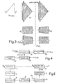
- FIG. 1 which represents a first embodiment of a correction system, applied to the correction of the residual transmodulation, a television signal at composite intermediate frequency, image and sound
- S F i is applied to the input a coupler 1 which takes part of this signal to transmit it to the input of a sound rejector filter 2 whose output delivers an intermediate frequency signal which now only contains the image components.
- the main output of the coupler 1 is connected to the signal input E i of a correction cell 3.
- This correction cell has a premodulation control input of amplitude C MA to which is applied a control signal obtained at from the image signal as follows:
- the output of the sound rejector filter 2 is connected to the input of an amplifier 4 whose output is connected to the input of a detection circuit 5.
- This detection circuit transmits at its output the detected video video signal.
- the output of this detection circuit is connected to an adjustable attenuator 6 which fixes the effectiveness of the correction by the level of the image video signal applied to the control input of the correction cell 3.
- the correction cell is such that its gain is only changed around a frequency called cell tuning frequency.
- FIG. 2 A detailed diagram of an embodiment of the correction cell 3 is shown in FIG. 2. A part of the essential elements of this cell are identical to those of the group delay correction cell described in the application for Patent N ° 74 35448 in the name of the applicant, for a differential phase correction device.
- the input E i of this cell is connected to output S by two parallel channels, a direct channel and a compensated channel.
- This cell differs from conventional group time correction cells by the fact that the transmittance of the modulation circuit of the compensated channel is constant at the tuning frequency, whatever the group delay time. Thus the correction of group delay time can be carried out independently without corresponding readjustment of the amplitude.
- the direct channel mainly comprises a resistor 10 and a capacitor 11 in series in the basic circuit of a NRN transistor 12 whose collector is connected to ground, and whose emitter is coupled to output 5 by a resistor 13. This direct channel therefore transmits without modifying all the components (image and sound) of the intermediate frequency composite signal applied to the input E 1 .
- the compensated channel includes an NPN amplifier transistor 14, the base of which is connected to the input E 1 , the emitter of which is coupled to ground by a resistance circuit 15 and potentiometer 16 enabling the resistance in the circuit to be adjusted. transmitter.
- This transistor constitutes a generator with constant impedance for the correction circuit and a separator with respect to the input impedance.
- the collector of transistor 14 is coupled to the group delay time modulation circuit 50, comprising a resistor 17 connected to a terminal of a tunable oscillating circuit with inductance coil 18 and capacitor 19.
- This modulation circuit further comprises an autotransformer 20, arranged between the collector of transistor 14 and ground, the midpoint of which is connected by a capacitor 21 and a PIN diode 22 to the terminal common to the oscillating circuit and to resistor 17.
- This same terminal is coupled to the output S of the correction cell by a resistor 23 in series with a capacitor 24, the emitter base junction of an NPN transistor 25 and a resistor 26, the collector of the transistor being connected to ground.
- An adjustable capacitor 27 in parallel on the resistor 26 makes it possible to adjust the phase between the direct channel and the compensated channel.
- Transistors 12 and 25 form a summator with high input impedance.
- the current in the PIN diode 22 is modulated by a control input E 2 connected by a resistor 28 to the cathode of this diode, the resistance of this PIN diode, variable with this current, causing a modification of the overvoltage coefficient therefore of the slope of the phase-frequency characteristic at the tuning frequency, this slope being the group delay time, the gain of this cell being unchanged.
- the gain of this cell can be kept constant as part of a differential phase correction, it can also be made variable without affecting the phase.
- a premodulation of amplitude as a function of the disturbing signal is applied, at the frequency selected by the oscillating circuit, by variation of the current in the emitter of the transistor 14.
- the correction cell further comprises, between the input of amplitude premodulation control C MA and the emitter of transistor 14, an amplitude premodulation control circuit 100 comprising a resistor 101 and a capacitor 102, the point common to these two elements being connected to the anode d a PIN 103 diode, the cathode of which is connected to ground.
- the gain of the group delay time correction cell is increased, at the tuning frequency of this cell, in a ratio defined by adjusting the correction efficiency by the adjustable attenuator 6, FIG. 1.
- the group delay time correction cell tuned to the frequency of the sound carrier at intermediate frequency by the oscillating circuit, realizes an amplitude expansion of this carrier sound frequency modulated, function of the video signal applied to the control input C MA , the transmodulation fault introduced by the power stage being a compression of the sound as a function of the video signal.
- FIG. 3 represents a signal diagram making it possible to illustrate the inter-modulation distortion and the correction of this distortion by selective premodulation at the frequency of the sound carrier.
- the second line of this diagram shows the sound carrier, before and after amplification, when there is no intermodulation correction.
- the sound carrier P s is amplitude modulated by the image signal and gives a distorted sound carrier (P s ) d by compression proportional to the amplitude of the video image frequency signal.
- the cell pre-modulates the sound carrier by expansion proportional to the amplitude of the video frequency signal (P ⁇ ) fM , the pre-modulated sound carrier, so that, after amplification, the sound carrier is corrected intermodulation (Ps) c; (P ⁇ ) ⁇ M and (Ps) c have been represented on the last line of the diagram.
- a similar cell comprising the same control circuit, but tuned to the image carrier frequency allows the correction of the amplitude distortions of this carrier not corrected by other correction devices, and, for example the correction of the compression of the pulses.
- the signal applied to the control input C MA of the cell tuned to the image carrier consists of synchronization pulses, the detection circuit 5 being provided with a Vs (dotted line in FIG. 1) making it possible to fix a threshold beyond which the detected signal is transmitted. The gain of the cell is then increased only for the synchronization pulses, the threshold voltage V s being fixed so that these pulses are only transmitted by the detection circuit.
- a similar cell tuned to the frequency of the chrominance subcarrier makes it possible to carry out a differential gain pre-correction whose shape is defined by the video frequency modulation signal applied to the modulation control input C MA .
- FIG. 4 shows a second embodiment of the correction system according to the invention applied to the incident phase correction.
- This correction is applied to the image carrier originating from the local oscillator at intermediate frequency in order to compensate for the phase shifts of this carrier, due to the video-modulation signal, by a premodulation of the phase of this carrier.
- the modulator 30 receives the video signal, Svideo, and this pre-modulated carrier in phase (P ! ) ? M from a correction cell 31 which receives on its signal input the intermediate frequency carrier FI of a local oscillator. 32 and a phase C MP pre-modulation control signal derived from the video signal after attenuation.
- the intermediate frequency modulated signal available at the output of the modulator is then amplified in the intermediate frequency amplifier 33 which supplies the signal S FI .
- the control signal C MP can be directly derived from the input video signal Svideo for pre-correction or be derived from the video signal detected after amplification by the power stage for an automatic correction system.
- the correction cell used in this system is the cell described above with reference to FIG. 2 without the amplitude premodulation control circuit 100, but with a phase premodulation control circuit 200, also shown in the figure 2, which makes it possible to vary the tuning conditions of the oscillating circuit 18, 19.
- This circuit includes varactor diodes, head to tail 201 and 202, in parallel on the oscillating circuit whose cathodes are connected to control C MA to vary the capacity and therefore the tuning frequency of the oscillating circuit.
- the gain of the cell is not modified but the shift of the characteristic on the frequency axis leads to a phase modulation which compensates for the incidental phase.
- a correction system using several cells tuned to frequencies of different carriers makes it possible to act independently on the group delay time, the amplitude, and the phase of each of these carriers and of implement for each of them and for each of these parameters a control of the correction tion.
- the transmission and retransmission equipment implements several group delay time correction cells, the poles of which are distributed in the frequency band, in order to linearize the phase and to make the group delay time constant in the entire transmission band.
- the control signal applied to the amplification premodulation input of the correction cell tuned to the frequency of the sound carrier is an error signal characteristic of the difference between the detected mean value and the value nominal average of this carrier.
- the correction system shown in FIG. 5 comprises, connected to the intermediate frequency input S FI, a coupler 1, the main output of which is connected to the input E i of the correction cell 3, and the other of which output is connected to the input of a bandpass filter 7 filtering the sound carrier, the output of this filter being connected to the input of amplifier 4; the output of this amplifier is connected to a mean value detector circuit 8, the output of which is connected to the first input of a comparator 9, the second input of this comparator receiving a reference signal V R , characteristic of the mean value nominal of the sound carrier.
- the output of this comparator 9 is connected to the adjustable attenuator 6 which supplies the amplitude modulation control signal C MA to the correction cell.
- the regulation of the mean value of the sound carrier makes it possible to maintain the image-sound ratio at the nominal value provided during transmission, this being particularly useful in re-transmitters when this ratio has been modified due to the propagation conditions between the transmitter and the retransmitter.
Landscapes
- Engineering & Computer Science (AREA)
- Multimedia (AREA)
- Signal Processing (AREA)
- Amplitude Modulation (AREA)
- Television Receiver Circuits (AREA)
- Picture Signal Circuits (AREA)
- Color Television Systems (AREA)
- Processing Of Color Television Signals (AREA)
- Cable Transmission Systems, Equalization Of Radio And Reduction Of Echo (AREA)
- Networks Using Active Elements (AREA)
Priority Applications (1)
| Application Number | Priority Date | Filing Date | Title |
|---|---|---|---|
| AT83400121T ATE16877T1 (de) | 1982-01-28 | 1983-01-19 | Anordnung zur korrektur der nichtlinearitaet durch zwischenfrequenz-vormodulation in einer fernseheinrichtung. |
Applications Claiming Priority (2)
| Application Number | Priority Date | Filing Date | Title |
|---|---|---|---|
| FR8201354A FR2520572B1 (fr) | 1982-01-28 | 1982-01-28 | Systeme de correction de non-linearites par premodulation en frequences intermediaires dans un equipement de television |
| FR8201354 | 1982-01-28 |
Publications (2)
| Publication Number | Publication Date |
|---|---|
| EP0086124A1 EP0086124A1 (fr) | 1983-08-17 |
| EP0086124B1 true EP0086124B1 (fr) | 1985-12-04 |
Family
ID=9270419
Family Applications (1)
| Application Number | Title | Priority Date | Filing Date |
|---|---|---|---|
| EP83400121A Expired EP0086124B1 (fr) | 1982-01-28 | 1983-01-19 | Système de correction de non linéarités par prémodulation en fréquences intermédiaires dans un équipement de télévision |
Country Status (10)
| Country | Link |
|---|---|
| US (1) | US4538180A (enExample) |
| EP (1) | EP0086124B1 (enExample) |
| JP (1) | JPS58133052A (enExample) |
| AR (1) | AR230544A1 (enExample) |
| AT (1) | ATE16877T1 (enExample) |
| CA (1) | CA1202412A (enExample) |
| DE (1) | DE3361362D1 (enExample) |
| FR (1) | FR2520572B1 (enExample) |
| GR (1) | GR77896B (enExample) |
| MX (1) | MX153233A (enExample) |
Families Citing this family (5)
| Publication number | Priority date | Publication date | Assignee | Title |
|---|---|---|---|---|
| GB2164823A (en) * | 1984-09-17 | 1986-03-26 | Philips Electronic Associated | Television transmitter |
| US5093725A (en) * | 1990-06-22 | 1992-03-03 | At&T Bell Laboratories | Dynamic signal modification for achieving interference reduction in concurrently transmitted signals |
| US5432562A (en) * | 1993-01-26 | 1995-07-11 | U.S. Philips Corporation | Television signal reception |
| US5430498A (en) * | 1994-03-01 | 1995-07-04 | Comark Communications, Inc. | Selective intermodulation correction system |
| FI104450B (fi) * | 1997-10-09 | 2000-01-31 | Nokia Networks Oy | Menetelmä ja kytkentä viiveen kompensoimiseksi tehovahvistimen linearisointisilmukassa |
Family Cites Families (4)
| Publication number | Priority date | Publication date | Assignee | Title |
|---|---|---|---|---|
| NL6909969A (enExample) * | 1968-07-02 | 1970-01-06 | ||
| FR2299759A1 (fr) * | 1974-10-22 | 1976-08-27 | Lgt Lab Gen Telecomm | Dispositif correcteur de phase differentielle et emetteur de television comportant un tel dispositif |
| US4249214A (en) * | 1979-03-23 | 1981-02-03 | Rca Corporation | Exciter having incidental phase correction compensation in consonance with output power level |
| FR2482799A1 (fr) * | 1980-05-14 | 1981-11-20 | Lgt Lab Gen Telecomm | Dispositif de precorrection de produits de non linearite et systeme de transmission de signaux de television comportant de tel dispositif |
-
1982
- 1982-01-28 FR FR8201354A patent/FR2520572B1/fr not_active Expired
-
1983
- 1983-01-13 US US06/457,624 patent/US4538180A/en not_active Expired - Fee Related
- 1983-01-19 AT AT83400121T patent/ATE16877T1/de not_active IP Right Cessation
- 1983-01-19 EP EP83400121A patent/EP0086124B1/fr not_active Expired
- 1983-01-19 DE DE8383400121T patent/DE3361362D1/de not_active Expired
- 1983-01-20 MX MX195974A patent/MX153233A/es unknown
- 1983-01-25 CA CA000420177A patent/CA1202412A/en not_active Expired
- 1983-01-26 JP JP58011200A patent/JPS58133052A/ja active Pending
- 1983-01-26 GR GR70341A patent/GR77896B/el unknown
- 1983-01-27 AR AR291956A patent/AR230544A1/es active
Non-Patent Citations (1)
| Title |
|---|
| ELECTRICAL COMMUNICATION, vol. 48, no. 4, 1973, Londres, GB, J. IRMER et al.: "20 KW UHF Television transmitter with all solid state driver for klystron amplifiers" * |
Also Published As
| Publication number | Publication date |
|---|---|
| AR230544A1 (es) | 1984-04-30 |
| FR2520572B1 (fr) | 1986-01-17 |
| DE3361362D1 (en) | 1986-01-16 |
| CA1202412A (en) | 1986-03-25 |
| JPS58133052A (ja) | 1983-08-08 |
| US4538180A (en) | 1985-08-27 |
| EP0086124A1 (fr) | 1983-08-17 |
| ATE16877T1 (de) | 1985-12-15 |
| GR77896B (enExample) | 1984-09-25 |
| MX153233A (es) | 1986-08-28 |
| FR2520572A1 (fr) | 1983-07-29 |
Similar Documents
| Publication | Publication Date | Title |
|---|---|---|
| EP0040127B1 (fr) | Dispositif de transmission de signaux comportant un circuit de précorrection de produits de non linéarité | |
| US5678198A (en) | System for controlling signal level at both ends of a transmission link, based upon a detected value | |
| US5680238A (en) | Hybrid SCM optical transmission apparatus | |
| FR2670631A1 (fr) | Agencement d'amplificateurs montes en parallele avec moyen de controle des phases et procede d'amplification correspondant. | |
| EP0086124B1 (fr) | Système de correction de non linéarités par prémodulation en fréquences intermédiaires dans un équipement de télévision | |
| EP0169093B1 (fr) | Récepteur á démodulateur de fréquence pour système de télévision à multiplexage temporal | |
| EP0010023B1 (fr) | Système de transmission en modulation d'amplitude à haute performance et émetteur et réémetteur de télévision comportant un tel système | |
| FR2471718A1 (fr) | Systeme de copie d'un signal video couleur | |
| EP0141715B1 (fr) | Dispositif de précorrection automatique des non-linéarités dans une chaîne d'amplification de puissance, et son application à un émetteur de télévision | |
| EP0081413B1 (fr) | Equipement de retransmission de signal de télévision en voie commune, à commande automatique du rapport image-son | |
| US6671465B1 (en) | Apparatus and methods for improving linearity and noise performance of an optical source | |
| EP0064431B1 (fr) | Dispositif de correction de non-linéarité vidéofréquence à efficacité sélective | |
| EP0887953A2 (en) | Apparatus and methods for improving linearity and noise performance of an optical source | |
| EP0028181B1 (fr) | Dispositif de précorrection en haute fréquence de la non linéarité des amplificateurs de signaux comportant au moins un signal porteur modulé en amplitude, et émetteur de télévision comportant un tel dispositif | |
| EP1315295B1 (fr) | Tuner comprenant un filtre sélectif | |
| FR2509104A1 (fr) | Televiseur multistandards pour la reception d'emissions dont l'onde porteuse " son " est modulee, soit en frequence, soit en amplitude | |
| EP0117960B1 (fr) | Circuit et procédé de réglage automatique de la fréquence centrale d'un filtre | |
| EP0149950A2 (fr) | Emetteur de télévision comportant un klystron commun pour l'image et le son | |
| JP3714646B2 (ja) | 副搬送波変調光送信器および副搬送波変調光受信器 | |
| CH406296A (fr) | Installation de transmission d'un signal au moyen d'une onde modulée en fréquence | |
| FR2507417A1 (fr) | Systeme de restitution de signaux video | |
| JP2011120035A (ja) | 映像信号受信装置及び映像伝送システム | |
| WO1994024760A1 (fr) | Dispositif d'amplification de signaux de television a classe de fonctionnement variable, predeterminee pour l'elimination des erreurs de transmission | |
| BE480313A (enExample) | ||
| CH264772A (fr) | Dispositif pour l'élimination d'interférences dans une installation d'émission d'ondes. |
Legal Events
| Date | Code | Title | Description |
|---|---|---|---|
| PUAI | Public reference made under article 153(3) epc to a published international application that has entered the european phase |
Free format text: ORIGINAL CODE: 0009012 |
|
| AK | Designated contracting states |
Designated state(s): AT CH DE GB IT LI SE |
|
| 17P | Request for examination filed |
Effective date: 19840118 |
|
| ITF | It: translation for a ep patent filed | ||
| GRAA | (expected) grant |
Free format text: ORIGINAL CODE: 0009210 |
|
| RAP1 | Party data changed (applicant data changed or rights of an application transferred) |
Owner name: THOMSON-LGT LABORATOIRE GENERAL DES TELECOMMUNICAT |
|
| AK | Designated contracting states |
Designated state(s): AT CH DE GB IT LI SE |
|
| REF | Corresponds to: |
Ref document number: 16877 Country of ref document: AT Date of ref document: 19851215 Kind code of ref document: T |
|
| REF | Corresponds to: |
Ref document number: 3361362 Country of ref document: DE Date of ref document: 19860116 |
|
| PLBE | No opposition filed within time limit |
Free format text: ORIGINAL CODE: 0009261 |
|
| STAA | Information on the status of an ep patent application or granted ep patent |
Free format text: STATUS: NO OPPOSITION FILED WITHIN TIME LIMIT |
|
| 26N | No opposition filed | ||
| PGFP | Annual fee paid to national office [announced via postgrant information from national office to epo] |
Ref country code: AT Payment date: 19870130 Year of fee payment: 5 |
|
| PG25 | Lapsed in a contracting state [announced via postgrant information from national office to epo] |
Ref country code: AT Effective date: 19890119 |
|
| PG25 | Lapsed in a contracting state [announced via postgrant information from national office to epo] |
Ref country code: SE Effective date: 19890120 |
|
| PG25 | Lapsed in a contracting state [announced via postgrant information from national office to epo] |
Ref country code: LI Effective date: 19890131 Ref country code: CH Effective date: 19890131 |
|
| REG | Reference to a national code |
Ref country code: CH Ref legal event code: PL |
|
| PGFP | Annual fee paid to national office [announced via postgrant information from national office to epo] |
Ref country code: DE Payment date: 19891223 Year of fee payment: 8 |
|
| PGFP | Annual fee paid to national office [announced via postgrant information from national office to epo] |
Ref country code: GB Payment date: 19891231 Year of fee payment: 8 |
|
| ITTA | It: last paid annual fee | ||
| PG25 | Lapsed in a contracting state [announced via postgrant information from national office to epo] |
Ref country code: GB Effective date: 19910119 |
|
| GBPC | Gb: european patent ceased through non-payment of renewal fee | ||
| PG25 | Lapsed in a contracting state [announced via postgrant information from national office to epo] |
Ref country code: DE Effective date: 19911001 |
|
| EUG | Se: european patent has lapsed |
Ref document number: 83400121.6 Effective date: 19891205 |