EP0084844B1 - Fet circuits - Google Patents
Fet circuits Download PDFInfo
- Publication number
- EP0084844B1 EP0084844B1 EP83100399A EP83100399A EP0084844B1 EP 0084844 B1 EP0084844 B1 EP 0084844B1 EP 83100399 A EP83100399 A EP 83100399A EP 83100399 A EP83100399 A EP 83100399A EP 0084844 B1 EP0084844 B1 EP 0084844B1
- Authority
- EP
- European Patent Office
- Prior art keywords
- fet
- circuit
- input terminal
- terminal
- accordance
- Prior art date
- Legal status (The legal status is an assumption and is not a legal conclusion. Google has not performed a legal analysis and makes no representation as to the accuracy of the status listed.)
- Expired
Links
- 239000002131 composite material Substances 0.000 claims description 11
- 230000009977 dual effect Effects 0.000 claims description 5
- 238000010586 diagram Methods 0.000 description 13
- 230000003068 static effect Effects 0.000 description 6
- 230000007423 decrease Effects 0.000 description 5
- 230000003247 decreasing effect Effects 0.000 description 5
- 238000004519 manufacturing process Methods 0.000 description 3
- 230000004048 modification Effects 0.000 description 3
- 238000012986 modification Methods 0.000 description 3
- 229910001218 Gallium arsenide Inorganic materials 0.000 description 2
- 230000009471 action Effects 0.000 description 1
- 230000004888 barrier function Effects 0.000 description 1
- 230000008901 benefit Effects 0.000 description 1
- 230000008859 change Effects 0.000 description 1
- 230000001419 dependent effect Effects 0.000 description 1
- 230000005669 field effect Effects 0.000 description 1
- 238000003780 insertion Methods 0.000 description 1
- 230000037431 insertion Effects 0.000 description 1
- 230000010354 integration Effects 0.000 description 1
- 239000002184 metal Substances 0.000 description 1
- 230000004044 response Effects 0.000 description 1
- 230000000717 retained effect Effects 0.000 description 1
- 239000004065 semiconductor Substances 0.000 description 1
- 238000004088 simulation Methods 0.000 description 1
- 230000006641 stabilisation Effects 0.000 description 1
- 238000011105 stabilization Methods 0.000 description 1
- 239000000758 substrate Substances 0.000 description 1
- 230000001360 synchronised effect Effects 0.000 description 1
Images





Classifications
-
- H—ELECTRICITY
- H03—ELECTRONIC CIRCUITRY
- H03K—PULSE TECHNIQUE
- H03K3/00—Circuits for generating electric pulses; Monostable, bistable or multistable circuits
- H03K3/02—Generators characterised by the type of circuit or by the means used for producing pulses
- H03K3/353—Generators characterised by the type of circuit or by the means used for producing pulses by the use, as active elements, of field-effect transistors with internal or external positive feedback
- H03K3/356—Bistable circuits
- H03K3/356017—Bistable circuits using additional transistors in the input circuit
- H03K3/356034—Bistable circuits using additional transistors in the input circuit the input circuit having a differential configuration
-
- H—ELECTRICITY
- H03—ELECTRONIC CIRCUITRY
- H03K—PULSE TECHNIQUE
- H03K3/00—Circuits for generating electric pulses; Monostable, bistable or multistable circuits
- H03K3/02—Generators characterised by the type of circuit or by the means used for producing pulses
- H03K3/353—Generators characterised by the type of circuit or by the means used for producing pulses by the use, as active elements, of field-effect transistors with internal or external positive feedback
- H03K3/356—Bistable circuits
- H03K3/356017—Bistable circuits using additional transistors in the input circuit
- H03K3/356034—Bistable circuits using additional transistors in the input circuit the input circuit having a differential configuration
- H03K3/356043—Bistable circuits using additional transistors in the input circuit the input circuit having a differential configuration with synchronous operation
-
- H—ELECTRICITY
- H03—ELECTRONIC CIRCUITRY
- H03K—PULSE TECHNIQUE
- H03K3/00—Circuits for generating electric pulses; Monostable, bistable or multistable circuits
- H03K3/02—Generators characterised by the type of circuit or by the means used for producing pulses
- H03K3/353—Generators characterised by the type of circuit or by the means used for producing pulses by the use, as active elements, of field-effect transistors with internal or external positive feedback
- H03K3/356—Bistable circuits
- H03K3/356017—Bistable circuits using additional transistors in the input circuit
- H03K3/356052—Bistable circuits using additional transistors in the input circuit using pass gates
- H03K3/35606—Bistable circuits using additional transistors in the input circuit using pass gates with synchronous operation
-
- H—ELECTRICITY
- H03—ELECTRONIC CIRCUITRY
- H03K—PULSE TECHNIQUE
- H03K3/00—Circuits for generating electric pulses; Monostable, bistable or multistable circuits
- H03K3/02—Generators characterised by the type of circuit or by the means used for producing pulses
- H03K3/353—Generators characterised by the type of circuit or by the means used for producing pulses by the use, as active elements, of field-effect transistors with internal or external positive feedback
- H03K3/356—Bistable circuits
- H03K3/356069—Bistable circuits using additional transistors in the feedback circuit
Definitions
- the present invention relates to a FET circuit according to the prior art portion of claim 1.
- the invention is especially applicable to circuits of metal semiconductor field effect transistors (herein after referred to a MESFET) which constitute a latch circuit.
- a MESFET metal semiconductor field effect transistors
- Such a FET circuit is disclosed e.g. in the publication "Threshold voltage margin of normally off GaAs MESFET in DCFL Circuit", Ino et al., IEEE Electron Device letters, Vol. EDL 2, No. 6, p. 144-145, 1981.
- Fig. 1 shows a conventional latch comprising normally-offtype MESFETs wherein the threshold voltage V T of the MESFETs is positive.
- the conventional latch circuit has a pair of MESFETs Q 11 and Q 12 which are connected by their sources to a common grounding terminal 12, by their drains through respective resistors R 11 and R 12 to a positive power supply terminal 11, and by their gate electrodes to the drain electrode of the other MESFET Q 12 or Q 11 , respectively.
- the output terminals 13 and 14 are connected to the drains of the MESFETs Q 11 and Q 12 , respectively.
- the voltage V L is gate input voltage of the MESFET Q 12 , and in order to change the MESFET Q 12 to off state the below mentioned relation is necessary:
- an "H" level voltage V H at the output terminal 14 is V DD at this time, or becomes V DI , for a case where the power supply voltage V DD is higher than Schottky barrier voltage V DI ; ad in order to make the MESFET Q 11 on by the V H voltage at the output terminal 14 the next relation is necessary:
- Fig. 3 shows another conventional example of latch using normally-on type MESFETs having negative threshold voltage in this Fig. 3.
- MESFETS Q 3 , and Q 32 correspond to MESFETs Q 11 and Q 12 of Fig. 1 and resistors R 31 and R 32 correspond to resistors R 11 and R 12 of Fig. 1, respectively.
- this circuit of Fig. 3 there are two additional MESFETs Q 33 and Q 34 which are connected by their gates to the drains of the MESFETs Q 31 and Q 32 , respectively, and by their sources through diodes D 3 ,, D 32 and D 33 to the output terminal 33 and D 34 , D 35 and D 36 to the output terminal 34, respectively, and by their drains commonly to a power supply terminal 31.
- This circuit has two negative power supply terminals, namely a first negative power supply terminal 32 corresponding to 12 of Fig. 1 and another negative power supply terminal 35 to which load resistors R 33 and R 34 of the source- follower MESFETs Q 33 and Q 34 are commonly connected.
- the diodes D 31 to D 33 and D 34 to D 36 are for leveling down source follower outputs so as to meet the input levels.
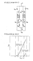
- normally-on type MESFET has an advantage of providing a larger on-current than normally-off type MESFET as shown in Fig. 4 and in the circuit of Fig. 3. By this large on-current, logic swing of the circuit is expanded thereby resulting in increasing of allowable range of deviation of the threshold voltage ⁇ V T to be 0.5 to 1.0 V.
- FET latch circuits comprising a pair of crosscoupled inverters, each inverter comprising a resistive load and an input-stage FET, the sources of the input stage FETs being connected to a common-connection point, are disclosed in the publication "IBM Technical Disclosure Bulletin” Vol. 14, No. 1, June 1971, page 208, and in the publication "Electronics", Vol. 52, No. 9, April 1979, pages 125 to 135.
- a FET composite circuit with a R-S type flip-flop having output terminals, set and reset terminals, a clock input terminal and a reference input terminal is disclosed in GB-A-2,081,041. From the publication "Orient l'Electronique” No. 354, April 1971, pages 27 to 32, it is known to connect two R-S flip-flops together to form a master slave delay flip-flop. This master slave delay flip-flop has no reference inputs and, therefore, the reference input of one flip-flop is not connected to the clock input of the other flip-flop.
- Fig. 5 shows a first example of a latch embodying the present invention.
- the latch comprises a pair of inverters Q 51 +Q 53 and Q 52 +Q 54 .
- Each of the inverters comprises input stage FET Q 51 or Q 52 and a source follower FET Q 53 or Q 54 .
- Each input stage FET is connected by its gate electrode to the source of the source follower FET Q 14 or Q 53 of the other inverter through a diode D 52 or D 51'
- Each source follower FET Q S4 , Q 53 is connected by its gate to the drain of the input stage FET Q 52 or Q 51 and through a resistor R 52 or R 51 to a positive side power supply terminal 51.
- the sources of the input stage FET Q 51 and Q 52 are connected in common to a common connected point C and further a resistor R 55 as current source means is connected between common connected point C and the negative side power supply or ground terminal 52.
- Output terminals 53 and 54 are connected to junction points between the diode 51 and the gate electode of the FET Q 52 or to the junction point between the diode D 52 and the gate electrode of the FET 51, respectively, and the gate electrodes of the FET Q 51 and Q 52 are connected to the negative power supply terminal 52 through a resistor R 53 and R 54 , respectively.
- the resistors R 5 , and R 52 are load resistors of the MESFETs Q 51 and Q S2 , respectively, and resistors R 53 and R 54 are load resistors of the source follower MESFETs Q 54 and Q 53 , respectively.
- the diodes D 51 and D 52 are for adjusting the input levels to the MESFETs Q 52 and Q 51 , respectively.
- the output terminal 53 and 54 are of positive phase output and negative phase output, respectively.
- threshold voltage of the MESFETs decrease, then on-current ION of the MESFET Q 51 increases, and the "L" level voltage V L decreases. Accordingly, when the resistor R 55 is large, then the above-mentioned inequality (6) holds for a wide range of the threshold voltage V T , and the latch performs a stable operation.
- Fig. 6 is a graph showing allowable range of the threshold voltage V T of the MESFETs for performing normal performance as latch, simulated by computer.
- the latch performs stable operation for a wide range of the threshold voltage V T between -0.6V and 0.3V.
- the critical voltage V c is always between the levels of "H” and "L”, and accord-' ingly the latch is very superior with respect to noise margin. Therefore in this circuit the deviations of the threshold voltage ⁇ V T of the MESFETs are allowed to 0.9V, therefore difficulties of controlling of the threshold voltage in manufacturing process of the MESFETs is greatly eased.
- Fig. 7 shows a circuit diagram of a second example embodying the present invention.
- this example in order to increase allowable threshold voltage ranges of the MESFETs plural stages of level shifting diodes D 51 , D 53 and D 55 and D 52 , D 54 and D 56 are used, and in order to increase logic swing of the MESFETs Q 51 and Q 52 by increasing the on-currents by selecting the threshold voltage V T of the MESFETs Q 51 and Q 52 deeper, a second negative power supply terminal 55 is provided and a pair of resistors R 53 and R 54 are connected respectively from the gate electrodes of the MESFET Q 51 and Q 52 to the common second negative power supply terminal 55.
- the level shifting diodes D 51 to D 56 should be selected to a desired number in order to meet desired input- output levels.
- the diode D 57 and D 58 which are connected between respective resistors R 51 and R 52 and the positive power supply terminal 51, are for increasing operation characteristic of the MESFETs Q 53 and Q 54 so as to operate in the current saturation region thereby increasing response of the source followers, and their number may be changed responding to the thereshold voltages of the MESFETs.
- Fig. 8 shows a circuit diagram of a third example which is a clocked reset-set flip-flop using the latch of Fig. 5.
- a MESFET Q 56 is connected by its drain to the common-connection point C, and by its gate to the reference input terminal 56.
- Another MESFET Q 55 is connected by its gate to a clock input terminal 55 and by its source commonly with the source of the MESFET Q 56 to the upper end of the current source means R 55 .
- MESFETS Q 57 and Q 58 are common-connected with their sources to the drain of the MESFET Q 55 .
- the gate of the MESFET Q s7 is connected to a reset input terminal 57.
- the gate of the MESFET Q 58 is connnected to a set input terminal 58, drains of the MESFETs Q s7 and Q 58 are connected to the drains of MESFET Q 51 and Q 52 , respectively.
- the output terminals 53 and 54 are led out to a positive phase Q terminal 53 and negative phase Q terminal 54, respectively.
- the resistors R 51 and R s2 serve as common- resistors for common drain connected MESFETs Q 51 , Q 57 and the common drain connected MESFETs Q 52 , Q 58 , respectively.
- MESFETs Q 51' Q 52 , Q 53 and Q 54 form a latch circuit, and therefore above-mentioned state which is designated by the state at the reset input terminal 57 and set input terminal 58 is retained as it is. And then this state is output from the output terminals 53 and 54.
- This clocked reset-set flip-flop has such small power consumption as is substantially equal to that of the latch of Fig. 5, and allowable margin to the deviation of the threshold voltage of the latch is reflected to this flip-flop. That is, in the operation of increasing or decreasing the on-current due to deviation of the threshold voltage the voltage of the common-connected sources of the MESFETs Q 55 and Q 56 increases or decreases, but the allowable range of the threshold voltage of this flip-flop are equal to those of the latch since the potential of the reference input terminal 56 can be selected so as to certainly turn on or off the MESFETs Q 55 and Q 56'
- the clocked reset-set flip-flop using the MESFET circuit in accordance with the present invention is operable at a very low power consumption and can stably operate for a wide range of threshold voltage.
- Fig. 9 is a circuit diagram of a master-slave delay flip-flop of single phase clocked type which comprises the reset-set flip-flop shown in Fig. 8.
- the reset-setflip-flops 91 and 92 are a master flip-flop and a slave flip-flop, respectively.
- the set input terminal S, reset input terminal R, clock input terminal C, reference voltage input terminal REF, positive phase output terminal Q and negative phase output terminal Q correspond to the terminals 58, 57, 55, 56, 53 and 54, respectively.
- the first stage reset-set flip-flop 91 and the second stage reset-set flip-flop 92 are connected such that output terminals Q and Q of the former 91 are connected to the input terminals S and R of the latter 92, respectively, a clock input terminal C of the former 91 and a reference input terminal REF of the latter 92 are connected in common to a clock- input terminal 93 of the composite circuit, a reference input terminal REF of the former 91 and a clock input terminal C of the latter 92 are connected in common to a first reference input terminal 94 of the composite circuit, a reset input terminal R of the former 91 is connected to a second reference input terminal 96, and a set input terminal S of the former 91 is connected to a set input terminal 95 of the composite circuit, and output terminals Q and Q of the latter 92 are connected to the output terminals 97 and 98 of the composite circuit, respectively.
- the input gates S and R opens and signals at the set input terminal is compared with the signal at the second reference voltage input terminal 96, and issues positive phase output and negative phase output from the output terminals Q and Q of the master flip-flop 91, respectively.
- the input gate S and R are shut off.
- each of the flip-flop 91 and 92 a pair of the clock input terminal C and the reference voltage input terminal REF as well as the pair of set input terminal S and the reset input terminal R forms each-other differential input relation, and in each pair both inputs are compared to determine the input logic. Accordingly, by fixing one signal of the pair in DC voltage relation, it is possible to operate the circuit with only single phase signal. As a result for the clock input, only a single phase clock suffices. And furthermore there is no need of adding inverter to the input terminals S and R of the master flip-flop 91, and only simply impressing an input signal to input terminals suffices.
- a clocked master-slave delay flip-flop can be constituted only with two reset-set flip-flop and without using inverter, thereby decreasing of area of IC chip and power consumption is possible. Furthermore by using only a single phase clock signal the master-slave flip-flop can be synchronized without delay and accurate operation is possible even at a high speed operation.
- level shift diode D S1 and D 52 series connected multiple diodes may be used depending on the extent of the level to be shifted thereby operation for large pinch off voltage Vp of MESFET can be possible.
- the master-slave flip-flop of a single phase clocked type can be realized with dispensing with the inverter hitherto necessitated and thereby size of IC as well as power consumption can be decreased.
- Fig. 10- shows a static RAM constituted with the latch of Fig. 5.
- a pair of MESFETs Q 15 and G 16 are connected by their sources to the output terminals 53 and 54 of the latch of Fig. 5, respectively, and the gates of the MESFETs Q, 5 and Q 16 are commonly connected to a control terminal 15, and the drains of the MESFETS Q 15 and Q 16 are connected to write-in terminal 16 and 17, respectively.
- This static RAM has very small power consumption and can perform stable operation for wide range of threshold voltage of MESFETs, since the power consumption and allowable range of the threshold voltage is substantially the same as that of the latch of Fig. 5.
- circuit configurations of Fig. 5, Fig. 7, Fig. 8 and Fig. 10 are not limited to the circuits shown thereof, but instead, their current source means R 55 can be replaced by active load, for instance of drain-source impedance of a FET as shown in Fig. 11(a).
- active load for instance of drain-source impedance of a FET as shown in Fig. 11(a).
- Fig. 11(b) shows further improved example where as the current source means a dual gate FET connected with both of its gate to the source. Since the dual gate FET has more superior constant current characteristic than single gate FET, the circuit Fig. 11(b) wherein the dual gate FET Q 111' is connected with their dual gates to the source to serve as current source means R 55 can perform more superior characteristic than Fig. 11(a).
- the present invention is characterized by a latch circuit or its application with insertion of current source means between common-connection point C and the negative side power supply terminal 52.
Landscapes
- Logic Circuits (AREA)
Description
- The present invention relates to a FET circuit according to the prior art portion of
claim 1. - The invention is especially applicable to circuits of metal semiconductor field effect transistors (herein after referred to a MESFET) which constitute a latch circuit. Such a FET circuit is disclosed e.g. in the publication "Threshold voltage margin of normally off GaAs MESFET in DCFL Circuit", Ino et al., IEEE Electron Device letters, Vol. EDL 2, No. 6, p. 144-145, 1981.
- Fig. 1 shows a conventional latch comprising normally-offtype MESFETs wherein the threshold voltage VT of the MESFETs is positive. As shown in Fig. 1, the conventional latch circuit has a pair of MESFETs Q11 and Q12 which are connected by their sources to a
common grounding terminal 12, by their drains through respective resistors R11 and R12 to a positive power supply terminal 11, and by their gate electrodes to the drain electrode of the other MESFET Q12 or Q11, respectively. Theoutput terminals output terminals 
- At this time, the voltage VL is gate input voltage of the MESFET Q12, and in order to change the MESFET Q12 to off state the below mentioned relation is necessary:

- In the similar manner, an "H" level voltage VH at the
output terminal 14 is VDD at this time, or becomes VDI, for a case where the power supply voltage VDD is higher than Schottky barrier voltage VDI; ad in order to make the MESFET Q11 on by the VH voltage at theoutput terminal 14 the next relation is necessary:
- In this circuit if the threshold voltage VT decreases, the on current ION increases, and therefore the "L" level voltage VL decreases. However, since the threshold voltage VT has decreased, the above-mentioned relation of inequity (2) holds only for very limited range of the threshold voltage VT. When the threshold voltage VT increases, similarly the relation of the inequity (2) holds only for a small range of the threshold voltage VT.
- Detailed analysis of the above-mentioned relation has been made by circuit simulation by using computer and the simulated results are shown in a graph of FIG. 2, wherein curves VH and VL show "H" level voltage and "L" level voltage, respectively, and a line Vc shows voltages of
output terminals - From observation of the graph of Fig. 2 allowable range of the threshold voltage VT is about 0.1 to 0.2 volt. Accordingly, deviation ΔVT of the threshold voltage VT is allowed only a range ±50mV. And this ±50mV deviation corresponds to very accurate controlling of ±40A of 1000A thick channel layer when the MESFET is made with GaAs substrate and carrier concentration of a channel layer is 1017cm-3. And such very accurate controlling of the thickness is practically impossible when such logic circuits are manufactured with a high integration with a high manufacturing yield.
- Fig. 3 shows another conventional example of latch using normally-on type MESFETs having negative threshold voltage in this Fig. 3. MESFETS Q3, and Q32 correspond to MESFETs Q11 and Q12 of Fig. 1 and resistors R31 and R32 correspond to resistors R11 and R12 of Fig. 1, respectively. And in this circuit of Fig. 3 there are two additional MESFETs Q33 and Q34 which are connected by their gates to the drains of the MESFETs Q31 and Q32, respectively, and by their sources through diodes D3,, D32 and D33 to the
output terminal 33 and D34, D35 and D36 to theoutput terminal 34, respectively, and by their drains commonly to a power supply terminal 31. This circuit has two negative power supply terminals, namely a first negative power supply terminal 32 corresponding to 12 of Fig. 1 and another negativepower supply terminal 35 to which load resistors R33 and R34 of the source- follower MESFETs Q33 and Q34 are commonly connected. The diodes D31 to D33 and D34 to D36 are for leveling down source follower outputs so as to meet the input levels. Generally, normally-on type MESFET has an advantage of providing a larger on-current than normally-off type MESFET as shown in Fig. 4 and in the circuit of Fig. 3. By this large on-current, logic swing of the circuit is expanded thereby resulting in increasing of allowable range of deviation of the threshold voltage ΔVT to be 0.5 to 1.0 V. However this conventional latch of Fig. 3 has a shortcoming of a large operating current and necessity of many diodes for level adjustments of outputs and further necessitates two power supplies. Therefore its power consumption is very large such that 10 to 100 times power consumption than the conventional normally-off type MESFET latch. - FET latch circuits comprising a pair of crosscoupled inverters, each inverter comprising a resistive load and an input-stage FET, the sources of the input stage FETs being connected to a common-connection point, are disclosed in the publication "IBM Technical Disclosure Bulletin" Vol. 14, No. 1, June 1971, page 208, and in the publication "Electronics", Vol. 52, No. 9, April 1979, pages 125 to 135.
- A FET composite circuit with a R-S type flip-flop having output terminals, set and reset terminals, a clock input terminal and a reference input terminal is disclosed in GB-A-2,081,041. From the publication "Toute l'Electronique" No. 354, April 1971, pages 27 to 32, it is known to connect two R-S flip-flops together to form a master slave delay flip-flop. This master slave delay flip-flop has no reference inputs and, therefore, the reference input of one flip-flop is not connected to the clock input of the other flip-flop.
- In view of the above-mentioned disadvantages, it is an object of the invention to provide a FET latch circuit having an extended allowable range of threshold voltage of the transistor which is effective for a stable operation without increasing the power consumption.
- The solution of this object is especially defined in
claim 1. Advantageous embodiments are defined in dependent claims. - The invention will be explained in the following by means of the drawings in which:
- Fig. 1 is the circuit diagram of the conventional latch circuit using normally-off type MESFETs.
- Fig. 2 is the graph showing the relation between threshold voltage of the MESFETs and operation of the circuit of Fig. 1.
- Fig. 3 is the circuit diagram of the second conventional latch circuit using the normally-on type MESFETs..
- Fig. 4 is the graph showing the current-voltage characteristics of the normally on-type MESFETs and normally-off type MESFETs.
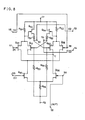
- Fig. 5 is a circuit diagram of a first embodiment of FET latch circuit embodying the present invention.
- Fig. 6 is a graph showing a relation between threshold voltage and operation characteristic of the latch circuit of Fig. 5.
- Fig. 7 is a circuit diagram of a second embodiment of FET latch circuit embodying the present invention.
- Fig. 8 is a circuit diagram of a clocked reset-set flip-flop embodying the present invention.
- Fig. 9 is a block diagram of a clocked master-slave delay flip-flop embodying the present invention.
- Fig. 10 is a circuit diagram of an example of a static RAM embodying the present invention.
- Fig. 11(a) is a circuit diagram of a part of modification of the examples of the present invention.
- Fig. 11(b) is a circuit diagram of a part of modification of the examples of the present invention.
- Fig. 12 is a circuit diagram of a part of modification of the examples of the present invention.
- The present invention is elucidated in detail referring to Fig. 5. and thereafter.
- Fig. 5 shows a first example of a latch embodying the present invention. As shown in Fig. 5 the latch comprises a pair of inverters Q51+Q53 and Q52+Q54. Each of the inverters comprises input stage FET Q51 or Q52 and a source follower FET Q53 or Q54.Each input stage FET is connected by its gate electrode to the source of the source follower FET Q14 or Q53 of the other inverter through a diode D52 or D51' Each source follower FET QS4, Q53 is connected by its gate to the drain of the input stage FET Q52 or Q51 and through a resistor R52 or R51 to a positive side
power supply terminal 51. The sources of the input stage FET Q51 and Q52 are connected in common to a common connected point C and further a resistor R55 as current source means is connected between common connected point C and the negative side power supply orground terminal 52.Output terminals diode 51 and the gate electode of the FET Q52 or to the junction point between the diode D52 and the gate electrode of theFET 51, respectively, and the gate electrodes of the FET Q51 and Q52 are connected to the negativepower supply terminal 52 through a resistor R53 and R54, respectively. The resistors R5, and R52are load resistors of the MESFETs Q51 and QS2, respectively, and resistors R53 and R54 are load resistors of the source follower MESFETs Q54 and Q53, respectively. The diodes D51 and D52 are for adjusting the input levels to the MESFETs Q52 and Q51, respectively. Theoutput terminal - . Operation of latch of Fig. 5 is as follows.
- When a MESFET Q51 is on and MESFET Q52 is off, then "L" level voltage VL is as follows:

- Ion is an on-current flowing through the resistor R51,
- VGS is gate-source voltage of the MESFET Q53.
- VD is voltage drop across the diode D51.
- At the same time "H" level voltage VH is as follows:

- Herein in order that the latch operates stably, to cut off the MESFET Q52 by the "L" level voltage VL the following relation is necessary:

- Now provided that threshold voltage of the MESFETs decrease, then on-current ION of the MESFET Q51 increases, and the "L" level voltage VL decreases. Accordingly, when the resistor R55 is large, then the above-mentioned inequality (6) holds for a wide range of the threshold voltage VT, and the latch performs a stable operation.
- Experimental and computor simulated study shows that D.C. resistance of the current source means R55 should be selected 5-50 times of each source-drain resistance of the on-MESFET Q51 and Q52, in order to perform good characteristics.
- Fig. 6 is a graph showing allowable range of the threshold voltage VT of the MESFETs for performing normal performance as latch, simulated by computer. As shown by the curves the latch performs stable operation for a wide range of the threshold voltage VT between -0.6V and 0.3V. And furthermore when the resistor R55 is sufficiently large, the critical voltage Vc is always between the levels of "H" and "L", and accord-' ingly the latch is very superior with respect to noise margin. Therefore in this circuit the deviations of the threshold voltage ΔVT of the MESFETs are allowed to 0.9V, therefore difficulties of controlling of the threshold voltage in manufacturing process of the MESFETs is greatly eased. Furthermore with respect to the power consumption of the latch, very little power consumption, 1/2 to 1/10 times of the conventional latch using the normally-on type MESFETs suffices to operate the latch in accordance with the present invention, since the threshold voltage is around 0V hand hence on-current is very small, only one pair of level shifting diodes D51 and D52 of one stage suffices, and a negative power supply is unnecessary.
- Fig. 7 shows a circuit diagram of a second example embodying the present invention. In this example in order to increase allowable threshold voltage ranges of the MESFETs plural stages of level shifting diodes D51, D53 and D55 and D52, D54 and D56 are used, and in order to increase logic swing of the MESFETs Q51 and Q52 by increasing the on-currents by selecting the threshold voltage VT of the MESFETs Q51 and Q52 deeper, a second negative
power supply terminal 55 is provided and a pair of resistors R53 and R54 are connected respectively from the gate electrodes of the MESFET Q51 and Q52 to the common second negativepower supply terminal 55. The level shifting diodes D51 to D56 should be selected to a desired number in order to meet desired input- output levels. The diode D57 and D58, which are connected between respective resistors R51 and R52 and the positivepower supply terminal 51, are for increasing operation characteristic of the MESFETs Q53 and Q54 so as to operate in the current saturation region thereby increasing response of the source followers, and their number may be changed responding to the thereshold voltages of the MESFETs. - Other parts and components of the circuit which are corresponding to the circuit of Fig. 5 are designated by the same numerals as them, and the elucidations on them are omitted for simplicity of the explanation.
- Fig. 8 shows a circuit diagram of a third example which is a clocked reset-set flip-flop using the latch of Fig. 5. In the circuit of Fig. 8 a MESFET Q56 is connected by its drain to the common-connection point C, and by its gate to the
reference input terminal 56. Another MESFET Q55 is connected by its gate to aclock input terminal 55 and by its source commonly with the source of the MESFET Q56 to the upper end of the current source means R55. MESFETS Q57 and Q58 are common-connected with their sources to the drain of the MESFET Q55. The gate of the MESFET Qs7 is connected to areset input terminal 57. The gate of the MESFET Q58 is connnected to a setinput terminal 58, drains of the MESFETs Qs7 and Q58 are connected to the drains of MESFET Q51 and Q52, respectively. Theoutput terminals phase Q terminal 53 and negativephase Q terminal 54, respectively. The resistors R51 and Rs2 serve as common- resistors for common drain connected MESFETs Q51, Q57 and the common drain connected MESFETs Q52, Q58, respectively. - Other parts and components of the circuit which are corresponding to the circuit of Fig. 5 are designated by the same numerals as them, and the elucidations on them are omitted for simplicity of the explanation.
- Operation of flip-flop of Fig. 8: when
clock input terminal 55 is of higher potential than that of the referencevoltage input terminal 56, then MESFETs Q55 and Q56 becomes on and off, respectively; and at that time when an "H" signal is added to either of thereset input terminal 57 or the setinput terminal 58, then the MESFET Q57 or Q58 turns on, respectively. Then when theclock input terminal 55 is of lower potential than that of the referencevoltage input terminal 56, the MESFET Q55 or Q56 turns off or on, respectively. At the same time, MESFETs Q51' Q52, Q53 and Q54 form a latch circuit, and therefore above-mentioned state which is designated by the state at thereset input terminal 57 and setinput terminal 58 is retained as it is. And then this state is output from theoutput terminals - This clocked reset-set flip-flop has such small power consumption as is substantially equal to that of the latch of Fig. 5, and allowable margin to the deviation of the threshold voltage of the latch is reflected to this flip-flop. That is, in the operation of increasing or decreasing the on-current due to deviation of the threshold voltage the voltage of the common-connected sources of the MESFETs Q55 and Q56 increases or decreases, but the allowable range of the threshold voltage of this flip-flop are equal to those of the latch since the potential of the
reference input terminal 56 can be selected so as to certainly turn on or off the MESFETs Q55 and Q56' - As has been elucidated, the clocked reset-set flip-flop using the MESFET circuit in accordance with the present invention is operable at a very low power consumption and can stably operate for a wide range of threshold voltage.
- Fig. 9 is a circuit diagram of a master-slave delay flip-flop of single phase clocked type which comprises the reset-set flip-flop shown in Fig. 8. In the circuit of Fig. 9 the reset-setflip-
flops terminals flop 91 and the second stage reset-set flip-flop 92 are connected such that output terminals Q and Q of the former 91 are connected to the input terminals S and R of the latter 92, respectively, a clock input terminal C of the former 91 and a reference input terminal REF of the latter 92 are connected in common to a clock-input terminal 93 of the composite circuit, a reference input terminal REF of the former 91 and a clock input terminal C of the latter 92 are connected in common to a firstreference input terminal 94 of the composite circuit, a reset input terminal R of the former 91 is connected to a second reference input terminal 96, and a set input terminal S of the former 91 is connected to a set input terminal 95 of the composite circuit, and output terminals Q and Q of the latter 92 are connected to theoutput terminals - When potential of the
clock input terminal 93 is higher than the potential of the first referencevoltage input terminal 94, then in the master flip-flop 91 the input gates S and R opens and signals at the set input terminal is compared with the signal at the second reference voltage input terminal 96, and issues positive phase output and negative phase output from the output terminals Q and Q of the master flip-flop 91, respectively. On the other hand, in the slave flip-flop 92, the input gate S and R are shut off. Next when theclock input terminal 93 is of low potential than the first referencevoltage input terminal 94, then in the master flip-flop 91 the input gates S and R are shut off, and instead the input gates S and R of the slave flip-flop 92 are open, and then the signal at the output terminals Q and Q of the master flip-flop 91 is led into the input terminals S and R of the slave flip-flop 92. Accordingly the slave flip-flop 92 issues positive phase output signal and negative phase output signal to theoutput terminals - In the above composite master-slave flip-flop circuit, in each of the flip-
flop 91 and 92 a pair of the clock input terminal C and the reference voltage input terminal REF as well as the pair of set input terminal S and the reset input terminal R forms each-other differential input relation, and in each pair both inputs are compared to determine the input logic. Accordingly, by fixing one signal of the pair in DC voltage relation, it is possible to operate the circuit with only single phase signal. As a result for the clock input, only a single phase clock suffices. And furthermore there is no need of adding inverter to the input terminals S and R of the master flip-flop 91, and only simply impressing an input signal to input terminals suffices. Accordingly in the present circuit a clocked master-slave delay flip-flop can be constituted only with two reset-set flip-flop and without using inverter, thereby decreasing of area of IC chip and power consumption is possible. Furthermore by using only a single phase clock signal the master-slave flip-flop can be synchronized without delay and accurate operation is possible even at a high speed operation. - In above-mentioned example, in place of the level shift diode DS1 and D52 series connected multiple diodes may be used depending on the extent of the level to be shifted thereby operation for large pinch off voltage Vp of MESFET can be possible.
- As elucidated above, the master-slave flip-flop of a single phase clocked type can be realized with dispensing with the inverter hitherto necessitated and thereby size of IC as well as power consumption can be decreased.
- Fig. 10-shows a static RAM constituted with the latch of Fig. 5.
- In this static RAM, a pair of MESFETs Q15 and G16 are connected by their sources to the
output terminals in terminal - Other parts and components of the circuit which are corresponding to the circuit of Fig. 5 are designated by the same numerals as them, and the elucidations on them are omitted for simplicity of the explanation.
- In order to write-in, a positive voltage is impressed on the control terminal 15, and data signal is impressed either to the write-in terminal 16 or 17, thereby forcedly latching the MESFETs Q51 and Q52' Reading from this static RAM is made by impressing the control signal to the control terminal 15 and from the voltage state "H" or "L" of the
terminals - This static RAM has very small power consumption and can perform stable operation for wide range of threshold voltage of MESFETs, since the power consumption and allowable range of the threshold voltage is substantially the same as that of the latch of Fig. 5.
- The circuit configurations of Fig. 5, Fig. 7, Fig. 8 and Fig. 10 are not limited to the circuits shown thereof, but instead, their current source means R55 can be replaced by active load, for instance of drain-source impedance of a FET as shown in Fig. 11(a). By utilizing such active loads, the area necessitated on Ic can be decreased. Furthermore, such active load has more superior constant current characteristic than the fixed resistors. Accordingly by use of the active loads, the allowable range of the threshold voltage of MESFETs can be increased.
- Fig. 11(b) shows further improved example where as the current source means a dual gate FET connected with both of its gate to the source. Since the dual gate FET has more superior constant current characteristic than single gate FET, the circuit Fig. 11(b) wherein the dual gate FET Q111' is connected with their dual gates to the source to serve as current source means R55 can perform more superior characteristic than Fig. 11(a).
- Fig. 12 shows further improved circuit of the present invention wherein as the current source means, source-and-drain circuit of a FET Q121 is utilized and the gate of the FET Q121 is connected to a junction point of a series connection of a resistor R121 and diode D121, which series connection is connected between the positive side
power supply terminal 51 and the negative sidepower supply terminal 52. In the circuit of Fig. 12, the gate source circuit of the FET Q121 is forward biased, and on-current flows through the FET Q121. According to the circuit configuration of Fig. 12, for the FET Q121 a normally-off type FET can be used. Accordingly there is no need of comprising normally-off type FETS and normally-on type FETs to constitute the latch, and accordingly manufacturing process becomes simple. - In the modified examples of Fig. 11 (a), Fig. 11 (b) and Fig. 12, other parts and components of the circuit which are corresponding to the circuit of Fig. 5 are designated by the same numerals as them or omitted from the drawing for simplicity, and the elucidations on them are omitted for simplicity of the explanation.
- As has been elucidated with respect to many examples, the present invention is characterized by a latch circuit or its application with insertion of current source means between common-connection point C and the negative side
power supply terminal 52. - It is naturally to be understood that, though in the examples a positive power supply voltage VDD is impressed to the terminal 51 and the negative side power supply terminal is grounded, of course it is possible that the terminal 51 is grounded and the terminal 52 is connected to a negative power supply voltage. That is, it is only necessary that the terminal 51 is connected to a higher voltage with respect to the terminal 52.
Claims (11)
Applications Claiming Priority (8)
| Application Number | Priority Date | Filing Date | Title |
|---|---|---|---|
| JP8119/82 | 1982-01-20 | ||
| JP57008119A JPS58124323A (en) | 1982-01-20 | 1982-01-20 | latch circuit |
| JP23803/82 | 1982-02-16 | ||
| JP57023802A JPS58141033A (en) | 1982-02-16 | 1982-02-16 | Field effect transistor circuit |
| JP57023803A JPS58141034A (en) | 1982-02-16 | 1982-02-16 | Field effect transistor circuit |
| JP23802/82 | 1982-02-16 | ||
| JP79349/82 | 1982-05-11 | ||
| JP57079349A JPS58196721A (en) | 1982-05-11 | 1982-05-11 | field effect transistor circuit |
Publications (2)
| Publication Number | Publication Date |
|---|---|
| EP0084844A1 EP0084844A1 (en) | 1983-08-03 |
| EP0084844B1 true EP0084844B1 (en) | 1986-07-16 |
Family
ID=27454871
Family Applications (1)
| Application Number | Title | Priority Date | Filing Date |
|---|---|---|---|
| EP83100399A Expired EP0084844B1 (en) | 1982-01-20 | 1983-01-18 | Fet circuits |
Country Status (4)
| Country | Link |
|---|---|
| US (1) | US4883985A (en) |
| EP (1) | EP0084844B1 (en) |
| CA (1) | CA1232336A (en) |
| DE (1) | DE3364452D1 (en) |
Families Citing this family (12)
| Publication number | Priority date | Publication date | Assignee | Title |
|---|---|---|---|---|
| FR2573211B1 (en) * | 1984-11-09 | 1986-12-12 | Labo Electronique Physique | SYNCHRONIZED COMPARATOR |
| FR2573210B1 (en) * | 1984-11-09 | 1986-12-12 | Labo Electronique Physique | SYNCHRONIZED COMPARATOR |
| US4712022A (en) * | 1985-06-28 | 1987-12-08 | Honeywell Inc. | Multiple input OR-AND circuit for FET logic |
| US4636654A (en) * | 1985-10-07 | 1987-01-13 | Gould Inc. | GaAs differential line receiver with positive feedback |
| DE68925799T2 (en) * | 1988-12-21 | 1996-07-11 | Texas Instruments Inc | Toggle switch permitting a metastable state |
| US5053653A (en) * | 1989-02-28 | 1991-10-01 | Analog Devices, Inc. | JFET analog switch with gate current control |
| US5055723A (en) * | 1989-02-28 | 1991-10-08 | Precision Monolithics, Inc. | Jfet analog switch with gate current control |
| US5041740A (en) * | 1990-04-30 | 1991-08-20 | Motorola, Inc. | Parallel clocked latch |
| US5121035A (en) * | 1991-02-27 | 1992-06-09 | Rockwell International Corporation | High speed gallium arsenide latch using depletion mode logic |
| US5196742A (en) * | 1992-06-26 | 1993-03-23 | National Semiconductor Corporation | Low voltage differential circuit |
| JPH0766671B2 (en) * | 1992-12-09 | 1995-07-19 | 宮城工業高等専門学校長 | Multi-valued electronic device |
| US5901088A (en) * | 1998-02-11 | 1999-05-04 | Ramtron International Corporation | Sense amplifier utilizing a balancing resistor |
Family Cites Families (20)
| Publication number | Priority date | Publication date | Assignee | Title |
|---|---|---|---|---|
| US3500064A (en) * | 1966-04-22 | 1970-03-10 | Us Navy | Field effect transistor digital forward and reverse counting circuit |
| US3560764A (en) * | 1967-05-25 | 1971-02-02 | Ibm | Pulse-powered data storage cell |
| CH1935268A4 (en) * | 1968-11-07 | 1970-11-13 | ||
| DE2057151A1 (en) * | 1970-11-20 | 1972-07-06 | Siemens Ag | Semiconductor memory element with field effect transistor of the depletion type as a load resistor |
| FR2266259B1 (en) * | 1974-03-26 | 1977-09-30 | Thomson Csf | |
| US3949381A (en) * | 1974-07-23 | 1976-04-06 | International Business Machines Corporation | Differential charge transfer sense amplifier |
| US3982140A (en) * | 1975-05-09 | 1976-09-21 | Ncr Corporation | High speed bistable multivibrator circuit |
| US4021686A (en) * | 1975-05-12 | 1977-05-03 | Rca Corporation | Flip-flop with setting and sensing circuitry |
| US3983412A (en) * | 1975-07-02 | 1976-09-28 | Fairchild Camera And Instrument Corporation | Differential sense amplifier |
| JPS5939833B2 (en) * | 1977-05-24 | 1984-09-26 | 日本電気株式会社 | sense amplifier |
| JPS549544A (en) * | 1977-06-24 | 1979-01-24 | Citizen Watch Co Ltd | Mutual complement type insulation gate type electric field effect transistor circuit |
| US4320312A (en) * | 1978-10-02 | 1982-03-16 | Hewlett-Packard Company | Smaller memory cells and logic circuits |
| US4247915A (en) * | 1979-01-02 | 1981-01-27 | Texas Instruments Incorporated | Punch-through load devices in high density static memory cell |
| US4333020A (en) * | 1979-05-23 | 1982-06-01 | Motorola, Inc. | MOS Latch circuit |
| US4253163A (en) * | 1979-10-09 | 1981-02-24 | Bell Telephone Laboratories, Incorporated | Sense amplifier-detector circuit |
| US4300060A (en) * | 1979-12-10 | 1981-11-10 | General Motors Corporation | Signal programmable multiple function flip-flop |
| US4393315A (en) * | 1981-05-18 | 1983-07-12 | Sperry Corporation | High-gain stabilized converter |
| US4375677A (en) * | 1981-05-20 | 1983-03-01 | Schuermeyer Fritz L | Dynamic random access memory cell using field effect devices |
| US4410815A (en) * | 1981-09-24 | 1983-10-18 | Sperry Corporation | Gallium arsenide to emitter coupled logic level converter |
| US4712022A (en) * | 1985-06-28 | 1987-12-08 | Honeywell Inc. | Multiple input OR-AND circuit for FET logic |
-
1983
- 1983-01-18 DE DE8383100399T patent/DE3364452D1/en not_active Expired
- 1983-01-18 EP EP83100399A patent/EP0084844B1/en not_active Expired
- 1983-01-19 CA CA000419790A patent/CA1232336A/en not_active Expired
-
1987
- 1987-10-28 US US07/117,367 patent/US4883985A/en not_active Expired - Lifetime
Also Published As
| Publication number | Publication date |
|---|---|
| CA1232336A (en) | 1988-02-02 |
| US4883985A (en) | 1989-11-28 |
| EP0084844A1 (en) | 1983-08-03 |
| DE3364452D1 (en) | 1986-08-21 |
Similar Documents
| Publication | Publication Date | Title |
|---|---|---|
| US4333020A (en) | MOS Latch circuit | |
| US4042839A (en) | Low power dissipation combined enhancement depletion switching driver circuit | |
| US4491747A (en) | Logic circuit using depletion mode field effect switching transistors | |
| US4883985A (en) | Mesfet latch circuit | |
| US5128556A (en) | Current-switching type logic circuit | |
| EP0442413A2 (en) | E/D integrated circuit formed in compound semiconductor substrate | |
| US4490632A (en) | Noninverting amplifier circuit for one propagation delay complex logic gates | |
| US4705965A (en) | Interference free D-type flip-flop | |
| GB2081041A (en) | Logic circuit arrangement | |
| US4798979A (en) | Schottky diode logic for E-mode FET/D-mode FET VLSI circuits | |
| US4465944A (en) | Three state input circuits | |
| US4716311A (en) | Direct coupled FET logic with super buffer output stage | |
| JPH0252460B2 (en) | ||
| US4707808A (en) | Small size, high speed GaAs data latch | |
| US4418292A (en) | Logic gate having a noise immunity circuit | |
| JP2631986B2 (en) | Temperature compensated electrical circuit | |
| EP0207429A2 (en) | Input circuit for FET logic | |
| KR930001401B1 (en) | Sense amplifier | |
| EP0425063B1 (en) | MESFET logic circuit operable over a wide temperature range | |
| US5204553A (en) | Field effect transistor circuit | |
| EP0023210B1 (en) | Tri-state logic buffer circuit | |
| JPH0459719B2 (en) | ||
| US4023047A (en) | MOS pulse-edge detector circuit | |
| JPH0459718B2 (en) | ||
| JPH0411130B2 (en) |
Legal Events
| Date | Code | Title | Description |
|---|---|---|---|
| PUAI | Public reference made under article 153(3) epc to a published international application that has entered the european phase |
Free format text: ORIGINAL CODE: 0009012 |
|
| AK | Designated contracting states |
Designated state(s): DE FR GB |
|
| 17P | Request for examination filed |
Effective date: 19831024 |
|
| GRAA | (expected) grant |
Free format text: ORIGINAL CODE: 0009210 |
|
| AK | Designated contracting states |
Kind code of ref document: B1 Designated state(s): DE FR GB |
|
| ET | Fr: translation filed | ||
| REF | Corresponds to: |
Ref document number: 3364452 Country of ref document: DE Date of ref document: 19860821 |
|
| PLBE | No opposition filed within time limit |
Free format text: ORIGINAL CODE: 0009261 |
|
| STAA | Information on the status of an ep patent application or granted ep patent |
Free format text: STATUS: NO OPPOSITION FILED WITHIN TIME LIMIT |
|
| 26N | No opposition filed | ||
| PGFP | Annual fee paid to national office [announced via postgrant information from national office to epo] |
Ref country code: GB Payment date: 19950110 Year of fee payment: 13 Ref country code: FR Payment date: 19950110 Year of fee payment: 13 Ref country code: DE Payment date: 19950110 Year of fee payment: 13 |
|
| PG25 | Lapsed in a contracting state [announced via postgrant information from national office to epo] |
Ref country code: GB Effective date: 19960118 |
|
| GBPC | Gb: european patent ceased through non-payment of renewal fee |
Effective date: 19960118 |
|
| PG25 | Lapsed in a contracting state [announced via postgrant information from national office to epo] |
Ref country code: FR Effective date: 19960930 |
|
| PG25 | Lapsed in a contracting state [announced via postgrant information from national office to epo] |
Ref country code: DE Effective date: 19961001 |
|
| REG | Reference to a national code |
Ref country code: FR Ref legal event code: ST |