EP0082756B1 - Procédé et dispositif électroniques de découplage d'antenne - Google Patents
Procédé et dispositif électroniques de découplage d'antenne Download PDFInfo
- Publication number
- EP0082756B1 EP0082756B1 EP82402264A EP82402264A EP0082756B1 EP 0082756 B1 EP0082756 B1 EP 0082756B1 EP 82402264 A EP82402264 A EP 82402264A EP 82402264 A EP82402264 A EP 82402264A EP 0082756 B1 EP0082756 B1 EP 0082756B1
- Authority
- EP
- European Patent Office
- Prior art keywords
- signal
- signals
- amplitude
- attenuators
- frequency
- Prior art date
- Legal status (The legal status is an assumption and is not a legal conclusion. Google has not performed a legal analysis and makes no representation as to the accuracy of the status listed.)
- Expired
Links
Images
Classifications
-
- H—ELECTRICITY
- H01—ELECTRIC ELEMENTS
- H01Q—ANTENNAS, i.e. RADIO AERIALS
- H01Q1/00—Details of, or arrangements associated with, antennas
- H01Q1/52—Means for reducing coupling between antennas; Means for reducing coupling between an antenna and another structure
- H01Q1/521—Means for reducing coupling between antennas; Means for reducing coupling between an antenna and another structure reducing the coupling between adjacent antennas
- H01Q1/525—Means for reducing coupling between antennas; Means for reducing coupling between an antenna and another structure reducing the coupling between adjacent antennas between emitting and receiving antennas
-
- H—ELECTRICITY
- H04—ELECTRIC COMMUNICATION TECHNIQUE
- H04B—TRANSMISSION
- H04B1/00—Details of transmission systems, not covered by a single one of groups H04B3/00 - H04B13/00; Details of transmission systems not characterised by the medium used for transmission
- H04B1/06—Receivers
- H04B1/10—Means associated with receiver for limiting or suppressing noise or interference
- H04B1/12—Neutralising, balancing, or compensation arrangements
- H04B1/123—Neutralising, balancing, or compensation arrangements using adaptive balancing or compensation means
- H04B1/126—Neutralising, balancing, or compensation arrangements using adaptive balancing or compensation means having multiple inputs, e.g. auxiliary antenna for receiving interfering signal
-
- H—ELECTRICITY
- H04—ELECTRIC COMMUNICATION TECHNIQUE
- H04B—TRANSMISSION
- H04B1/00—Details of transmission systems, not covered by a single one of groups H04B3/00 - H04B13/00; Details of transmission systems not characterised by the medium used for transmission
- H04B1/38—Transceivers, i.e. devices in which transmitter and receiver form a structural unit and in which at least one part is used for functions of transmitting and receiving
- H04B1/40—Circuits
- H04B1/50—Circuits using different frequencies for the two directions of communication
- H04B1/52—Hybrid arrangements, i.e. arrangements for transition from single-path two-direction transmission to single-direction transmission on each of two paths or vice versa
- H04B1/525—Hybrid arrangements, i.e. arrangements for transition from single-path two-direction transmission to single-direction transmission on each of two paths or vice versa with means for reducing leakage of transmitter signal into the receiver
-
- H—ELECTRICITY
- H04—ELECTRIC COMMUNICATION TECHNIQUE
- H04B—TRANSMISSION
- H04B7/00—Radio transmission systems, i.e. using radiation field
- H04B7/14—Relay systems
- H04B7/15—Active relay systems
- H04B7/155—Ground-based stations
Definitions
- the present invention relates to an electronic antenna decoupling method and device for removing a frequency modulated interfering signal from a useful signal, also frequency modulated, received on a receiving antenna by coupling with a transmitting antenna. located in the immediate vicinity of the receiving antenna, the coupling being able to take place directly or indirectly by multiple reflections on surrounding objects such as buildings.
- a device which makes it possible to at least partially suppress the interfering frequency-modulated signal received by an antenna.
- This device consists of a set of elements which, from the interfering signal taken from the transmitting antenna, produce a compensation signal whose attenuation and phase rotation correspond to the attenuation and the phase rotation undergone by the interfering signal passing from the transmitting antenna to the receiving antenna, in the hypothesis, where the interfering signal undergoes, in the inter-antenna space, attenuation and phase rotation constant over time, independent of the modulation signal ⁇ B (t).
- the compensation signal is subtracted from the composite signal received by the receiver in order to keep only the useful part of the received signal.
- the adjustment of the attenuation k and phase rotation ⁇ values of the compensation signal is obtained by adjustment of two variable attenuators whose adjustment values k 1 and k 2 are determined by the relationships and
- the compensation signal At equilibrium when the differences ⁇ 1 and ⁇ 2 are zero, the compensation signal has the same amplitude and phase characteristics as the received interfering signal.
- the object of the invention is to overcome the aforementioned drawbacks.
- the first object of the invention is an electronic antenna decoupling method to suppress an interfering signal, frequency modulated by a low frequency signal of amplitude ⁇ ' B (t), received by a receiving antenna by coupling. with a transmitting antenna located in the immediate vicinity of the receiving antenna, the interfering signal having undergone in the inter-antenna space an attenuation k and a phase shift X, consisting in taking at the level of the transmitting antenna the interfering signal, to develop two signals respectively in phase and in quadrature with the interfering signal, to attenuate the signals in phase and in quadrature using adjustable attenuators, and starting from the signal received by the receiving antenna, attenuated signals, phase and quadrature signals and attenuation values k 1 and k 2 of the attenuators, to form two signals ((k 1 - k (t) cos ⁇ (t)), (k 2 - k (t) sin x (t)))) representing the difference in values between the coefficient
- the method according to the invention consists in obtaining the signal to be superimposed on the static control signals of the attenuators, in separating the DC and AC components of each control signal, in transforming the AC component obtained into a proportional DC quantity to the amplitude of the AC component, to multiply it by the low frequency signal of amplitude ⁇ ' B (t).
- the invention also relates to a device for implementing the method according to the invention.
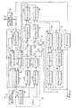
- the device shown in the single figure comprises a transmitting antenna 1 and a receiving antenna 2.
- the transmitting antenna 1 is connected via an antenna box 3 to the output stage of a modulated frequency transmitter 4.
- the frequency modulated stage 4 receives at its input a low frequency signal of amplitude ⁇ ' B (t) emitted by a modulation source not shown.
- a phase shifter 5 is connected by its input to the antenna box 3 and transmits on its outputs a signal in phase with the emission signal to the input of a variable attenuator 6, and a signal in quadrature with the signal d transmission to the input of a variable attenuator 7.
- the output signals of the variable attenuators 6 and 7 are transmitted to the respective inputs E 1 and E 2 of a computing device 8.
- the computing device 8 also receives on its input E 3 the signal received by the receiving antenna 2 and passing through the antenna box 9.
- the computing device 8 is also connected by its outputs S 1 and S 2 to a device 10 separating the AC and DC components making up the output signals of the calculating device 8.
- the outputs S 4 to S 7 of the separating device 10 are respectively connected to the inputs of the control devices 11 to 14.
- the output of the control 11 is connected to an input of an adder 15 which is connected by a second input to the so rtie of the control member 14.
- the output of the control member 12 is connected to an input of an adder 16 whose second input is connected to the output of a control member 13.
- the respective outputs adders 15 and 16 are respectively connected to the control inputs c of the variable attenuators 6 and 7.
- the calculation unit 8 comprises an adder 17, a subtractor 18, two multipliers 19 and 20 as well as filters 21 and 22.
- the adder 17 is connected by its two respective inputs E i and E 2 of the calculating member 8 and by its output to an input of the subtractor 18 whose other input is connected to the input E 3 of the calculation unit 8, the output of the subtractor 18 is connected on the one hand to an input of the multiplier 19 and on the other hand to an input of the multiplier 20.
- the multiplier 19 is connected by a second input at the output of the phase shifter 5 which delivers a quadrature signal with respect to the transmission signal.
- the second input of the multiplier 20 is connected to the output of the phase shifter 5 which delivers a signal in phase with the transmission signal.
- the respective outputs of the multipliers 19 and 20 are connected to the respective inputs of two low-pass filters 21 and 22.
- the respective outputs of the filters 21 and 22 are respectively connected to the outputs Si and S 2 of the calculation unit 8.
- the separator 10 consists of two conductors L, and L 2 respectively connecting the output S 1 of the calculating member 8 to the output S 4 of the separator and the output S 2 of the calculating member 8 to the output S 5 of the separator and by two capacitors Ci and C 2 .
- One end of the capacitor Ci is connected to the conductor L 1 and one end of the capacitor C 2 is connected to the conductor L 2 .
- the other ends of the capacitors Ci and C 2 are connected respectively to the outputs S 6 and S 7 of the attenuator 10.
- the control members 11 and 12 are formed by integrators.
- the control member 13 is constituted by two multipliers 23 and 24 and by an integrator 25.
- An input of the multiplier 23 is connected to the output S 6 of the separator 10 and its other input receives the low frequency signal of frequency modulation of amplitude ⁇ ' B (t).
- An input of the multiplier 24 is connected to the output of the integrator 25 and its other input is connected to the modulation source.
- the integrator 25 has its input connected to the output of the multiplier 23.
- the output of the multiplier 24 is applied to an input of the adder 16.
- the control member 14 comprises two multipliers 26 and 27 and an integrator 28.
- the multiplier 26 is connected by an input to the output S 7 of the separator 10 and by its other input to the modulation source.
- the output of the multiplier 26 is connected to the input of the integrator 28.
- the multiplier 27 is connected by an input to the modulation source delivering the signal ⁇ ' B (t) and by its other input to the output of the integrator 28.
- the output of the multiplier 27 is connected to an input of the adder 15.
- variable attenuators 6 and 7 may be constituted by the P5 ATTL400 attenuators marketed by the Company of the United States of America OLEKTRON and that the phase shifter 5 may be constituted by the component PSCQZ marketed by the Company MINICIRCUIT of the United States of America.
- the interfering signal emitted by the transmitter 4 follows two different paths.
- a first path is constituted by the path followed in the air by the resulting electromagnetic wave between the transmitting antenna 1 and the receiving antenna 2.
- the second path consists of the path of the interfering signal through the electronic antenna decoupling device of the invention.
- the signal emitted by the antenna 1 is a signal modulated in frequency by the low frequency modulation signal of amplitude ⁇ ' B (t) received at the input of the frequency modulated transmitter 4.
- the signal low frequency amplitude ⁇ ' B (t) is transformed inside the transmitter 4 to obtain the phase modulation ⁇ B (t) of the transmission signal.
- This emission signal is therefore represented by equation (7) or
- the signal received by the receiving antenna 2 is composed of a useful signal u (t) and the scrambled signal c '(t) linked by the equation c '(t) being represented by the above equation (1) and the useful signal u (t) having the form where ⁇ u (t) represents the phase or frequency modulation of the useful signal and ⁇ u represents the phase shift of the modulation signal.
- phase shifter 5 delivers two quadrature signals c l (t) and c 2 (t) which can be represented by the equations:
- variable attenuators 6 and 7 deliver on their outputs the signals k 1 c 1 (t) and k 2 c 2 (t). These signals are added in the adder 17 and the result of the addition is subtracted in the subtractor 18 from the signal e (t) received at the input E 3 of the calculation unit 8. The output of the subtractor 18 delivers by therefore a signal:
- the signal e '(t) is multiplied in the multipliers 19 and 20, by the in-phase and quadrature components of the interfering signal c (t) delivered on the outputs of the phase shifter 5.
- the signals e l (t) and e 2 (t) are each composed of a component with zero mean value and a non-zero component. After integration into the integrators 11 and 12, the component with zero mean value disappears and there remain on the outputs S 1 and S 2 of the calculation unit 8 only two error signals e ' 1 (t) and e' 2 (t) which have as equation: and
- the signals e ' 1 (t) and e' 2 (t) can be expressed by involving these constants by the following theoretical developments.
- the continuous components of the signals e i (t) and e 2 (t) are applied respectively to the inputs of the integrators 11 and 12. These continuous components are however blocked at the input of the control members 13 and 14 by the capacitors C 1 and C 2 .
- the alternative components are applied to the respective inputs of the multipliers 23 and 26 which execute a multiplication of these components with the modulation signal ⁇ ' B (t) and which apply the results of the multiplications to the respective inputs of the integrators 25 and 28 which deliver signals whose amplitude is proportional to the signal ⁇ ' B (t).
- the output signals of the integrators 25 and 28 are multiplied again by the signal ⁇ ' B (t) using the multipliers 24 and 27 and the result of this multiplication is transmitted to the respective inputs of the adders 16 and 15.
- the multipliers 24 and 27 have the role of variable gain amplifier, the value of their gain being determined by the amplitude of the signal ⁇ ' B (t).
- the output signals of the multipliers 24 and 27 have an amplitude proportional to this frequency difference.
- the adder 15 delivers an output signal which is equal to the sum of the signals obtained at the output of the integrator 11 and of the control member 14, this signal acts on the control input of the variable attenuator 17 whose attenuation coefficient k 1 will vary so as to cancel the continuous and alternative components of the signal e i (t).
- the output of the adder 16 delivers a signal which is the sum of the signal leaving the integrator 12 and the control member 13, this signal acts on the control of the variable attenuator 6 which evolves so as to cancel the DC and alternative components of the signal e 2 (t).
Landscapes
- Engineering & Computer Science (AREA)
- Computer Networks & Wireless Communication (AREA)
- Signal Processing (AREA)
- Noise Elimination (AREA)
- Radio Relay Systems (AREA)
Applications Claiming Priority (2)
| Application Number | Priority Date | Filing Date | Title |
|---|---|---|---|
| FR8123730 | 1981-12-18 | ||
| FR8123730A FR2518852A1 (fr) | 1981-12-18 | 1981-12-18 | Procede et dispositif electroniques de decouplage d'antenne |
Publications (2)
| Publication Number | Publication Date |
|---|---|
| EP0082756A1 EP0082756A1 (fr) | 1983-06-29 |
| EP0082756B1 true EP0082756B1 (fr) | 1985-02-20 |
Family
ID=9265184
Family Applications (1)
| Application Number | Title | Priority Date | Filing Date |
|---|---|---|---|
| EP82402264A Expired EP0082756B1 (fr) | 1981-12-18 | 1982-12-10 | Procédé et dispositif électroniques de découplage d'antenne |
Country Status (4)
| Country | Link |
|---|---|
| US (1) | US4493111A (enExample) |
| EP (1) | EP0082756B1 (enExample) |
| DE (1) | DE3262461D1 (enExample) |
| FR (1) | FR2518852A1 (enExample) |
Families Citing this family (3)
| Publication number | Priority date | Publication date | Assignee | Title |
|---|---|---|---|---|
| US4776032A (en) * | 1985-05-15 | 1988-10-04 | Nippon Telegraph And Telephone Corporation | Repeater for a same frequency with spillover measurement |
| EP0342277A1 (en) * | 1988-05-16 | 1989-11-23 | Hazeltine Corporation | Tweet elimination, or reduction, in superheterodyne receivers |
| US5428831A (en) * | 1993-01-08 | 1995-06-27 | American Nucleonics Corporation | Signal path length correlator and method and an interference cancellation system using the same |
Family Cites Families (7)
| Publication number | Priority date | Publication date | Assignee | Title |
|---|---|---|---|---|
| US3021521A (en) * | 1955-11-30 | 1962-02-13 | Raytheon Co | Feed-through nulling systems |
| US3155965A (en) * | 1961-04-28 | 1964-11-03 | Raytheon Co | Feed-through nulling system |
| US3699444A (en) * | 1969-02-17 | 1972-10-17 | American Nucleonics Corp | Interference cancellation system |
| US3696429A (en) * | 1971-05-24 | 1972-10-03 | Cutler Hammer Inc | Signal cancellation system |
| US3810182A (en) * | 1971-08-12 | 1974-05-07 | North American Rockwell | Adaptive electronic hybrid transformer |
| DE3110602C2 (de) * | 1980-03-28 | 1985-07-04 | Nippon Telegraph & Telephone Public Corp., Tokio/Tokyo | Interferenz-Kompensationssystem |
| US4423505A (en) * | 1981-11-23 | 1983-12-27 | Loral Corp. | Cued adaptive canceller |
-
1981
- 1981-12-18 FR FR8123730A patent/FR2518852A1/fr active Granted
-
1982
- 1982-12-10 DE DE8282402264T patent/DE3262461D1/de not_active Expired
- 1982-12-10 EP EP82402264A patent/EP0082756B1/fr not_active Expired
- 1982-12-15 US US06/450,008 patent/US4493111A/en not_active Expired - Fee Related
Also Published As
| Publication number | Publication date |
|---|---|
| FR2518852B1 (enExample) | 1984-04-06 |
| FR2518852A1 (fr) | 1983-06-24 |
| US4493111A (en) | 1985-01-08 |
| EP0082756A1 (fr) | 1983-06-29 |
| DE3262461D1 (en) | 1985-03-28 |
Similar Documents
| Publication | Publication Date | Title |
|---|---|---|
| EP0080922B1 (fr) | Dispositif de détection d'impédance optimum de charge d'anode d'un émetteur à tube | |
| FR2670631A1 (fr) | Agencement d'amplificateurs montes en parallele avec moyen de controle des phases et procede d'amplification correspondant. | |
| EP0609435A1 (en) | Apparatus for compensating of phase rotation in a final amplifier stage | |
| FR2741218A1 (fr) | Procede et dispositif d'estimation de non-linearite | |
| EP0483845A2 (en) | Tap weight adaptation control using stepsize inversely variable with signal power level | |
| JPH0527287B2 (enExample) | ||
| FR2517905A1 (fr) | Dispositif d'initialisation pour annuleur d'echo et son application aux echos lointains | |
| EP0082756B1 (fr) | Procédé et dispositif électroniques de découplage d'antenne | |
| JPH0136737B2 (enExample) | ||
| US7010277B1 (en) | Arrangement and method for interference cancelling | |
| EP0722238B1 (fr) | Estimateur d'un défaut de fonctionnement d'un modulateur en quadrature et étage de modulation l'utilisant | |
| EP0696392B1 (fr) | Procede et dispositif de controle automatique de gain de circuits de reception | |
| EP0121446B1 (fr) | Dispositif de linéarisation d'amplificateur haute fréquence à coefficients de non-linéarité complexes | |
| FR2645377A1 (fr) | Circuit suppresseur d'interferences | |
| FR2698502A1 (fr) | Dispositif de récupération du rythme baud dans un récepteur pour modem. | |
| JPH08511929A (ja) | 低中間周波数を有するヘテロダイン受信機 | |
| EP0067091A1 (fr) | Dispositif de correction d'intermodulation produite par un amplificateur de signaux haute fréquence | |
| FR2797957A1 (fr) | Procede et dispositif pour la mesure d'impedance d'antenne | |
| EP0498457A2 (en) | Digital type VSB modulation apparatus | |
| EP0334442B1 (fr) | Annuleur d'écho pour signal d'écho à phase variable | |
| CA2224639A1 (en) | Method, device, dsp and modem for efficient echo canceler phase roll tracking | |
| FR2580448A1 (fr) | Systeme de mise en phase de signaux de telecommunication recus par une antenne adaptative | |
| EP0070236B1 (fr) | Dispositif de compensation de phase d'écho et son application aux annuleurs d'écho | |
| EP0529144A1 (en) | Far-end echo canceller | |
| EP0786887A1 (fr) | Procédé de compensation des différences en temps de propagation de groupe entre les filtres analogiques d'un émetteur ou d'un récepteur de signaux en quadrature de phase |
Legal Events
| Date | Code | Title | Description |
|---|---|---|---|
| PUAI | Public reference made under article 153(3) epc to a published international application that has entered the european phase |
Free format text: ORIGINAL CODE: 0009012 |
|
| AK | Designated contracting states |
Designated state(s): DE GB IT NL |
|
| 17P | Request for examination filed |
Effective date: 19831112 |
|
| RBV | Designated contracting states (corrected) |
Designated state(s): DE GB |
|
| GRAA | (expected) grant |
Free format text: ORIGINAL CODE: 0009210 |
|
| AK | Designated contracting states |
Designated state(s): DE GB |
|
| REF | Corresponds to: |
Ref document number: 3262461 Country of ref document: DE Date of ref document: 19850328 |
|
| PLBE | No opposition filed within time limit |
Free format text: ORIGINAL CODE: 0009261 |
|
| STAA | Information on the status of an ep patent application or granted ep patent |
Free format text: STATUS: NO OPPOSITION FILED WITHIN TIME LIMIT |
|
| 26N | No opposition filed | ||
| REG | Reference to a national code |
Ref country code: GB Ref legal event code: 746 |
|
| PGFP | Annual fee paid to national office [announced via postgrant information from national office to epo] |
Ref country code: DE Payment date: 19921112 Year of fee payment: 11 |
|
| PGFP | Annual fee paid to national office [announced via postgrant information from national office to epo] |
Ref country code: GB Payment date: 19921118 Year of fee payment: 11 |
|
| PG25 | Lapsed in a contracting state [announced via postgrant information from national office to epo] |
Ref country code: GB Effective date: 19931210 |
|
| GBPC | Gb: european patent ceased through non-payment of renewal fee |
Effective date: 19931210 |
|
| PG25 | Lapsed in a contracting state [announced via postgrant information from national office to epo] |
Ref country code: DE Effective date: 19940901 |