EP0082640B1 - Ion implantation method - Google Patents
Ion implantation method Download PDFInfo
- Publication number
- EP0082640B1 EP0082640B1 EP82306568A EP82306568A EP0082640B1 EP 0082640 B1 EP0082640 B1 EP 0082640B1 EP 82306568 A EP82306568 A EP 82306568A EP 82306568 A EP82306568 A EP 82306568A EP 0082640 B1 EP0082640 B1 EP 0082640B1
- Authority
- EP
- European Patent Office
- Prior art keywords
- ion
- ion beam
- region
- wafer
- gate
- Prior art date
- Legal status (The legal status is an assumption and is not a legal conclusion. Google has not performed a legal analysis and makes no representation as to the accuracy of the status listed.)
- Expired
Links
Images


Classifications
-
- H—ELECTRICITY
- H01—ELECTRIC ELEMENTS
- H01L—SEMICONDUCTOR DEVICES NOT COVERED BY CLASS H10
- H01L21/00—Processes or apparatus adapted for the manufacture or treatment of semiconductor or solid state devices or of parts thereof
- H01L21/02—Manufacture or treatment of semiconductor devices or of parts thereof
- H01L21/04—Manufacture or treatment of semiconductor devices or of parts thereof the devices having at least one potential-jump barrier or surface barrier, e.g. PN junction, depletion layer or carrier concentration layer
- H01L21/18—Manufacture or treatment of semiconductor devices or of parts thereof the devices having at least one potential-jump barrier or surface barrier, e.g. PN junction, depletion layer or carrier concentration layer the devices having semiconductor bodies comprising elements of Group IV of the Periodic System or AIIIBV compounds with or without impurities, e.g. doping materials
- H01L21/26—Bombardment with radiation
- H01L21/263—Bombardment with radiation with high-energy radiation
- H01L21/265—Bombardment with radiation with high-energy radiation producing ion implantation
-
- H—ELECTRICITY
- H01—ELECTRIC ELEMENTS
- H01J—ELECTRIC DISCHARGE TUBES OR DISCHARGE LAMPS
- H01J37/00—Discharge tubes with provision for introducing objects or material to be exposed to the discharge, e.g. for the purpose of examination or processing thereof
- H01J37/30—Electron-beam or ion-beam tubes for localised treatment of objects
- H01J37/302—Controlling tubes by external information, e.g. programme control
-
- H—ELECTRICITY
- H01—ELECTRIC ELEMENTS
- H01J—ELECTRIC DISCHARGE TUBES OR DISCHARGE LAMPS
- H01J37/00—Discharge tubes with provision for introducing objects or material to be exposed to the discharge, e.g. for the purpose of examination or processing thereof
- H01J37/30—Electron-beam or ion-beam tubes for localised treatment of objects
- H01J37/317—Electron-beam or ion-beam tubes for localised treatment of objects for changing properties of the objects or for applying thin layers thereon, e.g. for ion implantation
- H01J37/3171—Electron-beam or ion-beam tubes for localised treatment of objects for changing properties of the objects or for applying thin layers thereon, e.g. for ion implantation for ion implantation
- H01J37/3172—Maskless patterned ion implantation
-
- Y—GENERAL TAGGING OF NEW TECHNOLOGICAL DEVELOPMENTS; GENERAL TAGGING OF CROSS-SECTIONAL TECHNOLOGIES SPANNING OVER SEVERAL SECTIONS OF THE IPC; TECHNICAL SUBJECTS COVERED BY FORMER USPC CROSS-REFERENCE ART COLLECTIONS [XRACs] AND DIGESTS
- Y10—TECHNICAL SUBJECTS COVERED BY FORMER USPC
- Y10S—TECHNICAL SUBJECTS COVERED BY FORMER USPC CROSS-REFERENCE ART COLLECTIONS [XRACs] AND DIGESTS
- Y10S438/00—Semiconductor device manufacturing: process
- Y10S438/961—Ion beam source and generation
Definitions
- the present invention relates to an ion implantation method of implanting ions into a semiconductor wafer to form at least one of gate, source, drain and field regions of transistors according to the pre-characterizing part of claim 1.
- Such a method is known from J. Vac. Sci. Techno!. Vol. 12, No. 6, Nov/Dec 1975, pages 1378-1381.
- Ion implantation is a very important technique and is widely used in the manufacture of semiconductor devices.
- Si-MOS-LSI silicon metal oxide semiconductor large scale integration
- ion implantation is used for controlling the threshold voltage V TH for formation of well regions, isolation regions, source and drain regions and the like; and for prevention of the punch-through phenomenon.
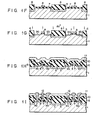
- Figs. 1A to 11 are sectional views showing a conventional Si-MOS-LSI during various manufacturing steps using conventional ion implantation techniques.
- a silicon wafer 1 is annealed in an oxygen atmosphere at 1,000°C for 20 minutes to form a silicon oxide (SiO z ) film 2 of 50 nm (500 A) thickness.
- a silicon nitride film 3 is deposited on the silicon oxide film 2 to a thickness of about 400 nm (4,000 A).
- a resist on the silicon nitride (Si 3 N 4 ) film 3 After coating a resist on the silicon nitride (Si 3 N 4 ) film 3, it is patterned by general lithography to form resist patterns 4. Then, as shown in Fig. 1 C, the silicon nitride film 3 is etched using the resist patterns 4 as a mask. Ion implantation of boron (B + ) is performed at an acceleration voltage of 100 keV to form a p +- type layer 5 for element isolation. Referring to Fig. 1 D, after removing the resist patterns 4, field oxide films 6 of 1 pm thickness are formed in an oxygen atmosphere at 1,000°C and the silicon nitride film 3 is removed thereafter. As shown in Fig.
- a gate oxide film 7 of about 30 nm (300 A) thickness is formed. Boron ions (B + ) are uniformly implanted at an acceleration voltage of 70 keV for the purpose of controlling the threshold voltage VTH.
- Fig. 1F after depositing a polysilicon film of about 300 nm (3,000 A) thickness over the entire surface of the structure, it is subjected to lithography and etching to form polysilicon gates 8. Subsequently, as shown in Fig. 1 G, the gate oxide film 7 is etched to leave only those portions below the polysilicon gates 8.
- arsenic ions are implanted at an acceleration voltage of 100 keV to form source regions 9a and drain regions 9b.
- a phosphate glass film 11 is deposited on the insulating oxide film 10 to a thickness of 700 nm (7,000 A).
- the phosphate glass film 11 is heated in a nitrogen atmosphere at about 1,000°C to smoothen its surface.
- Contact holes are then formed by lithography and etching.
- An Si-MOS-LSI as shown in Fig. 11 is finally manufactured.
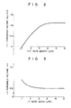
- lon implantation adopted in the manufacture of the Si-MOS-LSI described above is uniform ion implantation in each case.
- MOS transistors manufactured by such a method have variations in the threshold voltage VTH according to the gate lengths and widths thereof.
- Fig. 2 is a graph showing the threshold voltage V TH as a function of gate length.
- Fig. 3 is a graph showing the threshold voltage V TH as a function of gate width.
- an ion implantation apparatus comprising an ion gun for producing an ion beam, an ion optical system for producing a focus spot of the beam on a semiconductor wafer on which transistors are to be formed, a deflecting device for deflecting the ion beam to scan the wafer, a blanking device for blanking the ion beam, and a controller for controlling the deflecting device and the blanking device.
- the transistors are intended to have gate, source, drain and field regions.
- the controller stores data of ion devices intended to be implanted into the wafer as a function of their location on the wafer and controls the beam in accordance with the ion dose data it has stored therein.
- the implantation dose profile is tailored by controlling the rate of sweeps per line.
- a micro ion beam of B + , P + or As+ of high luminance from a eutectic alloy liquid metal ion source has recently been made available. It is also known that the threshold voltage V TH of a transistor depends upon the gate length and width as well as on the ion concentration of the gate region.
- an ion implantation method of implanting ions into a semiconductor wafer to form at least one of gate, source, drain and field regions of transistors having small gate lengths and widths uses an ion implantation apparatus comprising an ion gun for producing an ion beam; an ion optical system for producing a focused spot of the beam on said wafer; the ion beam focused on said wafer having a spot diameter smaller than a continuous semiconductor region into which ions are to be implanted; a deflecting device for deflecting the ion beam to scan said wafer on which said transistors are to be formed; a blanking device for blanking the ion beam; and a controller for controlling said deflecting device and said blanking device, said controller being arranged to store data of ion doses to be implanted into said wafer as a function of location on said wafer and control the ion beam in accordance with the ion dose data stored therein, characterized in that:
- the threshold voltage of the transistor may be easily and precisely controlled. Moreover, the problems of the punch-through phenomenon, the short channel effect and the narrow channel effect usually found in micronized transistors having sizes in the order of submicrons may be prevented.
- the present invention is extremely useful for the manufacture of various types of semiconductor devices including micronized transistors.
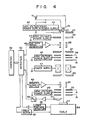
- Fig. 4 is a schematic block diagram of a micro ion beam scanner which is used in accordance with an embodiment of the present invention.
- reference numeral 21 denotes a filament for holding and heating a liquid metal; 22, an emitter; 23, a B-Pt-Au-Ge-type liquid metal alloy reservoir; 24, ion drawing electrodes; and 25, grid electrodes. These parts together form an ion gun for emitting a micro ion beam.
- Blanking electrodes 26 are for turning the ion beam ON/ OFF.
- a blanking aperture mask 27 is for blanking the ion beam.
- Electrostatic lenses or condenser lenses 28 of Einzel type serve to focus the ion beam.
- Reference numeral 29 denotes the deflection coil of a mass analyzer of.
- An ion selection aperture mask 30 is for selecting the type of ions to be implanted.
- a deflector 31 scans the ion beam on a specimen surface.
- Electrostatic lenses or objective lenses 32 are also of Einzel type.
- a specimen 33 for example, a silicon wafer, is securely held on a specimen table 34.
- a drive motor 35 drives the specimen table 34 and a laser position detector 36 detects the position of the specimen table 34.
- a reflected ion detector 37 is used for registration.
- An A/D converter 38 converts an analog reflected ion signal from the detector 37 into a digital signal.
- a computer 39 performs various types of control operations and is connected to an interface 40.
- a heating power supply 41 is used to supply power to the filament 21.
- a high voltage power supply 42 is used to supply power to the ion gun.
- a bias power supply 43 is used to drive the grid electrodes 25.
- a high voltage power supply 44 is used to drive the ion drawing electrodes 24.
- a pattern signal generator 45 converts a pattern signal from the computer 39 into an analog signal.
- a high voltage power supply 46 is used to supply power to the condenser lenses 28.
- a power supply 47 is used to produce an electric field and a magnetic field of the mass analyzer 29.
- a deflection power supply 48 is used to supply power to the deflector 31.
- a high voltage power supply 49 is used to supply power to the objective lenses 32.
- the micro ion beam scanner of the configuration as described above is similar to that of a known electron beam scanner, for example, as disclosed in US-A-4063103.
- Ions emitted from the emitter 22 are composite ions containing 32% of B + ions, for example.
- the B + ions alone are selected from the composite ions by the mass analyzer 29 and the ion selection aperture mask 30 and are focused on the specimen 33 by the objective lenses 32.
- the luminance of the ion gun is 1 x10 6 (A/cm 2 ⁇ str) and the diameter of the ion beam is variable within the range of 0.5 to 0.1 p.
- An ion dose of 10 11 to 10" (ions/cm 2 ) is required for the purpose of controlling the threshold voltage V TH of a transistor. Therefore, in the case of a silicon wafer having a diameter of 10.16 cm (4 inches) and an ion beam having the spot diameter of 0.5 pm, the ion implantation time is about 5 minutes.
- Fig. 5 is a graph showing the threshold voltage V TH as a function of ion dose; they hold a linear relation.
- the threshold voltage V TH of a MOS transistor with gate length and width being 3 pm or less is expressed by: where L is the gate length, W is the gate width and D is the ion dose.
- the threshold voltage V TH may be controlled by storing equation (1) in the computer 39 and varying the ion dose in accordance with the gate dimensions (length and width).
- the ion dose within a silicon wafer surface may be changed in thefollowing manner. Assumethatthe ion beam is OFF (blanked) when voltage Vo is applied to the blanking electrodes 26.
- the deflection voltage has a stepped waveform as shown in Fig. 6B so as to scan the ion beam in a stepped form.
- the pulse width of the blanking voltage or signal being variable in units of (1/10)At.
- the ion beam ON time is (9/10)At at locations x2, x3 and x4.
- the ion beam ON time is (5/10)At at locations x7, x8 and x9. In this manner, the ion dose may be varied in ten steps at any location.
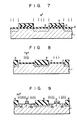
- micro ion beam scanner as described above is used to manufacture an Si-MOS-LSI according to the method of the present invention.
- a micro ion beam scanner as shown in Fig. 4 for implantation of B + ions and another micro ion beam scanner for implantation of As+ ions are prepared; both can vary acceleration voltages.
- B + ions are implanted only into a p +- type layer 5 as the field region, as shown in Fig. 7.
- the acceleration voltage of B + ions is adjusted to 100 keV so as to implant B + ions in the regions surrounding the p +- type layer 5 at a lower dose than that for the p +- type layer 5, those regions being regions close to prospective source and drain regions (9a and 9b) and also regions at the boundary between the field regions and channel regions below the gates. This prevents the narrow channel effect of the transistors, to facilitate micronization thereof.
- B + ions are implanted only into the prospective gate regions, as shown in Fig. 8.
- the acceleration voltage of B + ions at this time is controlled to be 70 keV; the ion dose is increased with a decrease in the gate length.
- the threshold voltage V TH can be easily ⁇ ontrolled even in the manufacture of a micronized transistor having a gate length of 3 ⁇ m or less.
- the position control of the ion beam with respect to the gate can be performed with high precision by detecting the reflected ions from a mark formed within an LSI chip by the reflected ion detector.
- As+ ions are implanted only into source and drain regions 9a and 9b, as shown in Fig. 9.
- the acceleration voltage of As+ ions is controlled to be 100 keV.
- the ion dose in a portion of the drain region 9b near the gate region is controlled to be higher than that in the remaining regions. Thus, the punch-through phenomenon is prevented, to facilitate micronization of the transistors.
- the present invention is not limited to the particular embodiment described above.
- the ions to be implanted are not limited to B + or As+ ions but may include ions of liquid metals such as Si + , Ga + , Se + , or P + ions which are required in the semiconductor industry.
- the method of the present invention is not limited to the manufacture of Si-MOS-LSIs but may be extended to various other types of FET semiconductor devices.
- the spot of the ion beam need not have a circular shape and may have any appropriate shape as determined by the beam shaping aperture mask.
- the electron gun as the ion gun need not be a liquid metal ion gun but may be of any type as long as it has high luminance, for example, of a gas electric field ionization type. This is because if the luminance is about 1 ⁇ 10 3 (A/ cm2. str) or below, the time required for ion implantation becomes enormously long.
Description
- The present invention relates to an ion implantation method of implanting ions into a semiconductor wafer to form at least one of gate, source, drain and field regions of transistors according to the pre-characterizing part of
claim 1. Such a method is known from J. Vac. Sci. Techno!. Vol. 12, No. 6, Nov/Dec 1975, pages 1378-1381. - Ion implantation is a very important technique and is widely used in the manufacture of semiconductor devices. For example, in silicon metal oxide semiconductor large scale integration (to be referred to as Si-MOS-LSI), ion implantation is used for controlling the threshold voltage VTH for formation of well regions, isolation regions, source and drain regions and the like; and for prevention of the punch-through phenomenon.
- In conventional ion implantation techniques, ions are in most cases uniformly implanted into a silicon wafer as will be described hereinafter. Figs. 1A to 11 are sectional views showing a conventional Si-MOS-LSI during various manufacturing steps using conventional ion implantation techniques. Referring to Fig. 1 A first, a
silicon wafer 1 is annealed in an oxygen atmosphere at 1,000°C for 20 minutes to form a silicon oxide (SiOz)film 2 of 50 nm (500 A) thickness. Next, referring to Fig. 1B, asilicon nitride film 3 is deposited on thesilicon oxide film 2 to a thickness of about 400 nm (4,000 A). After coating a resist on the silicon nitride (Si3N4)film 3, it is patterned by general lithography to formresist patterns 4. Then, as shown in Fig. 1 C, thesilicon nitride film 3 is etched using theresist patterns 4 as a mask. Ion implantation of boron (B+) is performed at an acceleration voltage of 100 keV to form a p+-type layer 5 for element isolation. Referring to Fig. 1 D, after removing theresist patterns 4,field oxide films 6 of 1 pm thickness are formed in an oxygen atmosphere at 1,000°C and thesilicon nitride film 3 is removed thereafter. As shown in Fig. 1 E, after removing thesilicon oxide film 2, agate oxide film 7 of about 30 nm (300 A) thickness is formed. Boron ions (B+) are uniformly implanted at an acceleration voltage of 70 keV for the purpose of controlling the threshold voltage VTH. Referring to Fig. 1F, after depositing a polysilicon film of about 300 nm (3,000 A) thickness over the entire surface of the structure, it is subjected to lithography and etching to formpolysilicon gates 8. Subsequently, as shown in Fig. 1 G, thegate oxide film 7 is etched to leave only those portions below thepolysilicon gates 8. In this state, arsenic ions (As+) are implanted at an acceleration voltage of 100 keV to formsource regions 9a anddrain regions 9b. Referring to Fig. 1H, after depositing an insulating oxide film (Si02) 10 of 500 nm (5000 A) thickness over the entire surface of the structure, aphosphate glass film 11 is deposited on theinsulating oxide film 10 to a thickness of 700 nm (7,000 A). Thephosphate glass film 11 is heated in a nitrogen atmosphere at about 1,000°C to smoothen its surface. Contact holes are then formed by lithography and etching. After depositing an aluminum film, it is patterned to formaluminum wiring patterns 12. An Si-MOS-LSI as shown in Fig. 11 is finally manufactured. - lon implantation adopted in the manufacture of the Si-MOS-LSI described above is uniform ion implantation in each case. MOS transistors manufactured by such a method have variations in the threshold voltage VTH according to the gate lengths and widths thereof. Fig. 2 is a graph showing the threshold voltage VTH as a function of gate length. Fig. 3 is a graph showing the threshold voltage VTH as a function of gate width. As may be seen from these graphs, with decreases in either the gate length or width of the transistors, or with micronization of the transistors, control of the threshold voltage VTH becomes difficult due to the short channel effect and the narrow channel effet. Furthermore, the problem of the punch-through phenomenon becomes more pronounced with micronization of the transistors.
- Journal of Vacuum Science and Technology, Vol. 12, No. 6 November/December 1975, pages 1378-1381 discloses an ion implantation apparatus comprising an ion gun for producing an ion beam, an ion optical system for producing a focus spot of the beam on a semiconductor wafer on which transistors are to be formed, a deflecting device for deflecting the ion beam to scan the wafer, a blanking device for blanking the ion beam, and a controller for controlling the deflecting device and the blanking device. The transistors are intended to have gate, source, drain and field regions. The controller stores data of ion devices intended to be implanted into the wafer as a function of their location on the wafer and controls the beam in accordance with the ion dose data it has stored therein. In this known implantation method the implantation dose profile is tailored by controlling the rate of sweeps per line.
- It is an object of the present invention to provide an ion implantation method for the manufacture of semiconductor devices, wherein a threshold voltage VTH of a transistor may be easily and precisely controlled, and problems of the short channel effect, the narrow channel effect and the punch-through phenomenon generally encountered with micronization of transistors may be prevented.
- A micro ion beam of B+, P+ or As+ of high luminance from a eutectic alloy liquid metal ion source has recently been made available. It is also known that the threshold voltage VTH of a transistor depends upon the gate length and width as well as on the ion concentration of the gate region.
- According to the present invention, there is provided an ion implantation method of implanting ions into a semiconductor wafer to form at least one of gate, source, drain and field regions of transistors having small gate lengths and widths, and which uses an ion implantation apparatus comprising an ion gun for producing an ion beam; an ion optical system for producing a focused spot of the beam on said wafer; the ion beam focused on said wafer having a spot diameter smaller than a continuous semiconductor region into which ions are to be implanted; a deflecting device for deflecting the ion beam to scan said wafer on which said transistors are to be formed; a blanking device for blanking the ion beam; and a controller for controlling said deflecting device and said blanking device, said controller being arranged to store data of ion doses to be implanted into said wafer as a function of location on said wafer and control the ion beam in accordance with the ion dose data stored therein, characterized in that:
- the deflection voltage is applied in stepped waveform and that during the time period for which the deflection voltage is kept constant so that the ion beam stays at a given spot location the pulse width of the blanking voltage is controlled in order to variably control the irradiation time of the ion beam on said given spot location within said semiconductor region in accordance with the ion dose data for this spot location stored in said controller.
- Since the ion concentration is varied in accordance with a given spot location into which ions are to be implanted according to the present invention, the threshold voltage of the transistor may be easily and precisely controlled. Moreover, the problems of the punch-through phenomenon, the short channel effect and the narrow channel effect usually found in micronized transistors having sizes in the order of submicrons may be prevented. The present invention is extremely useful for the manufacture of various types of semiconductor devices including micronized transistors.
- By way of example and to make the description clearer, reference is made to the accompanying drawings in which:
- Figs. 1A to 11 are sectional views showing a conventional Si-MOS-LSI in various manufacturing steps using ion implantation;
- Fig. 2 is a graph showing the threshold voltage VTH as a function of gate length for the MOS transistor manufactured by the steps shown in Figs. 1A to 11;
- Fig. 3 is a graph showing the threshold voltage VTH as a function of gate width for the MOS transistor manufactured by the steps shown in Figs. 1A to 11;
- Fig. 4 is a schematic block diagram of a micro ion beam scanner used in accordance with one embodiment of the present invention;
- Fig. 5 is a graph showing the threshold voltage VTH as a function of the B+ ion dose for the MOS transistor manufactured by the scanner shown in Fig. 4;
- Figs. 6A to 6C are representations for explaining the process for varying the ion does according to the present invention; and
- Figs. 7 to 9 are sectional views for explaining the ion implantation steps according to an embodiment of the present invention.
- The preferred embodiment of the present invention will now be described in detail with reference to the accompanying drawings.
- Fig. 4 is a schematic block diagram of a micro ion beam scanner which is used in accordance with an embodiment of the present invention. Referring to Fig. 4,
reference numeral 21 denotes a filament for holding and heating a liquid metal; 22, an emitter; 23, a B-Pt-Au-Ge-type liquid metal alloy reservoir; 24, ion drawing electrodes; and 25, grid electrodes. These parts together form an ion gun for emitting a micro ion beam. Blanking electrodes 26 are for turning the ion beam ON/ OFF. A blanking aperture mask 27 is for blanking the ion beam. Electrostatic lenses orcondenser lenses 28 of Einzel type serve to focus the ion beam.Reference numeral 29 denotes the deflection coil of a mass analyzer of. An ionselection aperture mask 30 is for selecting the type of ions to be implanted. A deflector 31 scans the ion beam on a specimen surface. Electrostatic lenses orobjective lenses 32 are also of Einzel type. Aspecimen 33, for example, a silicon wafer, is securely held on a specimen table 34. Adrive motor 35 drives the specimen table 34 and alaser position detector 36 detects the position of the specimen table 34. A reflected ion detector 37 is used for registration. An A/D converter 38 converts an analog reflected ion signal from the detector 37 into a digital signal. Acomputer 39 performs various types of control operations and is connected to aninterface 40. Aheating power supply 41 is used to supply power to thefilament 21. A highvoltage power supply 42 is used to supply power to the ion gun. Abias power supply 43 is used to drive thegrid electrodes 25. A highvoltage power supply 44 is used to drive theion drawing electrodes 24. Apattern signal generator 45 converts a pattern signal from thecomputer 39 into an analog signal. A highvoltage power supply 46 is used to supply power to thecondenser lenses 28. Apower supply 47 is used to produce an electric field and a magnetic field of themass analyzer 29. Adeflection power supply 48 is used to supply power to the deflector 31. A highvoltage power supply 49 is used to supply power to theobjective lenses 32. - The micro ion beam scanner of the configuration as described above is similar to that of a known electron beam scanner, for example, as disclosed in US-A-4063103. Ions emitted from the emitter 22 are composite ions containing 32% of B+ ions, for example. The B+ ions alone are selected from the composite ions by the
mass analyzer 29 and the ionselection aperture mask 30 and are focused on thespecimen 33 by theobjective lenses 32. The luminance of the ion gun is 1 x10⁶ (A/cm2 · str) and the diameter of the ion beam is variable within the range of 0.5 to 0.1 p. An ion dose of 1011 to 10" (ions/cm2) is required for the purpose of controlling the threshold voltage VTH of a transistor. Therefore, in the case of a silicon wafer having a diameter of 10.16 cm (4 inches) and an ion beam having the spot diameter of 0.5 pm, the ion implantation time is about 5 minutes. - Fig. 5 is a graph showing the threshold voltage VTH as a function of ion dose; they hold a linear relation. As may be seen from Figs. 2 and 3, the threshold voltage VTH of a MOS transistor with gate length and width being 3 pm or less is expressed by:

computer 39 and varying the ion dose in accordance with the gate dimensions (length and width). The ion dose within a silicon wafer surface may be changed in thefollowing manner. Assumethatthe ion beam is OFF (blanked) when voltage Vo is applied to the blanking electrodes 26. Assume also that the deflection voltage has a stepped waveform as shown in Fig. 6B so as to scan the ion beam in a stepped form. Let At stand for a time period for which the ion beam stays at a given location xn, the pulse width of the blanking voltage or signal being variable in units of (1/10)At. When the blanking voltage changes as shown in Fig. 6A, the ion beam is OFF at locations x0, x1, x5 and x6 as shown in Fig. 6C. The ion beam ON time is (9/10)At at locations x2, x3 and x4. The ion beam ON time is (5/10)At at locations x7, x8 and x9. In this manner, the ion dose may be varied in ten steps at any location. - An example will be described wherein the micro ion beam scanner as described above is used to manufacture an Si-MOS-LSI according to the method of the present invention. First, a micro ion beam scanner as shown in Fig. 4 for implantation of B+ ions and another micro ion beam scanner for implantation of As+ ions are prepared; both can vary acceleration voltages. In place of the step for implanting B+ ions shown in Fig. 1 C, B+ ions are implanted only into a p+-type layer 5 as the field region, as shown in Fig. 7. Then, the acceleration voltage of B+ ions is adjusted to 100 keV so as to implant B+ ions in the regions surrounding the p+- type layer 5 at a lower dose than that for the p+- type layer 5, those regions being regions close to prospective source and drain regions (9a and 9b) and also regions at the boundary between the field regions and channel regions below the gates. This prevents the narrow channel effect of the transistors, to facilitate micronization thereof.
- In place of the step of implanting B+ ions shown in Fig. 1E, B+ ions are implanted only into the prospective gate regions, as shown in Fig. 8. The acceleration voltage of B+ ions at this time is controlled to be 70 keV; the ion dose is increased with a decrease in the gate length. With these measures, the threshold voltage VTH can be easily ëontrolled even in the manufacture of a micronized transistor having a gate length of 3 µm or less. The position control of the ion beam with respect to the gate can be performed with high precision by detecting the reflected ions from a mark formed within an LSI chip by the reflected ion detector.
- In place ofthestep of implanting As+ ions shown in Fig. 1G, As+ ions are implanted only into source and
drain regions drain region 9b near the gate region is controlled to be higher than that in the remaining regions. Thus, the punch-through phenomenon is prevented, to facilitate micronization of the transistors. - In Si-MOS-LSIs manufactured in this manner, even when the gate length and width were 3 µm or less, the threshold voltage VTH was easily controlled to remain at the standard value. High reliability was obtained without causing the narrow channel effect or the punch-through phenomenon.
- The present invention is not limited to the particular embodiment described above. For example, the ions to be implanted are not limited to B+ or As+ ions but may include ions of liquid metals such as Si+, Ga+, Se+, or P+ ions which are required in the semiconductor industry. Then, the method of the present invention is not limited to the manufacture of Si-MOS-LSIs but may be extended to various other types of FET semiconductor devices. The spot of the ion beam need not have a circular shape and may have any appropriate shape as determined by the beam shaping aperture mask. The electron gun as the ion gun need not be a liquid metal ion gun but may be of any type as long as it has high luminance, for example, of a gas electric field ionization type. This is because if the luminance is about 1 × 10³ (A/ cm2. str) or below, the time required for ion implantation becomes enormously long.
Claims (5)
Applications Claiming Priority (2)
| Application Number | Priority Date | Filing Date | Title |
|---|---|---|---|
| JP205015/81 | 1981-12-18 | ||
| JP56205015A JPS58106823A (en) | 1981-12-18 | 1981-12-18 | Ion implantation |
Publications (3)
| Publication Number | Publication Date |
|---|---|
| EP0082640A2 EP0082640A2 (en) | 1983-06-29 |
| EP0082640A3 EP0082640A3 (en) | 1984-08-22 |
| EP0082640B1 true EP0082640B1 (en) | 1987-10-14 |
Family
ID=16500029
Family Applications (1)
| Application Number | Title | Priority Date | Filing Date |
|---|---|---|---|
| EP82306568A Expired EP0082640B1 (en) | 1981-12-18 | 1982-12-09 | Ion implantation method |
Country Status (4)
| Country | Link |
|---|---|
| US (1) | US4481042A (en) |
| EP (1) | EP0082640B1 (en) |
| JP (1) | JPS58106823A (en) |
| DE (1) | DE3277479D1 (en) |
Families Citing this family (17)
| Publication number | Priority date | Publication date | Assignee | Title |
|---|---|---|---|---|
| JPS60143630A (en) * | 1983-12-29 | 1985-07-29 | Fujitsu Ltd | Ion implantation |
| JPS61140175A (en) * | 1984-12-13 | 1986-06-27 | Semiconductor Energy Lab Co Ltd | Manufacture of semiconductor device |
| US6784033B1 (en) | 1984-02-15 | 2004-08-31 | Semiconductor Energy Laboratory Co., Ltd. | Method for the manufacture of an insulated gate field effect semiconductor device |
| JPS60243960A (en) * | 1984-05-18 | 1985-12-03 | Hitachi Ltd | Ion microbeam device |
| JP2597976B2 (en) * | 1985-03-27 | 1997-04-09 | 株式会社東芝 | Semiconductor device and manufacturing method thereof |
| JPS61237421A (en) * | 1985-04-15 | 1986-10-22 | Hitachi Ltd | Manufacture of semiconductor device |
| FR2592224B1 (en) * | 1985-12-20 | 1988-10-07 | Thomson Csf | FIELD EFFECT TRANSISTOR, AND LOGIC INTEGRATED CIRCUIT COMPRISING SUCH A TRANSISTOR |
| FR2592225B1 (en) * | 1985-12-20 | 1988-02-05 | Thomson Csf | POWER HYPERFREQUENCY TRANSISTOR |
| US4746964A (en) * | 1986-08-28 | 1988-05-24 | Fairchild Semiconductor Corporation | Modification of properties of p-type dopants with other p-type dopants |
| US5256579A (en) * | 1989-04-03 | 1993-10-26 | Massachusetts Institute Of Technology | Tunable-frequency Gunn diodes fabrication with focused ion beams |
| DE4339190B4 (en) * | 1992-11-16 | 2006-04-13 | Denso Corp., Kariya | Semiconductor accelerometer |
| JP2000040691A (en) * | 1998-07-21 | 2000-02-08 | Oki Electric Ind Co Ltd | Manufacture of semiconductor device |
| KR100546334B1 (en) * | 2003-07-01 | 2006-01-26 | 삼성전자주식회사 | Integrated circuit semiconductor device having different impurity concentration in respective regions of a semiconductor wafer, and fabrication method thereof |
| US7425353B2 (en) * | 2004-01-29 | 2008-09-16 | International Business Machines Corporation | Enhancement of magnetic media recording performance using ion irradiation to tailor exchange coupling |
| US20070195482A1 (en) * | 2006-02-23 | 2007-08-23 | Varian Semiconductor Equipment Associates, Inc. | Johnsen-Rahbek electrostatic chuck driven with AC voltage |
| KR200466175Y1 (en) * | 2011-06-13 | 2013-04-03 | 백미정 | a coil spring join structure for playground |
| CN104538457A (en) * | 2015-01-15 | 2015-04-22 | 京东方科技集团股份有限公司 | Thin film transistor, manufacturing method of thin film transistor, array substrate and display device |
Family Cites Families (4)
| Publication number | Priority date | Publication date | Assignee | Title |
|---|---|---|---|---|
| CA953823A (en) * | 1971-08-24 | 1974-08-27 | Western Electric Company, Incorporated | Ion beam control apparatus |
| US4063103A (en) * | 1975-04-11 | 1977-12-13 | Tokyo Shibaura Electric Co., Ltd. | Electron beam exposure apparatus |
| FR2412939A1 (en) * | 1977-12-23 | 1979-07-20 | Anvar | HIGH CURRENT ION IMPLANTER |
| US4283631A (en) * | 1980-02-22 | 1981-08-11 | Varian Associates, Inc. | Bean scanning and method of use for ion implantation |
-
1981
- 1981-12-18 JP JP56205015A patent/JPS58106823A/en active Granted
-
1982
- 1982-12-08 US US06/448,048 patent/US4481042A/en not_active Expired - Lifetime
- 1982-12-09 EP EP82306568A patent/EP0082640B1/en not_active Expired
- 1982-12-09 DE DE8282306568T patent/DE3277479D1/en not_active Expired
Also Published As
| Publication number | Publication date |
|---|---|
| US4481042A (en) | 1984-11-06 |
| JPS643048B2 (en) | 1989-01-19 |
| EP0082640A3 (en) | 1984-08-22 |
| DE3277479D1 (en) | 1987-11-19 |
| JPS58106823A (en) | 1983-06-25 |
| EP0082640A2 (en) | 1983-06-29 |
Similar Documents
| Publication | Publication Date | Title |
|---|---|---|
| EP0082640B1 (en) | Ion implantation method | |
| EP0082639B1 (en) | Processing method using a focused ion beam | |
| US5661043A (en) | Forming a buried insulator layer using plasma source ion implantation | |
| KR100388731B1 (en) | Method of manufacturing a semiconductor device | |
| US7638782B2 (en) | Semiconductor device manufacturing method and ion implanter used therein | |
| EP0097533B1 (en) | A method of manufacturing a mis type semiconductor device | |
| EP0165055B1 (en) | Method and apparatus for exposing photoresist by using an electron beam and controlling its voltage and charge | |
| US6355574B1 (en) | Method and device for treating a semiconductor surface | |
| US20020185948A1 (en) | Method for fabricating tiny field emitter tips | |
| JPS6142850B2 (en) | ||
| US5286978A (en) | Method of removing electric charge accumulated on a semiconductor substrate in ion implantation | |
| US20030211711A1 (en) | Wafer processing method and ion implantation apparatus | |
| US6191012B1 (en) | Method for forming a shallow junction in a semiconductor device using antimony dimer | |
| Downey et al. | Control of BF2 dissociation in high-current ion implantation | |
| EP0424925B1 (en) | Method of removing electric charge accumulated on a semiconductor substrate in ion implantation | |
| JPS58223321A (en) | Implantation of ion | |
| EP1495479A1 (en) | Emitter with filled zeolite emission layer | |
| JP3175280B2 (en) | Ion implantation method | |
| JP4083104B2 (en) | Process for doping the pattern of a resistive element | |
| JPH1174232A (en) | Film-patterning method | |
| JP3057808B2 (en) | Ion implanter | |
| JPH05211328A (en) | Mos transistor and manufacturing method thereof | |
| JPS59202628A (en) | Manufacture of semiconductor device | |
| Current et al. | Status Of The Production Use Of Ion Implantation For IC Manufacture And Requirements For Competitive Application Of Focused Ion Beams | |
| JPS6132433A (en) | Manufacture of semiconductor device |
Legal Events
| Date | Code | Title | Description |
|---|---|---|---|
| PUAI | Public reference made under article 153(3) epc to a published international application that has entered the european phase |
Free format text: ORIGINAL CODE: 0009012 |
|
| 17P | Request for examination filed |
Effective date: 19821217 |
|
| AK | Designated contracting states |
Designated state(s): DE FR GB IT |
|
| PUAL | Search report despatched |
Free format text: ORIGINAL CODE: 0009013 |
|
| RHK1 | Main classification (correction) |
Ipc: H01L 21/265 |
|
| AK | Designated contracting states |
Designated state(s): DE FR GB IT |
|
| RAP1 | Party data changed (applicant data changed or rights of an application transferred) |
Owner name: KABUSHIKI KAISHA TOSHIBA |
|
| GRAA | (expected) grant |
Free format text: ORIGINAL CODE: 0009210 |
|
| AK | Designated contracting states |
Kind code of ref document: B1 Designated state(s): DE GB |
|
| REF | Corresponds to: |
Ref document number: 3277479 Country of ref document: DE Date of ref document: 19871119 |
|
| PLBE | No opposition filed within time limit |
Free format text: ORIGINAL CODE: 0009261 |
|
| STAA | Information on the status of an ep patent application or granted ep patent |
Free format text: STATUS: NO OPPOSITION FILED WITHIN TIME LIMIT |
|
| 26N | No opposition filed | ||
| PGFP | Annual fee paid to national office [announced via postgrant information from national office to epo] |
Ref country code: GB Payment date: 19961202 Year of fee payment: 15 |
|
| PGFP | Annual fee paid to national office [announced via postgrant information from national office to epo] |
Ref country code: DE Payment date: 19961216 Year of fee payment: 15 |
|
| PG25 | Lapsed in a contracting state [announced via postgrant information from national office to epo] |
Ref country code: GB Free format text: LAPSE BECAUSE OF NON-PAYMENT OF DUE FEES Effective date: 19971209 |
|
| GBPC | Gb: european patent ceased through non-payment of renewal fee |
Effective date: 19971209 |
|
| PG25 | Lapsed in a contracting state [announced via postgrant information from national office to epo] |
Ref country code: DE Free format text: LAPSE BECAUSE OF NON-PAYMENT OF DUE FEES Effective date: 19980901 |