EP0081224A2 - Circuit arrangement for the addressing of different memory units in a micro computer system - Google Patents
Circuit arrangement for the addressing of different memory units in a micro computer system Download PDFInfo
- Publication number
- EP0081224A2 EP0081224A2 EP82111269A EP82111269A EP0081224A2 EP 0081224 A2 EP0081224 A2 EP 0081224A2 EP 82111269 A EP82111269 A EP 82111269A EP 82111269 A EP82111269 A EP 82111269A EP 0081224 A2 EP0081224 A2 EP 0081224A2
- Authority
- EP
- European Patent Office
- Prior art keywords
- memory
- address
- bus
- circuit arrangement
- read
- Prior art date
- Legal status (The legal status is an assumption and is not a legal conclusion. Google has not performed a legal analysis and makes no representation as to the accuracy of the status listed.)
- Withdrawn
Links
Images
Classifications
-
- G—PHYSICS
- G06—COMPUTING; CALCULATING OR COUNTING
- G06F—ELECTRIC DIGITAL DATA PROCESSING
- G06F12/00—Accessing, addressing or allocating within memory systems or architectures
- G06F12/02—Addressing or allocation; Relocation
- G06F12/06—Addressing a physical block of locations, e.g. base addressing, module addressing, memory dedication
- G06F12/0646—Configuration or reconfiguration
- G06F12/0653—Configuration or reconfiguration with centralised address assignment
Definitions
- the invention relates to a circuit arrangement for addressing different memory units in a microcomputer system in accordance with the preamble of patent claim 1.
- a total memory connected to a microcomputer system can consist of several memory units.
- Such storage units are, for example, a read-only memory (ROM) for the program code, an electrically changeable read-only memory for changeable device data (EAROM) and a read-write memory (RAM) for storing data.
- ROM read-only memory
- EAROM electrically changeable read-only memory
- RAM read-write memory
- the invention is therefore based on the object of specifying a circuit arrangement by means of which the address areas of the memory units can be changed in a simple, program-controlled manner and thus different system variants can be set.
- the circuit arrangement according to the invention has the advantage that the different system variants can be set with little effort, and that in particular the same modules of the central system can be used for all system variants.
- the effort for the decoder depends on the relationship between the address area of the smallest memory unit and the address area of the total memory.
- the number of the most significant bits of the addresses that must be supplied to the decoder results directly from the difference between the number of bits required for addressing the total memory area and the number required for the smallest memory unit.
- the decoder is preferably designed as a read-only memory.
- the use of the circuit arrangement proves particularly expedient if a read-only memory, an electrically changeable read-only memory and / or a read-write memory are provided as storage units.
- the memory unit S1 is designed, for example, as a read-only memory and has a memory area of 47 K.
- the memory unit S2 is designed as an electrically changeable read-only memory and has an address range of 1 K.
- the storage unit S3 is designed as a read-write memory and has an address range of 23 K.
- a corresponding decoder is provided in the circuit arrangement, on the one hand the most significant address bits the address AD and, on the other hand, control signals are supplied which are emitted by an output module connected to the microprocessor and which determine the corresponding system variant.
- the decoder emits selection signals which release the data on only one data bus assigned to the memory units S1 to S3.
- a central system Z which contains a microprocessor MP which is provided in a known manner with a data bus DB, an address bus AB and a control bus SB.
- the three memory units S1 to S3 are each connected to the central system via the data bus DB, the address bus AB and the control bus SB.
- the memory units S1 to S3 are constructed, for example, from integrated memory modules which are commercially available under the designation 2732, ER 3400 or MK 4104.
- An output module (port module) P which is commercially available under the designation 8255 A, is connected to the microprocessor MP in a known manner.
- This output module P is followed by the decoder DC, which is additionally connected on the input side to the address bus AB and the control bus SB, and generates selection signals A1 to A3, which are used to select the corresponding memory unit S1 to S3 and which are supplied to the bidirectional bus drivers BT1 to BT3 are arranged in the connection path between the microprocessor MP and one of the storage units S1 to S3.
- the decoder DC is preferably designed as a read-only memory, for example as a programmable read-only memory.
- the decoder DC outputs a selection signal A1 to the bus driver BT1 and only the data output by the memory unit S1 is connected through the data bus DB to the microprocessor MP.
- the other bus drivers BT2 and BT3 are then blocked.
- the number of the most significant bits of the address AD, which are supplied to the decoder DC depends on the ratio of the address area of the smallest memory unit to the address area of the total memory. If, as in the example shown in FIG. 1, the memory unit S2 has only an address area of 1 K and the address area of the total memory is 64 K, 64 such smallest memory units are addressable, so that the address bits 10 to 15, ie 6 address bits, must be supplied to the decoder DC.
- the switching through of the data to the memory units S1 to S3 also takes place as a function of the selection signals A1 to A3.
- the memory unit S1 is designed as a read-only memory, it is of course not possible to write data into this memory via the data bus DB.
- the decoder DC can also take over the function of protecting the memory contents of non-selected memory units from write access, for example by generating corresponding signals on the control bus SB.
Abstract
Description
Die Erfindung bezieht sich auf eine Schaltungsanordnung zum Adressieren unterschiedlicher Speichereinheiten in einem Mikrorechnersystem entsprechend dem Oberbegriff des Patentanspruchs 1.The invention relates to a circuit arrangement for addressing different memory units in a microcomputer system in accordance with the preamble of
Ein an einem Mikrorechnersystem angeschlossener Gesamtspeicher kann aus mehreren Speichereinheiten bestehen.A total memory connected to a microcomputer system can consist of several memory units.
Derartige Speichereinheiten sind beispielsweise ein Festwertspeicher (ROM) für den Programmcode, ein elektrisch änderbarer Festwertspeicher für veränderbare Gerätedaten (EAROM) und ein Schreib-Lese-Speicher (RAM) für die Speicherung von Daten. Der Mikroprozessor des Mikrorechnersystems ist über einen Datenbus, einen Adressbus und einen Steuerbus mit den Speichereinheiten verbunden:Such storage units are, for example, a read-only memory (ROM) for the program code, an electrically changeable read-only memory for changeable device data (EAROM) and a read-write memory (RAM) for storing data. The microprocessor of the microcomputer system is connected to the storage units via a data bus, an address bus and a control bus:
Für die Bildung von Systemvarianten ist es oft notwendig, die Adressenbereiche der Speichereinheiten verändern zu können, weil z.B. für neue Gerätefunktionen mehr Programmcode notwendig ist. Dies kann z.B. bei einem konstanten Adressenbereich für den Gesamtspeicher durch eine VergröBerung des Adressenbereichs des Festwertspeichers, einer Verschiebung des Adressenbereichs des elektrisch änderbaren Speichers und eine Verkleinerung des Adressenbereichs des Schreib-Lese-Speichers erfolgen. In diesem Fall sind jedoch für jede Systemvariante spezielle Speicherbaugruppen erforderlich.For the formation of system variants, it is often necessary to be able to change the address areas of the memory units because, for example, more program code is required for new device functions. This can be the case, for example, in the case of a constant address area for the entire memory, by enlarging the address area of the read-only memory, shifting the address area of the electrically changeable memory and reducing the address area of the read-write memory. In this case, however, special memory modules are required for each system variant.
Falls die jeweils gleichen Speicherbaugruppen verwendet werden, wäre es denkbar, an den Adressbus einen Decodierer anzuschließen, der in Abhängigkeit von der jeweils gewünschten Systemvariante Freigabesignale an die einzelnen Spe-ichereinheiten abgibt. In diesem Fall müßte für jede Systemvariante der Decodierer ausgetauscht werden und außerdem müßten zusätzliche Leitungen zu den einzelnen Speichereinheiten geführt werden, um diese jeweils freizugeben. Dies erfordert jedoch einen verhältnismäßig großen Aufwand, da dann das Zentralsystem, das den Mikroprozessor, den Decodierer und Bustreiber enthält, infolge der unterschiedlichen Decodierer unterschiedlich ausgebildet sein müßte und außer den Bussen noch weitere Leitungen zu den Speichern geführt werden müßten. Letzteres ist insbesondere dann von Nachteil, wenn die Speichereinheiten nicht auf der gleichen Baugruppe wie das Zentralsystem untergebracht sind. Außerdem ist eine programmgesteuerte Umschaltung zwischen den Systemvarianten nicht ohne weiteres möglich. Der Erfindung liegt damit die Aufgabe zugrunde, eine Schaltungsanordnung anzugeben, mittels der auf einfache Weise programmgesteuert die Adressenbereiche der Speichereinheiten verändert und damit unterschiedliche Systemvarianten eingestellt werden können.If the same memory modules are used in each case, it would be conceivable to connect a decoder to the address bus, which, depending on the system variant desired, emits release signals to the individual memory units. In this case, the decoder would have to be exchanged for each system variant and, in addition, additional lines would have to be routed to the individual memory units in order to release them in each case. However, this requires a relatively large outlay, since then the central system, which contains the microprocessor, the decoder and bus driver, would have to be designed differently due to the different decoders and, in addition to the buses, further lines would have to be routed to the memories. The latter is particularly disadvantageous if the storage units are not housed on the same module as the central system. In addition, program-controlled switching between the system variants is not easily possible. The invention is therefore based on the object of specifying a circuit arrangement by means of which the address areas of the memory units can be changed in a simple, program-controlled manner and thus different system variants can be set.
Erfindungsgemäß wird die Aufgabe bei der Schaltungsanordnung der eingangs genannten Art durch die im kennzeichnenden Teil des Patentanspruchs 1 angegebenen Merkmale gelöst.According to the invention the object is achieved in the circuit arrangement of the type mentioned by the features specified in the characterizing part of
Die Schaltungsanordnung gemäß der Erfindung hat den Vorteil, daß die verschiedenen Systemvarianten mit geringem Aufwand einstellbar sind, und daß insbesondere für alle Systemvarianten die gleichen Baugruppen des Zentralsystems verwendet werden können. Der Aufwand für den Decodierer hängt davon ab, in welchem Verhältnis der Adressenbereich der kleinsten Speichereinheit zum Adressenbereich des Gesamtspeichers steht. Die Anzahl der höchstwertigsten Bits der Adressen, die dem Decodierer zugeführt werden müssen, ergibt sich unmittelbar aus der Differenz der 'für die Adressierung des Gesamtspeicherbereichs und der für die kleinste Speichereinheit erforderlichen Anzahl von Bits. Der Decodierer ist vorzugsweise als Festwertspeicher ausgebildet. Die Verwendung der Schaltungsanordnung erweist sich insbesondere dann als zweckmäßig, wenn als Speichereinheiten ein Festwertspeicher, ein elektrisch änderbarer Festwertspeicher und/oder ein Schreib-Lese-Speicher vorgesehen sind.The circuit arrangement according to the invention has the advantage that the different system variants can be set with little effort, and that in particular the same modules of the central system can be used for all system variants. The effort for the decoder depends on the relationship between the address area of the smallest memory unit and the address area of the total memory. The number of the most significant bits of the addresses that must be supplied to the decoder results directly from the difference between the number of bits required for addressing the total memory area and the number required for the smallest memory unit. The decoder is preferably designed as a read-only memory. The use of the circuit arrangement proves particularly expedient if a read-only memory, an electrically changeable read-only memory and / or a read-write memory are provided as storage units.
Im folgenden wird ein Ausführungsbeispiel der Schaltungsanordnung gemäß der Erfindung anhand von Zeichnungen näher erläutert.An exemplary embodiment of the circuit arrangement according to the invention is explained in more detail below with reference to drawings.
Es zeigen
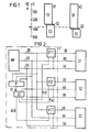
- Fig. 1 eine Darstellung von möglichen Speichervarianten und
- Fig. 2 ein Blockschaltbild der Schaltungsanordnung.
- Fig. 1 shows a representation of possible memory variants and
- Fig. 2 is a block diagram of the circuit arrangement.
Bei der Darstellung in Fig.1 wird angenommen, daß an dem Mikrorechnersystem drei Speichereinheiten S1 bis S3 angeschlossen sind, die für den Mikroprozessor einen Adressenbereich von 64 K bilden. Die Speichereinheit S1 ist beispielsweise als Festwertspeicher ausgebildet und hat einen Speicherbereich von 47 K. Die Speichereinheit S2 ist als elektrisch änderbarer Festwertspeicher ausgebildet und hat einen Adressenbereich von 1 K. Die Speichereinheit S3 schließlich ist als Schreib-Lese-Speicher ausgebildet und hat einen Adressenbereich von 23 K.1 it is assumed that three memory units S1 to S3 are connected to the microcomputer system, which form an address range of 64 K for the microprocessor. The memory unit S1 is designed, for example, as a read-only memory and has a memory area of 47 K. The memory unit S2 is designed as an electrically changeable read-only memory and has an address range of 1 K. Finally, the storage unit S3 is designed as a read-write memory and has an address range of 23 K.
Für eine erste Systemvariante V1 wird angenommen, daß der Adressenbereich der Speichereinheit S1 bei der Adresse AD = 0, der Adressenbereich des der Speichereinheit S2 bei der Adresse AD = 40 K und der Adressenbereich der Speichereinheit S3 bei der Adresse AD = 41 K beginnt. Für eine zweite Systemvariante V2 wird angenommen, daß der Adressenbereich der Speichereinheit S1 ebenfalls bei der Adresse AD = 0 beginnt, der Adressenbereich der Speichereinheit S2 jedoch bei der Adresse AD = 47 K und der Adressenbereich der Speichereinheit S3 bei der Adresse AD = 48 K beginnt.For a first system variant V1, it is assumed that the address area of the storage unit S1 begins at the address AD = 0, the address area of the storage unit S2 at the address AD = 40 K and the address area of the storage unit S3 at the address AD = 41 K. For a second system variant V2, it is assumed that the address area of the storage unit S1 also begins at the address AD = 0, but the address area of the storage unit S2 begins at the address AD = 47 K and the address area of the storage unit S3 at the address AD = 48 K .
Wenn die Systemvarianten V1 und V2, gesteuert durch das dem Mikrorechner zugeordnete Programm, beliebig umschaltbar sein sollen, müssen die Speichereinheiten S1 bis S3 die angegebenen Adressenbereiche aufweisen. Falls jedoch für ein bestimmtes Gerät das Programm nicht beliebig änderbar ist und in einem Festwertspeicher gespeichert ist und damit festliegt, welche Systemvariante oder welche Systemvarianten eingestellt werden könnten, müssen die entsprechenden Speicherbaugruppen selbstverständlich nur so weit mit Speicherbausteinen bestückt werden, wie es für die entsprechenden Systemvarianten erforderlich ist. Wird nun der Gesamtspeicher beispielsweise durch einen bei der durch einen Pfeil gekennzeichneten Stelle AD = 45 K adressiert, so werden sowohl in der Speichereinheit S1 als auch in der Speichereinheit S3 entsprechende Speicherbereiche adressiert. Zum Unterscheiden der beiden Systemvarianten V1 und V2 ist bei der Schaltungsanordnung ein entsprechender Decodierer vorgesehen, dem einerseits die höchstwertigen Adressbits der Adresse AD und dem andererseits Steuersignale zugeführt werden, die von einem am Mikroprozessor angeschlossenen Ausgabebaustein abgegebenwerden und die die entsprechende Systemvariante festlegen. Der Decodierer gibt Auswahlsignale ab, die die Daten auf nur jeweils einem den Speichereinheiten S1 bis S3 zugeordneten Datenbus freigeben.If the system variants V1 and V2, controlled by the program assigned to the microcomputer, are to be switchable as desired, the memory units S1 to S3 must have the specified address ranges. However, if the program cannot be changed arbitrarily for a particular device and is stored in a read-only memory and thus it is determined which system variant or which system variants could be set, the corresponding memory modules need of course only be equipped with memory modules to the extent that it is for the corresponding system variants is required. If the total memory is now addressed, for example, by an AD = 45 K at the location indicated by an arrow, corresponding memory areas are addressed both in the memory unit S1 and in the memory unit S3. To distinguish between the two system variants V1 and V2, a corresponding decoder is provided in the circuit arrangement, on the one hand the most significant address bits the address AD and, on the other hand, control signals are supplied which are emitted by an output module connected to the microprocessor and which determine the corresponding system variant. The decoder emits selection signals which release the data on only one data bus assigned to the memory units S1 to S3.
Bei der in Fig.2 dargestellten Schaltungsanordnung ist ein Zentralsystem Z vorgesehen, das einen Mikroprozessor MP enthält, der in bekannter Weise mit einem Datenbus DB, einem Adressbus AB und einem Steuerbus SB versehen ist. An dem Zentralsystem sind die drei Speichereinheiten S1 bis S3 jeweils über den Datenbus DB, den Adressbus AB und den Steuerbus SB angeschlossen. Die Speichereinheiten S1 bis S3 sind beispielsweise aus integrierten Speicherbausteinen aufgebaut, die unter der Bezeichnung 2732, ER 3400 bzw. MK 4104 im Handel erhältlich sind.In the circuit arrangement shown in FIG. 2, a central system Z is provided which contains a microprocessor MP which is provided in a known manner with a data bus DB, an address bus AB and a control bus SB. The three memory units S1 to S3 are each connected to the central system via the data bus DB, the address bus AB and the control bus SB. The memory units S1 to S3 are constructed, for example, from integrated memory modules which are commercially available under the designation 2732, ER 3400 or MK 4104.
An den Mikroprozessor MP ist in bekannter Weise ein Ausgabebaustein (Port-Baustein) P angeschlossen der unter der Bezeichnung 8255 A im Handel erhältlich ist. Diesem Ausgabe-Baustein P ist der Decodierer DC nachgeschaltet, der eingangsseitig zusätzlich mit dem Adressbus AB und dem Steuerbus SB verbunden ist, erzeugt Auswahlsignale A1 bis A3, die der Auswahl der entsprechenden Speichereinheit S1 bis S3 dienen und die den bidirektionalen Bustreibern BT1 bis BT3 zugeführt werden, die jeweils im Verbindungsweg zwischen dem Mikroprozessor MP und einer der Speichereinheiten S1 bis S3 angeordnet sind. Der Decodierer DC ist vorzugsweise als Festwertspeicher, beispielsweise als programmierbarer Festwertspeicher, ausgebildet.An output module (port module) P, which is commercially available under the designation 8255 A, is connected to the microprocessor MP in a known manner. This output module P is followed by the decoder DC, which is additionally connected on the input side to the address bus AB and the control bus SB, and generates selection signals A1 to A3, which are used to select the corresponding memory unit S1 to S3 and which are supplied to the bidirectional bus drivers BT1 to BT3 are arranged in the connection path between the microprocessor MP and one of the storage units S1 to S3. The decoder DC is preferably designed as a read-only memory, for example as a programmable read-only memory.
Zum Einstellen der Systemvariante V1 liest der Mikroprozessor MP aus der Speichereinheit Slin bekannter Weise entsprechende Befehle aus, um den Ausgabebaustein P entsprechend anzusteuern, so daß die von ihm abgegebenen Steuersignale ST der Systemvariante V1 zugeordnete Binärwerte annehmen. Wenn, entsprechend Fig.1, der Mikroprozessor MP auf den Adressbus AB die Adresse AD = 45 K gibt, wird diese Adresse allen Speichereinheiten S1 bis S3 zugeführt. Über den Steuerbus SB werden, beispielsweise zur Durchführung eines Lesevorgangs, entsprechende Steuersignale abgegeben. Aus allen Steuereinheiten S1 bis S3 werden nun die entsprechenden Daten ausgelesen und auf den Datenbus DB gegeben. Die Daten werden jedoch nur von dem Bustreiber BT3 freigegeben und zum Mikroprozessor MP durchgeschaltet. Die Freigabe erfolgt durch das vom Decodierer DC abgegebene Auswahlsignal A3, das in Abhängigkeit von den höchstwertigen Bits der Adresse AD und den Binärwerten der Steuersignale ST erzeugt wird.In order to set the system variant V1, the microprocessor MP reads out appropriate commands from the memory unit Slin in a known manner in order to control the output module P accordingly, so that the control signals ST it issues assume binary values assigned to the system variant V1. If, according to FIG. 1, the microprocessor MP gives the address AD = 45 K on the address bus AB, this address is supplied to all memory units S1 to S3. Corresponding control signals are emitted via the control bus SB, for example to carry out a read operation. The corresponding data are now read out from all control units S1 to S3 and transferred to the data bus DB. However, the data is only released by the bus driver BT3 and switched through to the microprocessor MP. The release takes place through the selection signal A3 emitted by the decoder DC, which is generated as a function of the most significant bits of the address AD and the binary values of the control signals ST.
In entsprechender Weise wird, wenn über den Ausgabebaustein P die Systemvariante V2 eingestellt wurde, vom Decodierer DC ein Auswahlsignal A1 an den Bustreiber BT1 abgegeben und nur die von der Speichereinheit S1 abgegebenen Daten werden über den Datenbus DB zum Mikroprozessor MP durchgeschaltet. Die übrigen Bustreiber BT2 und BT3 sind dann gesperrt.In a corresponding manner, if the system variant V2 has been set via the output module P, the decoder DC outputs a selection signal A1 to the bus driver BT1 and only the data output by the memory unit S1 is connected through the data bus DB to the microprocessor MP. The other bus drivers BT2 and BT3 are then blocked.
Die Anzahl der höchstwertigen Bits der Adresse AD, die dem Decodierer DC zugeführt werden, hängt von dem Verhältnis des Adressenbereichs der kleinsten Speichereinheit zum Adressenbereich des Gesamtspeichers ab. Wenn, wie bei dem in Fig.1 dargestellten Beispiel, die Speichereinheit S2 nur einen Adressenbereich von 1 K aufweist, und der Adressenbereich des Gesamtspeichers 64 K beträgt, sind 64 derartige kleinste Speichereinheiten adressierbar, so daß dem Decodierer DC die Adressbits 10 bis 15, also 6 Adressbits,zugeführt werden müssen.The number of the most significant bits of the address AD, which are supplied to the decoder DC, depends on the ratio of the address area of the smallest memory unit to the address area of the total memory. If, as in the example shown in FIG. 1, the memory unit S2 has only an address area of 1 K and the address area of the total memory is 64 K, 64 such smallest memory units are addressable, so that the address bits 10 to 15, ie 6 address bits, must be supplied to the decoder DC.
Falls in einer der Speichereinheiten S1 bis S3 Daten eingeschrieben werden sollen, erfolgt das Durchschalten der Daten zu den Speichereinheiten S1 bis S3 ebenfalls in Abhängigkeit von den Auswahlsignalen A1 bis A3. Falls die Speichereinheit S1 jedoch als Festwertspeicher ausgebildet ist, ist es selbstverständlich nicht möglich, in diesem Speicher Daten über den Datenbus DB einzuschreiben. Falls mehrere Speichereinheiten die gleichen Adressen aufweisen, kann der Decodierer DC auch die Funktion übernehmen, die Speicherinhalte von nicht ausgewählten Speichereinheiten vor einem schreibenden Zugriff zu schützen, indem er beispielsweise auf dem Steuerbus SB entsprechende Signale erzeugt.If data are to be written into one of the memory units S1 to S3, the switching through of the data to the memory units S1 to S3 also takes place as a function of the selection signals A1 to A3. However, if the memory unit S1 is designed as a read-only memory, it is of course not possible to write data into this memory via the data bus DB. If several memory units have the same addresses, the decoder DC can also take over the function of protecting the memory contents of non-selected memory units from write access, for example by generating corresponding signals on the control bus SB.
Claims (4)
dadurch gekennzeichnet, daß ein Decodierer (DC) vorgesehen ist, der eingangsseitig
mit dem Adressbus (AB) und mit den Ausgängen eines am Mikroprozessor (MP) angeschlossenen Ausgabebausteins (P) verbunden ist, und der in Abhängigkeit von vom Ausgabebaustein (P) abgegebenen Steuersignalen (ST) und von den höchstwertigen Bits der am Adressenbus (AB) jeweils anliegenden Adresse (AD) den Speichereinheiten (S1 bis S3) vorgeschaltete Bustreiber (BT1 bis BT3) freigibt oder sperrt.1. Circuit arrangement for addressing different memory units in a microcomputer system, in which the memory units are connected to a central system via a data bus, an address bus and a control bus,
characterized in that a decoder (DC) is provided on the input side
is connected to the address bus (AB) and to the outputs of an output module (P) connected to the microprocessor (MP), and depending on the control signals (ST) emitted by the output module (P) and the most significant bits of those on the address bus (AB) each available address (AD) the bus units (S1 to S3) upstream bus drivers (BT1 to BT3) enables or blocks.
Applications Claiming Priority (2)
| Application Number | Priority Date | Filing Date | Title |
|---|---|---|---|
| DE3148761 | 1981-12-09 | ||
| DE19813148761 DE3148761C2 (en) | 1981-12-09 | 1981-12-09 | Circuit arrangement for addressing different memory units in a microcomputer system |
Publications (2)
| Publication Number | Publication Date |
|---|---|
| EP0081224A2 true EP0081224A2 (en) | 1983-06-15 |
| EP0081224A3 EP0081224A3 (en) | 1986-02-05 |
Family
ID=6148288
Family Applications (1)
| Application Number | Title | Priority Date | Filing Date |
|---|---|---|---|
| EP82111269A Withdrawn EP0081224A3 (en) | 1981-12-09 | 1982-12-06 | Circuit arrangement for the addressing of different memory units in a micro computer system |
Country Status (2)
| Country | Link |
|---|---|
| EP (1) | EP0081224A3 (en) |
| DE (1) | DE3148761C2 (en) |
Cited By (1)
| Publication number | Priority date | Publication date | Assignee | Title |
|---|---|---|---|---|
| GB2190771A (en) * | 1986-05-23 | 1987-11-25 | Mitsubishi Electric Corp | Memory device |
Families Citing this family (1)
| Publication number | Priority date | Publication date | Assignee | Title |
|---|---|---|---|---|
| US4979148A (en) * | 1988-12-09 | 1990-12-18 | International Business Machines Corporation | Increasing options in mapping ROM in computer memory space |
Citations (2)
| Publication number | Priority date | Publication date | Assignee | Title |
|---|---|---|---|---|
| US4296467A (en) * | 1978-07-03 | 1981-10-20 | Honeywell Information Systems Inc. | Rotating chip selection technique and apparatus |
| DE3102210A1 (en) * | 1981-01-23 | 1982-08-19 | Siemens AG, 1000 Berlin und 8000 München | Circuit arrangement for selecting memory areas |
-
1981
- 1981-12-09 DE DE19813148761 patent/DE3148761C2/en not_active Expired
-
1982
- 1982-12-06 EP EP82111269A patent/EP0081224A3/en not_active Withdrawn
Patent Citations (2)
| Publication number | Priority date | Publication date | Assignee | Title |
|---|---|---|---|---|
| US4296467A (en) * | 1978-07-03 | 1981-10-20 | Honeywell Information Systems Inc. | Rotating chip selection technique and apparatus |
| DE3102210A1 (en) * | 1981-01-23 | 1982-08-19 | Siemens AG, 1000 Berlin und 8000 München | Circuit arrangement for selecting memory areas |
Non-Patent Citations (2)
| Title |
|---|
| ELECTRONICS, Band 48, Nr. 24, 27. November 1975, Seiten 105-107, New York, US;J.A. KUZDRALL:"Memory, peripherals share microprocessor address range" * |
| IBM TECHNICAL DISCLOSURE BULLETIN, Band 18, Nr. 7, Dezember 1975, Seiten 2231-2232, New York, US; G.H. FOSTER et al.: "Functional memory holding data base like structures * |
Cited By (2)
| Publication number | Priority date | Publication date | Assignee | Title |
|---|---|---|---|---|
| GB2190771A (en) * | 1986-05-23 | 1987-11-25 | Mitsubishi Electric Corp | Memory device |
| GB2190771B (en) * | 1986-05-23 | 1990-08-22 | Mitsubishi Electric Corp | Memory device |
Also Published As
| Publication number | Publication date |
|---|---|
| DE3148761A1 (en) | 1983-06-16 |
| EP0081224A3 (en) | 1986-02-05 |
| DE3148761C2 (en) | 1985-08-22 |
Similar Documents
| Publication | Publication Date | Title |
|---|---|---|
| DE3906497A1 (en) | SELF-CONFIGURING STORAGE SYSTEM | |
| DE3835297C2 (en) | Data processing system with an address bus control device | |
| DE2364254B2 (en) | CIRCUIT ARRANGEMENT FOR DATA PROCESSING DEVICES | |
| DE2926322C2 (en) | Storage subsystem | |
| DE2952500C2 (en) | ||
| DE2758829A1 (en) | MULTIPROCESSOR DATA PROCESSING SYSTEM | |
| DE2718551B2 (en) | ||
| DE2846054C2 (en) | Circuit arrangement for expanding the addressing volume of a central unit, in particular a microprocessor | |
| DE2648225C2 (en) | Data storage device | |
| DE3024153A1 (en) | STORAGE SUBSYSTEM | |
| DE3148761C2 (en) | Circuit arrangement for addressing different memory units in a microcomputer system | |
| DE4026581C2 (en) | ||
| DE2235883C3 (en) | Data processing device | |
| DE3149926A1 (en) | Programmable comparison circuit | |
| DE2233164A1 (en) | CIRCUIT ARRANGEMENT FOR HIDING ANY SELECTABLE AREA OF A BIT SEQUENCE WHEN TRANSFERRED BETWEEN TWO REGISTERS | |
| DE4223532A1 (en) | Circuit arrangement for checking the addressing of at least one matrix | |
| CH616752A5 (en) | ||
| DE4124414C2 (en) | Interruption order | |
| DE3009121B1 (en) | Micro program control device | |
| DE2327375C2 (en) | PCM exchange with time division and space division facilities | |
| DE3417816A1 (en) | Programmable switching network | |
| DE3116471C2 (en) | ||
| DE2907835C2 (en) | Address multiplexer for a main memory | |
| DE3009329C2 (en) | Hybrid associative memory | |
| EP0262608A1 (en) | Arrangement for priority selection in an interrupt controller |
Legal Events
| Date | Code | Title | Description |
|---|---|---|---|
| PUAI | Public reference made under article 153(3) epc to a published international application that has entered the european phase |
Free format text: ORIGINAL CODE: 0009012 |
|
| AK | Designated contracting states |
Designated state(s): CH FR GB IT LI SE |
|
| 17P | Request for examination filed |
Effective date: 19841217 |
|
| PUAL | Search report despatched |
Free format text: ORIGINAL CODE: 0009013 |
|
| AK | Designated contracting states |
Designated state(s): CH FR GB IT LI SE |
|
| 17Q | First examination report despatched |
Effective date: 19870130 |
|
| R17C | First examination report despatched (corrected) |
Effective date: 19870626 |
|
| STAA | Information on the status of an ep patent application or granted ep patent |
Free format text: STATUS: THE APPLICATION IS DEEMED TO BE WITHDRAWN |
|
| 18D | Application deemed to be withdrawn |
Effective date: 19880702 |
|
| RIN1 | Information on inventor provided before grant (corrected) |
Inventor name: FUECHSLE, WILLY, ING. GRAD. |