EP0079651B1 - Photo-electric detection structure - Google Patents
Photo-electric detection structure Download PDFInfo
- Publication number
- EP0079651B1 EP0079651B1 EP82201421A EP82201421A EP0079651B1 EP 0079651 B1 EP0079651 B1 EP 0079651B1 EP 82201421 A EP82201421 A EP 82201421A EP 82201421 A EP82201421 A EP 82201421A EP 0079651 B1 EP0079651 B1 EP 0079651B1
- Authority
- EP
- European Patent Office
- Prior art keywords
- photo
- substrate
- radiations
- detection structure
- glass
- Prior art date
- Legal status (The legal status is an assumption and is not a legal conclusion. Google has not performed a legal analysis and makes no representation as to the accuracy of the status listed.)
- Expired
Links
Images

Classifications
-
- G—PHYSICS
- G01—MEASURING; TESTING
- G01T—MEASUREMENT OF NUCLEAR OR X-RADIATION
- G01T1/00—Measuring X-radiation, gamma radiation, corpuscular radiation, or cosmic radiation
- G01T1/16—Measuring radiation intensity
- G01T1/20—Measuring radiation intensity with scintillation detectors
- G01T1/2002—Optical details, e.g. reflecting or diffusing layers
-
- H—ELECTRICITY
- H01—ELECTRIC ELEMENTS
- H01J—ELECTRIC DISCHARGE TUBES OR DISCHARGE LAMPS
- H01J29/00—Details of cathode-ray tubes or of electron-beam tubes of the types covered by group H01J31/00
- H01J29/02—Electrodes; Screens; Mounting, supporting, spacing or insulating thereof
- H01J29/10—Screens on or from which an image or pattern is formed, picked up, converted or stored
- H01J29/36—Photoelectric screens; Charge-storage screens
- H01J29/38—Photoelectric screens; Charge-storage screens not using charge storage, e.g. photo-emissive screen, extended cathode
Definitions
- the present invention relates to a photoelectric detection structure consisting of a photoemissive layer based on alkali metals deposited on a substrate made of a material transparent to radiation of visible light and near infrared and in the form of a plate with flat, convex or concaves of limited curvature so that the incidence of rays in parallel beams does not exceed 15 to 20 °, the substrate being provided on the radiation incidence face with means for attenuating the reflection of the radiation on this face.
- the thickness of the photoemissive layer is dimensioned so that, taking into account the nature of its constituent material, the nature of the substrate and said optical means, the photoelectric yield of the structure is optimized for a certain spectral range of incident radiation.
- An application of the present invention is in particular a detection structure usable in radiography.
- the invention is found to be in close relation with the devices including at the input such a photoelectric detection structure, such as the photoelectric cells, the image intensifier tubes, the tubes integrated into the pickup systems. view of television or photomultipliers.
- a photoelectric detection structure such as the photoelectric cells, the image intensifier tubes, the tubes integrated into the pickup systems. view of television or photomultipliers.
- the photoelectric detection structure used comprises a photoemissive layer deposited directly on the substrate, this generally results in poor optical adaptation of the photoemissive layer on the substrate, so that a good part of the light incident on the substrate is badly used for the conversion of photons into electrons and that the photoelectric detection efficiency of said structure is considerably reduced.
- the prior art reported for example in United States Patent No. 3,254,253, has provided for improving this efficiency by attenuating the phenomena of reflection which occur at the substrate / photoemissive layer interface by means of at least one intermediate layer transparent to incident radiation, placed between substrate and photoemissive layer and whose refractive index is between those of said substrate and photoemissive layer, respectively of the order of 1.5 and 3.
- the thickness of the layer intermediate must be adjusted so that, taking into account the optical constants of the substrate and photoemissive layer materials, the lights reflected respectively at the substrate / intermediate layer interface and at the intermediate layer / photoemissive layer interface, are substantially of equal amplitude and opposite phases, so that they tend to cancel each other out by interference.
- the structure is especially suitable for detection with image transport thanks to the optical fibers which it comprises and it is much less suitable, because of said fibers, for detection of phenomena in volume without image formation. .
- the higher index of the fiber core glass with respect to air this results in poor optical adaptation of the structure at the level of the entry face of the structure.
- document GB A 2 051 348 describes a detector with a scintillator in front of the glass substrate.
- the intermediate layers of variable indices are interposed, these can only transmit part of the light flux.
- This document only concerns the scintillator-glass substrate interface and does not examine the glass substrate-photocathode interface or the mechanisms of electron emission by the photocathode, i.e. the photoelectric efficiency of the detector assembly.
- the object of the invention is to propose a photoelectric detection structure of construction which is easier to produce, due to the absence of an intermediate layer between the substrate and the photoemissive layer, without the photoelectric efficiency being significantly different.
- Another object of the invention is also that this structure is suitable for volume detection of photonic phenomena.
- the invention proposes to use as a photoemissive layer substrate a massive plate of transparent material with a refractive index of the order of 2.
- a massive plate of transparent material with a refractive index of the order of 2.
- means attenuating the reflection of radiation on this face are in particular an anti-reflection layer of the known art.
- the structure is remarkable in that the refractive index of the substrate material for said radiation is close to 2, the substrate material being chosen from the following glasses: lanthanum glass, barium glass , titanium glass, the photoemissive layer being an alkaline layer of chemical formula Sb K 2 Cs, or Sb Rb 2 Cs or Sb Cs 3 .
- the structure is remarkable in that the refractive index of the substrate material for said radiation is close to 2, the substrate material being chosen from the following glasses: lanthanum glass, glass with barium, titanium glass, the photoemissive layer being tri-alkaline with chemical formula (Sb Na 2 K, Cs).
- the structure is remarkable in that the means for attenuating the reflection of the radiation incident on the substrate consist of a scintillator crystal plate pressed against the substrate, said crystal having a refractive index of light. close to 1.8, like a crystal of chemical formula (Csl, Na), (Csl, TI).
- the high index of this crystal close to that of the substrate, allows the desired optical adaptation.
- the invention then consists of a detection structure which can be used for example in radiography or X-ray spectrometry.
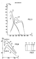
- FIG. 1 represents the structure according to the invention comprising the substrate consisting of a plate 11 transparent to radiation of visible and near infrared light, the photoemissive layer 12 of thickness "e" and the anti-reflection layer 13 on the face of substrate opposite to the photoemissive layer.
- the faces of the plate 11 are assumed to be plane and parallel.
- the invention extends to the case where said faces are concave or convex insofar as their curvatures are limited so that the incidence of rays of light in parallel beam does not exceed 15 to 20 °.
- This structure is supposed to constitute the entry of a photoelectric tube, the light to be detected being present on the left side of the stack in the direction of arrow 14, the vacuum 15 of the tube being on the right side.
- the substrate is made of a material transparent to visible and near infrared light among those with the highest refractive indices of around 2, a lanthanum glass for example, to be compared to that of around 3 photoemissive materials.
- the mission of the anti-reflection layer 13 is to optically adapt this substrate on the outside of the tube, which is placed for example in air, therefore in a medium with a refractive index of the order of 1, so minimize radiation reflection at the substrate / exterior interface of the tube as much as possible.
- the photoemissive layer 12 consists of a tri-alkaline material of chemical formula Sb Na 2 K Cs, of the type of those constituting a layer S 20 or S 25.
- the substrate is a glass of high refractive index, a lanthanum glass for example of index 1.9 and the anti-reflection layer is of the known art, for example a layer of a material such as Mg F 2 , Na 3 AI F 6 , Ca F 2 , Sr F 2 , Sa F 2 , AI F 3 , (Mg F 2 , Ce F 3 ), Th F 4 .
- a material such as Mg F 2 , Na 3 AI F 6 , Ca F 2 , Sr F 2 , Sa F 2 , AI F 3 , (Mg F 2 , Ce F 3 ), Th F 4 .
- the curves representative of the efficiency, for each of these wavelengths, are respectively the curves in solid lines 24, 25, 26.
- FIG. 3 indicates respectively, for a layer S 20 and a layer S 25, the spectral sensitivity of structure according to this first embodiment compared to the spectral sensitivity of structure of the prior art comprising respectively the same layer S 20 and the same layer S 25, deposited on ordinary glass.
- the curves relating to the invention are the curves in solid lines 31 and 32 for the layers S 20 and S 25 respectively.
- the curves relating to the prior art are the curves in broken lines respectively 33 and 34.
- the photoemissive layer 12 is bi-alkaline of type Sb K 2 Cs, Sb Rb 2 Cs or mono-alkaline Sb Cs 3
- the substrate 11 is still a glass of high refractive index, glass with lanthanum for example, of index 1.9; the anti-reflection layer 13 being of the known art.
- the curves representative of the photoelectric efficiency p;, as a function of the thickness of the layer are respectively 41, 42 for the structure according to the invention, and 43, 44 for the known art.
- FIG. 5 represents a third embodiment of the invention.
- the structure is provided, on the entry face side of the substrate, with a light scintillator crystal 61 under the action, for example, of X or gamma rays.
- This crystal 61 can have the shape of a blade with parallel faces.
- the crystal as well as the entry face of the photocathode substrate can in fact have very diverse shapes: plane, spherical, concave, convex ...
- Its constituent material has a high refractive index of the order of 1.8, as for example that of chemical formula (Csl, Na), (Csl, TI).
- the structure thus benefits from good optical adaptation to the scintillator / photocathode substrate interface without the use of anti-reflection layers as in the previous embodiments of the invention.
Description
La présente invention concerne une structure de détection photoélectrique constituée d'une couche photoémissive à base de métaux alcalins déposée sur un substrat constitué en un matériau transparent aux radiations de la lumière visible et du proche infrarouge et en forme de plaque à faces planes, convexes ou concaves de courbures limitées de telle sorte que l'incidence des rayons en faisceaux parallèles n'excède pas 15 à 20°, le substrat étant muni, sur la face d'incidence des radiations, de moyens d'atténuation de la réflexion des radiations sur cette face. L'épaisseur de la couche photoémissive est dimensionnée pour que, compte-tenu de la nature de son matériau constitutif, de la nature du substrat et desdits moyens optiques, le rendement photoélectrique de la structure soit optimalisé pour un certain domaine spectral des radiations incidentes.The present invention relates to a photoelectric detection structure consisting of a photoemissive layer based on alkali metals deposited on a substrate made of a material transparent to radiation of visible light and near infrared and in the form of a plate with flat, convex or concaves of limited curvature so that the incidence of rays in parallel beams does not exceed 15 to 20 °, the substrate being provided on the radiation incidence face with means for attenuating the reflection of the radiation on this face. The thickness of the photoemissive layer is dimensioned so that, taking into account the nature of its constituent material, the nature of the substrate and said optical means, the photoelectric yield of the structure is optimized for a certain spectral range of incident radiation.
Une application de la présente invention est en particulier une structure de détection utilisable en gammagraphie. D'une façon générale, l'invention se trouve être en rapport étroit avec les dispositifs incluant à l'entrée une telle structure de détection photoélectrique, tels les cellules photoélectriques, les tubes intensificateurs d'image, les tubes intégrés aux systèmes de prise de vue de télévision ou encore les photomultiplicateurs. Dans ces dispositifs, lorsque la structure de détection photoélectrique utilisée comporte une couche photoémissive déposée directement sur le substrat, il s'ensuit généralement une mauvaise adaptation optique de la couche photoémissive sur le substrat, si bien qu'une bonne partie de la lumière incidente sur le substrat est mal utilisée pour la conversion des photons en électrons et que l'efficacité de détection photoélectrique de ladite stucture se trouve considérablement réduite.An application of the present invention is in particular a detection structure usable in radiography. In general, the invention is found to be in close relation with the devices including at the input such a photoelectric detection structure, such as the photoelectric cells, the image intensifier tubes, the tubes integrated into the pickup systems. view of television or photomultipliers. In these devices, when the photoelectric detection structure used comprises a photoemissive layer deposited directly on the substrate, this generally results in poor optical adaptation of the photoemissive layer on the substrate, so that a good part of the light incident on the substrate is badly used for the conversion of photons into electrons and that the photoelectric detection efficiency of said structure is considerably reduced.
L'art antérieur, signalé par exemple dans le brevet des Etats-Unis n° 3 254 253, à prévu d'améliorer cette efficacité en atténuant les phénomènes de réflexion qui se produisent à l'interface substrat/couche photoémissive au moyen d'au moins une couche intermédiaire transparente aux radiations incidentes, placée entre substrat et couche photoémissive et dont l'indice de réfraction est compris entre ceux desdits substrat et couche photoémissive, respectivement de l'ordre de 1,5 et 3. L'épaisseur de la couche intermédiaire doit être ajustée pour que, compte-tenu des constantes optiques des matériaux de substrat et de couche photoémissive, les lumières réfléchies respectivement à l'interface substrat/couche intermédiaire et à l'interface couche intermédiaire/couche photoémissive, soient sensiblement de même amplitude et de phases opposées, si bien qu'elles tendent à s'annuler mutuellement par interférence. L'élaboration de cette couche intermédiaire avec une épaisseur mesurée avec précision rend délicate la construction de la structure. Pour minimiser les pertes par réflexion à l'interface substrat/couche photoémissive, on peut penser à choisir un substrat d'indice de réfraction plus élevé que celui du verre ordinaire. C'est ce qui est réalisé, du moins partiellement, comme décrit dans "Actualités R.T.C." n 41, avril 1978, p. 22 - 23, lorsque la couche photoémissive est déposée sur la section d'un faisceau de fibres conductrices de la lumière et dont le verre de coeur est un verre au lanthane d'indice 1,9. Mais, le dispositif présente alors deux sortes d'inconvénients. D'une part, la structure est surtout adaptée à une détection avec transport d'image grâce aux fibres optiques qu'elle comporte et elle est beaucoup moins apte, à cause desdites fibres, à une détection de phénomènes en volume sans formation d'image. D'autre part, du fait du plus fort indice du verre de coeur de fibre par rapport à l'air, il en résulte une mauvaise adaptation optique de la structure au niveau de la face d'entrée de la structure.The prior art, reported for example in United States Patent No. 3,254,253, has provided for improving this efficiency by attenuating the phenomena of reflection which occur at the substrate / photoemissive layer interface by means of at least one intermediate layer transparent to incident radiation, placed between substrate and photoemissive layer and whose refractive index is between those of said substrate and photoemissive layer, respectively of the order of 1.5 and 3. The thickness of the layer intermediate must be adjusted so that, taking into account the optical constants of the substrate and photoemissive layer materials, the lights reflected respectively at the substrate / intermediate layer interface and at the intermediate layer / photoemissive layer interface, are substantially of equal amplitude and opposite phases, so that they tend to cancel each other out by interference. The development of this intermediate layer with a thickness measured with precision makes the construction of the structure difficult. To minimize the losses by reflection at the substrate / photoemissive layer interface, one can think of choosing a substrate with a higher refractive index than that of ordinary glass. This is what is achieved, at least partially, as described in "Actualités R.T.C."
D'autre part le document GB A 2 051 348 décrit un détecteur avec un scintillateur devant le substrat de verre. Pour assurer le transfert du rayonnement émis par le scintillateur vers la face d'entrée du photomultiplicateur des couches intermédiaires d'indices variables sont interposées celles-ci ne peuvent transmettre qu'une partie du flux lumineux. Ce document ne concerne que l'interface scintillateur-substrat de verre et n'examine pas l'interface substrat de verre-photocathode ni les mécanismes d'émission d'électrons par la photocathode c'est-à-dire le rendement photoélectrique de l'ensemble du détecteur.On the other hand, document GB A 2 051 348 describes a detector with a scintillator in front of the glass substrate. To ensure the transfer of the radiation emitted by the scintillator towards the input face of the photomultiplier, the intermediate layers of variable indices are interposed, these can only transmit part of the light flux. This document only concerns the scintillator-glass substrate interface and does not examine the glass substrate-photocathode interface or the mechanisms of electron emission by the photocathode, i.e. the photoelectric efficiency of the detector assembly.
Le but de l'invention est de proposer une structure de détection photoélectrique de construction plus facile à réaliser, du fait de l'inexistence de couche intermédiaire entre substrat et couche photoémissive, sans que le rendement photoélectrique soit sensiblement différent. Un autre but de l'invention est encore que cette structure soit apte à une détection en volume de phénomènes photoniques. Pour cela, l'invention propose d'utiliser comme substrat de couche photoémissive une plaque massive en matériau transparent d'indice de réfraction de l'ordre de 2. De plus, pour éviter une mauvaise adaptation de la structure du côté face d'entrée, celle-ci est munie de moyens atténuant la réflexion de radiations sur cette face. Ces moyens sont en particulier une couche anti-reflet de l'art connu.The object of the invention is to propose a photoelectric detection structure of construction which is easier to produce, due to the absence of an intermediate layer between the substrate and the photoemissive layer, without the photoelectric efficiency being significantly different. Another object of the invention is also that this structure is suitable for volume detection of photonic phenomena. For this, the invention proposes to use as a photoemissive layer substrate a massive plate of transparent material with a refractive index of the order of 2. In addition, to avoid poor adaptation of the structure on the input face side , it is provided with means attenuating the reflection of radiation on this face. These means are in particular an anti-reflection layer of the known art.
Selon une variante de l'invention, la structure est remarquable en ce que l'indice de réfraction du matériau du substrat pour lesdites radiations est voisin de 2, le matériau de substrat étant choisi parmi les verres suivants: verre au lanthane, verre au baryum, verre au titane, la couche photoémissive étant une couche alcaline de formule chimique Sb K2 Cs, ou Sb Rb2 Cs ou Sb Cs3.According to a variant of the invention, the structure is remarkable in that the refractive index of the substrate material for said radiation is close to 2, the substrate material being chosen from the following glasses: lanthanum glass, barium glass , titanium glass, the photoemissive layer being an alkaline layer of chemical formula Sb K 2 Cs, or Sb Rb 2 Cs or Sb Cs 3 .
Selon une autre variante de l'invention, la structure est remarquable en ce que la l'indice de réfraction du matériau de substrat pour lesdites radiations est voisin de 2, le matériau de substrat étant choisi parmi les verres suivants: verre au lanthane, verre au baryum, verre au titane, la couche photoémissive étant tri-alcaline de formule chimique (Sb Na2K, Cs).According to another variant of the invention, the structure is remarkable in that the refractive index of the substrate material for said radiation is close to 2, the substrate material being chosen from the following glasses: lanthanum glass, glass with barium, titanium glass, the photoemissive layer being tri-alkaline with chemical formula (Sb Na 2 K, Cs).
Selon une autre variante, la structure est remarquable en ce que les moyens d'atténuation de la réflexion des radiations incidentes sur le substrat sont constitués d'une lame de cristal scintillateur plaquée contre le substrat, ledit cristal présentant un indice de réfraction de la lumière voisin de 1,8, tel un cristal de formule chimique (Csl, Na), (Csl, TI). L'indice élevé de ce cristal, proche de celui du substrat, permet l'adaptation optique désirée. L'invention consiste alors en une structure de détection utilisable par exemple en gammagraphie ou en spectrométrie de photons X.According to another variant, the structure is remarkable in that the means for attenuating the reflection of the radiation incident on the substrate consist of a scintillator crystal plate pressed against the substrate, said crystal having a refractive index of light. close to 1.8, like a crystal of chemical formula (Csl, Na), (Csl, TI). The high index of this crystal, close to that of the substrate, allows the desired optical adaptation. The invention then consists of a detection structure which can be used for example in radiography or X-ray spectrometry.
L'invention apparaît sous plusieurs de ses modes de réalisation donnés à titre d'exemples, non limitatifs, dans la description suivante, celle-ci étant accompagnée de dessins qui représentent:
- Figure 1: une vue schématique de la structure photoélectrique selon l'invention;
- Figure 2: des courbes donnant le rendement photoélectrique en fonction de l'épaisseur de la couche photoémissive d'une structure de détection photoélectrique selon un premier mode de réalisation de l'invention, la couche photoémissive étant tri-alcaline de formule (Sb Na2 K Cs), comparé au rendement de la même couche photoémissive déposée sur un verre ordinaire;
- Figure 3: des courbes donnant la sensibilité spectrale de la structure selon le premier mode de réalisation munie d'une
couche S 20 ouS 25 et celles des mêmes couches déposées sur verre ordinaire; - Figure 4: des courbes donnant le rendement photoélectrique en fonction de l'épaisseur de la couche photoémissive d'une structure de détection photoélectrique selon selon un second mode de réalisation de l'invention, la couche photoémissive étant bi-alcaline de formule chimique Sb K2 Cs, comparé au rendement de la même couche déposée sur un verre ordinaire;
- Figure 5: une vue en coupe d'un troisième mode de réalisation de l'invention comportant à l'entrée un cristal scintillateur.
- Figure 1: a schematic view of the photoelectric structure according to the invention;
- Figure 2: curves giving the photoelectric yield as a function of the thickness of the photoemissive layer of a photoelectric detection structure according to a first embodiment of the invention, the photoemissive layer being tri-alkaline of formula (Sb Na 2 K Cs), compared to the yield of the same photoemissive layer deposited on ordinary glass;
- Figure 3: curves giving the spectral sensitivity of the structure according to the first embodiment provided with a
layer S 20 orS 25 and those of the same layers deposited on ordinary glass; - Figure 4: curves giving the photoelectric yield as a function of the thickness of the photoemissive layer of a photoelectric detection structure according to a second embodiment of the invention, the photoemissive layer being bi-alkaline with the chemical formula Sb K 2 Cs, compared to the yield of the same layer deposited on ordinary glass;
- Figure 5: a sectional view of a third embodiment of the invention comprising at the entrance a scintillator crystal.
La figure 1 représente la structure selon l'invention comportant le substrat constitué d'une plaque 11 transparente aux radiations de la lumière visible et proche infrarouge, la couche photoémissive 12 d'épaisseur "e" et la couche anti-reflet 13 sur la face de substrat opposé à la couche photoémissive. Sur la figure 1, les faces de la plaque 11 sont supposées planes et parallèles. L'invention s'étend au cas où lesdites faces sont concaves ou convexes dans la mesure où leurs courbures sont limitées de telle sorte que l'incidence des rayons de lumière en faisceau parallèle n'excède pas 15 à 20°. Cette structure est censée constituer l'entrée d'un tube photoélectrique, la lumière à détecter se présentant du côté gauche de l'empilement dans le sens de la flèche 14, le vide 15 du tube se trouvant du côté droit. Le substrat est constitué d'un matériau transparent à la lumière visible et proche infrarouge parmi ceux d'indices de réfraction les plus élevés de l'ordre de 2, un verre au lanthane par exemple, à comparer à celui de l'ordre de 3 des matériaux photoémissifs. La couche anti-reflet 13 a pour mission d'adapter optiquement ce substrat du côté extérieur au tube, lequel est placé par exemple dans l'air, donc dans un milieu d'indice de réfraction de l'ordre de 1, de manière à minimiser le plus possible la réflexion des radiations à l'interface substrat/extérieur du tube. Selon un premier mode de réalisation de la structure, la couche photoémissive 12 est constituée d'un matériau tri-alcalin de formule chimique Sb Na2 K Cs, du type de ceux constitutifs d'une couche S 20 ou S 25. Le substrat est un verre d'indice de réfraction élevé, un verre au lanthane par exemple d'indice 1,9 et la couche anti-reflet est de l'art connu, par exemple une couche en un matériau tel que Mg F2, Na3 AI F6, Ca F2, Sr F2, Sa F2, AI F3, (Mg F2, Ce F3), Th F4.FIG. 1 represents the structure according to the invention comprising the substrate consisting of a
La figure 2 donne, en valeur relative, le rendement photoélectrique p à la longueur d'onde λ des radiations, d'une telle structure photoélectrique en fonction de l'épaisseur "e" de la couche photoémissive, indiquée en abscisse, pour trois longueurs d'onde de radiations respectivement À = 430 nm, λ = 520 nm, À = 800 nm, situées dans les parties respectivement bleue, verte et rouge du spectre. Les courbes représentatives du rendement, pour chacune de ces longueurs d'onde, sont respectivement les courbes en traits pleins 24, 25, 26. Ces courbes sont à comparer respectivement avec les courbes en traits interrompus 21, 22, 23 indiquant, pour les mêmes longueurs d'onde, le rendement photoélectrique de la structure photoélectrique comportant la même couche photoémissive déposée comme habituellement sur un verre d'indice de réfraction d'environ 1,5 en fonction de l'épaisseur de ladite couche photoémissive. La comparaison de ces rendements est indiquée dans le tableau I. Pour une couche dite S 20 correspondant à une épaisseur e 20 = nm, le gain est de l'ordre de 20 % dans le bleu. Pour une couche S 25 correspondant à une épaisseur e = 120 nm, le gain est de l'ordre de 15 % et 10 % respectivement dans le vert et le rouge.

La figure 3 indique respectivement, pour une couche S 20 et une couche S 25, la sensibilité spectrale de structure selon ce premier mode de réalisation comparée à la sensibilité spectrale de structure de l'art antérieur comportant respectivement la même couche S 20 et la même couche S 25, déposées sur verre ordinaire. Les courbes relatives à l'invention sont les courbes en traits pleins 31 et 32 pour les couches respectivement S 20 et S 25. Les courbes relatives à l'art antérieur sont les courbes en traits interrompus respectivement 33 et 34.FIG. 3 indicates respectively, for a
Selon un second mode de réalisation, la couche photoémissive 12 est bi-alcaline de type Sb K2 Cs, Sb Rb2 Cs ou mono-alcaline Sb Cs3, le substrat 11 est encore un verre d'indice de réfraction élevé, verre au lanthane par exemple, d'indice 1,9; la couche 13 anti-reflet étant de l'art connu.According to a second embodiment, the
La figure 4 donne, selon ce second mode de réalisation, d'une façon semblable à la figure 2, les rendements photoélectriques aux deux longueurs d'onde: λ = 430 nm et λ = 520 nm de la structure selon l'invention et de la structure comportant la couche photoémissive déposée sur un verre d'indice 1,5. Les courbes représentatives du rendement photoélectrique p;, en fonction de l'épaisseur de la couche sont respectivement 41, 42 pour la structure selon l'invention, et 43, 44 pour l'art connu. La comparaison des résultats, résumés également dans le tableau 1, indique, pour une épaisseur de couche photoémissive e = 17,5 nm, un gain de 8 à dans le bleu et de 6 % dans le vert.FIG. 4 gives, according to this second embodiment, in a manner similar to FIG. 2, the photoelectric yields at the two wavelengths: λ = 430 nm and λ = 520 nm of the structure according to the invention and of the structure comprising the photoemissive layer deposited on a glass of index 1.5. The curves representative of the photoelectric efficiency p;, as a function of the thickness of the layer are respectively 41, 42 for the structure according to the invention, and 43, 44 for the known art. The comparison of the results, also summarized in Table 1, indicates, for a photoemissive layer thickness e = 17.5 nm, a gain of 8 to in the blue and 6% in the green.
La figure 5 représente un troisième mode de réalisation de l'invention. La structure est munie, du côté face d'entrée du substrat, d'un cristal scintillateur de lumière 61 sous l'action, par exemple, de rayons X ou gamma. Ce cristal 61 peut présenter la forme d'une lame à faces parallèles. Le cristal ainsi que la face d'entrée du substrat de photocathode peuvent en fait avoir des formes très diverses plane, sphérique, concave, convexe... Son matériau constitutif est à fort indice de réfraction de l'ordre de 1,8 comme par exemple celui de formule chimique (Csl, Na), (Csl, TI). La structure bénéficie ainsi d'une bonne adaptation optique à l'interface scintillateur/substrat de photocathode sans l'utilisation de couches anti-reflet comme dans les modes précédents de réalisation de l'invention.FIG. 5 represents a third embodiment of the invention. The structure is provided, on the entry face side of the substrate, with a
Claims (7)
Applications Claiming Priority (2)
| Application Number | Priority Date | Filing Date | Title |
|---|---|---|---|
| FR8121249 | 1981-11-13 | ||
| FR8121249A FR2516705A1 (en) | 1981-11-13 | 1981-11-13 | PHOTOELECTRIC DETECTION STRUCTURE |
Publications (2)
| Publication Number | Publication Date |
|---|---|
| EP0079651A1 EP0079651A1 (en) | 1983-05-25 |
| EP0079651B1 true EP0079651B1 (en) | 1989-07-12 |
Family
ID=9263965
Family Applications (1)
| Application Number | Title | Priority Date | Filing Date |
|---|---|---|---|
| EP82201421A Expired EP0079651B1 (en) | 1981-11-13 | 1982-11-10 | Photo-electric detection structure |
Country Status (5)
| Country | Link |
|---|---|
| US (1) | US4611114A (en) |
| EP (1) | EP0079651B1 (en) |
| JP (1) | JPS5896775A (en) |
| DE (1) | DE3279819D1 (en) |
| FR (1) | FR2516705A1 (en) |
Families Citing this family (2)
| Publication number | Priority date | Publication date | Assignee | Title |
|---|---|---|---|---|
| FR2662036B1 (en) * | 1990-05-14 | 1993-06-25 | Centre Nat Rech Scient | SLIT SCANNING CAMERA. |
| CN104076385B (en) * | 2014-07-04 | 2017-01-04 | 中国科学院高能物理研究所 | Gamma ray radiation quantity detection device and detection method thereof |
Family Cites Families (5)
| Publication number | Priority date | Publication date | Assignee | Title |
|---|---|---|---|---|
| US2768265A (en) * | 1954-04-19 | 1956-10-23 | Jr James R Jenness | Infrared detector cell |
| US2997590A (en) * | 1959-06-26 | 1961-08-22 | Ibm | Infrared radiation entrance window |
| GB1005708A (en) * | 1960-12-14 | 1965-09-29 | Emi Ltd | Improvements relating to photo electrically sensitive devices |
| US4047804A (en) * | 1973-12-26 | 1977-09-13 | Polaroid Corporation | Anti-reflection coatings for photographic bases |
| JPS55129782A (en) * | 1979-03-30 | 1980-10-07 | Hitachi Medical Corp | Radiant ray detector |
-
1981
- 1981-11-13 FR FR8121249A patent/FR2516705A1/en active Granted
-
1982
- 1982-11-10 DE DE8282201421T patent/DE3279819D1/en not_active Expired
- 1982-11-10 EP EP82201421A patent/EP0079651B1/en not_active Expired
- 1982-11-12 JP JP57197878A patent/JPS5896775A/en active Pending
-
1985
- 1985-10-04 US US06/785,087 patent/US4611114A/en not_active Expired - Fee Related
Non-Patent Citations (1)
| Title |
|---|
| JOURNAL OF PHYSICS D: APPLIED PHYSICS, vol. 8, no. 1, 1975, pages 69-84, Letchworth (GB); A.A. DOWMAN et al.: "Scanning electron diffraction studies on alkali antimonide photocathodes, including the S20" * |
Also Published As
| Publication number | Publication date |
|---|---|
| DE3279819D1 (en) | 1989-08-17 |
| US4611114A (en) | 1986-09-09 |
| EP0079651A1 (en) | 1983-05-25 |
| JPS5896775A (en) | 1983-06-08 |
| FR2516705B1 (en) | 1984-05-11 |
| FR2516705A1 (en) | 1983-05-20 |
Similar Documents
| Publication | Publication Date | Title |
|---|---|---|
| CA2463078C (en) | Solid-state x-ray detector | |
| JPH06205768A (en) | X-ray examination apparatus | |
| EP2583299B1 (en) | Fiber optic phosphor screen comprising an angular filter | |
| EP0428667B1 (en) | Input screen for radiological image intensifier tube | |
| EP0403802B1 (en) | X-ray image intensifier and method of manufacturing input screen | |
| EP0079651B1 (en) | Photo-electric detection structure | |
| US4914349A (en) | Photo-electric conversion tube with optical fiber plate | |
| EP0056671B1 (en) | Photoelectric detector device | |
| EP0319080B1 (en) | X-ray image intensifier tube | |
| CA2887442C (en) | Semi-transparent photocathode with improved absorption rate | |
| EP0540092B1 (en) | Image detector with reduced parasitic light and application to an earth sensor | |
| EP0013525B1 (en) | Scintillation camera with improved spatial resolution | |
| FR2768522A1 (en) | Scintillation detector for ionizing radiation with improved light collection efficiency | |
| EP0533538B1 (en) | Image intensifier tube with brightness correction | |
| EP0412887A1 (en) | High efficiency cathodoluminescent screen for high luminance cathode ray tube | |
| EP0182405B1 (en) | Photoelectric device for detecting luminous events | |
| Hallensleben et al. | Limitations on the enhancement of photomultiplier quantum efficiency through multiple total internal reflection | |
| FR2536616A1 (en) | IMAGE ANALYZING DEVICE FOR COLOR TELEVISION CAMERA | |
| Zukic et al. | 30.4-nm narrowband multilayer reflection filters | |
| FR2794565A1 (en) | LARGE-DIMENSIONAL X-RAY LUMINOUS PHOTON CONVERSION SCREEN AND RADIOLOGY SYSTEM INCLUDING THIS SCREEN |
Legal Events
| Date | Code | Title | Description |
|---|---|---|---|
| PUAI | Public reference made under article 153(3) epc to a published international application that has entered the european phase |
Free format text: ORIGINAL CODE: 0009012 |
|
| 17P | Request for examination filed |
Effective date: 19821110 |
|
| AK | Designated contracting states |
Designated state(s): DE FR GB IT |
|
| GRAA | (expected) grant |
Free format text: ORIGINAL CODE: 0009210 |
|
| AK | Designated contracting states |
Kind code of ref document: B1 Designated state(s): DE FR GB IT |
|
| REF | Corresponds to: |
Ref document number: 3279819 Country of ref document: DE Date of ref document: 19890817 |
|
| ITF | It: translation for a ep patent filed |
Owner name: ING. C. GREGORJ S.P.A. |
|
| GBT | Gb: translation of ep patent filed (gb section 77(6)(a)/1977) | ||
| REG | Reference to a national code |
Ref country code: FR Ref legal event code: CD |
|
| PLBE | No opposition filed within time limit |
Free format text: ORIGINAL CODE: 0009261 |
|
| STAA | Information on the status of an ep patent application or granted ep patent |
Free format text: STATUS: NO OPPOSITION FILED WITHIN TIME LIMIT |
|
| 26N | No opposition filed | ||
| ITTA | It: last paid annual fee | ||
| PGFP | Annual fee paid to national office [announced via postgrant information from national office to epo] |
Ref country code: GB Payment date: 19951101 Year of fee payment: 14 |
|
| PGFP | Annual fee paid to national office [announced via postgrant information from national office to epo] |
Ref country code: FR Payment date: 19951129 Year of fee payment: 14 |
|
| PGFP | Annual fee paid to national office [announced via postgrant information from national office to epo] |
Ref country code: DE Payment date: 19960125 Year of fee payment: 14 |
|
| REG | Reference to a national code |
Ref country code: FR Ref legal event code: CJ Ref country code: FR Ref legal event code: CD |
|
| PG25 | Lapsed in a contracting state [announced via postgrant information from national office to epo] |
Ref country code: GB Effective date: 19961110 |
|
| GBPC | Gb: european patent ceased through non-payment of renewal fee |
Effective date: 19961110 |
|
| PG25 | Lapsed in a contracting state [announced via postgrant information from national office to epo] |
Ref country code: FR Effective date: 19970731 |
|
| PG25 | Lapsed in a contracting state [announced via postgrant information from national office to epo] |
Ref country code: DE Effective date: 19970801 |
|
| REG | Reference to a national code |
Ref country code: FR Ref legal event code: ST |