EP0079651B1 - Structure de détection photoélectrique - Google Patents
Structure de détection photoélectrique Download PDFInfo
- Publication number
- EP0079651B1 EP0079651B1 EP82201421A EP82201421A EP0079651B1 EP 0079651 B1 EP0079651 B1 EP 0079651B1 EP 82201421 A EP82201421 A EP 82201421A EP 82201421 A EP82201421 A EP 82201421A EP 0079651 B1 EP0079651 B1 EP 0079651B1
- Authority
- EP
- European Patent Office
- Prior art keywords
- photo
- substrate
- radiations
- detection structure
- glass
- Prior art date
- Legal status (The legal status is an assumption and is not a legal conclusion. Google has not performed a legal analysis and makes no representation as to the accuracy of the status listed.)
- Expired
Links
- 238000001514 detection method Methods 0.000 title claims description 21
- 239000000758 substrate Substances 0.000 claims description 45
- 239000011521 glass Substances 0.000 claims description 34
- 230000005855 radiation Effects 0.000 claims description 24
- 239000000463 material Substances 0.000 claims description 18
- 239000013078 crystal Substances 0.000 claims description 11
- 239000000126 substance Substances 0.000 claims description 9
- 229910052746 lanthanum Inorganic materials 0.000 claims description 8
- FZLIPJUXYLNCLC-UHFFFAOYSA-N lanthanum atom Chemical compound [La] FZLIPJUXYLNCLC-UHFFFAOYSA-N 0.000 claims description 8
- RTAQQCXQSZGOHL-UHFFFAOYSA-N Titanium Chemical compound [Ti] RTAQQCXQSZGOHL-UHFFFAOYSA-N 0.000 claims description 4
- 229910052788 barium Inorganic materials 0.000 claims description 4
- DSAJWYNOEDNPEQ-UHFFFAOYSA-N barium atom Chemical compound [Ba] DSAJWYNOEDNPEQ-UHFFFAOYSA-N 0.000 claims description 4
- 239000010936 titanium Substances 0.000 claims description 4
- 229910052719 titanium Inorganic materials 0.000 claims description 4
- 229910052700 potassium Inorganic materials 0.000 claims description 2
- 229910052751 metal Inorganic materials 0.000 claims 2
- 239000002184 metal Substances 0.000 claims 2
- 150000002739 metals Chemical class 0.000 claims 2
- 230000003287 optical effect Effects 0.000 description 6
- 230000006978 adaptation Effects 0.000 description 5
- 229910052792 caesium Inorganic materials 0.000 description 4
- 230000003595 spectral effect Effects 0.000 description 4
- 241001639412 Verres Species 0.000 description 3
- 239000000835 fiber Substances 0.000 description 3
- 230000035945 sensitivity Effects 0.000 description 3
- PEDCQBHIVMGVHV-UHFFFAOYSA-N Glycerine Chemical compound OCC(O)CO PEDCQBHIVMGVHV-UHFFFAOYSA-N 0.000 description 2
- 210000004027 cell Anatomy 0.000 description 2
- 239000000470 constituent Substances 0.000 description 2
- 238000010276 construction Methods 0.000 description 2
- 238000002601 radiography Methods 0.000 description 2
- -1 Mg F 2 Substances 0.000 description 1
- 238000000441 X-ray spectroscopy Methods 0.000 description 1
- 229910052783 alkali metal Inorganic materials 0.000 description 1
- 150000001340 alkali metals Chemical class 0.000 description 1
- 230000015572 biosynthetic process Effects 0.000 description 1
- 238000006243 chemical reaction Methods 0.000 description 1
- 235000021183 entrée Nutrition 0.000 description 1
- 230000004907 flux Effects 0.000 description 1
- 230000007246 mechanism Effects 0.000 description 1
- 239000013307 optical fiber Substances 0.000 description 1
- 238000001228 spectrum Methods 0.000 description 1
- 239000012780 transparent material Substances 0.000 description 1
Images

Classifications
-
- G—PHYSICS
- G01—MEASURING; TESTING
- G01T—MEASUREMENT OF NUCLEAR OR X-RADIATION
- G01T1/00—Measuring X-radiation, gamma radiation, corpuscular radiation, or cosmic radiation
- G01T1/16—Measuring radiation intensity
- G01T1/20—Measuring radiation intensity with scintillation detectors
- G01T1/2002—Optical details, e.g. reflecting or diffusing layers
-
- H—ELECTRICITY
- H01—ELECTRIC ELEMENTS
- H01J—ELECTRIC DISCHARGE TUBES OR DISCHARGE LAMPS
- H01J29/00—Details of cathode-ray tubes or of electron-beam tubes of the types covered by group H01J31/00
- H01J29/02—Electrodes; Screens; Mounting, supporting, spacing or insulating thereof
- H01J29/10—Screens on or from which an image or pattern is formed, picked up, converted or stored
- H01J29/36—Photoelectric screens; Charge-storage screens
- H01J29/38—Photoelectric screens; Charge-storage screens not using charge storage, e.g. photo-emissive screen, extended cathode
Definitions
- the present invention relates to a photoelectric detection structure consisting of a photoemissive layer based on alkali metals deposited on a substrate made of a material transparent to radiation of visible light and near infrared and in the form of a plate with flat, convex or concaves of limited curvature so that the incidence of rays in parallel beams does not exceed 15 to 20 °, the substrate being provided on the radiation incidence face with means for attenuating the reflection of the radiation on this face.
- the thickness of the photoemissive layer is dimensioned so that, taking into account the nature of its constituent material, the nature of the substrate and said optical means, the photoelectric yield of the structure is optimized for a certain spectral range of incident radiation.
- An application of the present invention is in particular a detection structure usable in radiography.
- the invention is found to be in close relation with the devices including at the input such a photoelectric detection structure, such as the photoelectric cells, the image intensifier tubes, the tubes integrated into the pickup systems. view of television or photomultipliers.
- a photoelectric detection structure such as the photoelectric cells, the image intensifier tubes, the tubes integrated into the pickup systems. view of television or photomultipliers.
- the photoelectric detection structure used comprises a photoemissive layer deposited directly on the substrate, this generally results in poor optical adaptation of the photoemissive layer on the substrate, so that a good part of the light incident on the substrate is badly used for the conversion of photons into electrons and that the photoelectric detection efficiency of said structure is considerably reduced.
- the prior art reported for example in United States Patent No. 3,254,253, has provided for improving this efficiency by attenuating the phenomena of reflection which occur at the substrate / photoemissive layer interface by means of at least one intermediate layer transparent to incident radiation, placed between substrate and photoemissive layer and whose refractive index is between those of said substrate and photoemissive layer, respectively of the order of 1.5 and 3.
- the thickness of the layer intermediate must be adjusted so that, taking into account the optical constants of the substrate and photoemissive layer materials, the lights reflected respectively at the substrate / intermediate layer interface and at the intermediate layer / photoemissive layer interface, are substantially of equal amplitude and opposite phases, so that they tend to cancel each other out by interference.
- the structure is especially suitable for detection with image transport thanks to the optical fibers which it comprises and it is much less suitable, because of said fibers, for detection of phenomena in volume without image formation. .
- the higher index of the fiber core glass with respect to air this results in poor optical adaptation of the structure at the level of the entry face of the structure.
- document GB A 2 051 348 describes a detector with a scintillator in front of the glass substrate.
- the intermediate layers of variable indices are interposed, these can only transmit part of the light flux.
- This document only concerns the scintillator-glass substrate interface and does not examine the glass substrate-photocathode interface or the mechanisms of electron emission by the photocathode, i.e. the photoelectric efficiency of the detector assembly.
- the object of the invention is to propose a photoelectric detection structure of construction which is easier to produce, due to the absence of an intermediate layer between the substrate and the photoemissive layer, without the photoelectric efficiency being significantly different.
- Another object of the invention is also that this structure is suitable for volume detection of photonic phenomena.
- the invention proposes to use as a photoemissive layer substrate a massive plate of transparent material with a refractive index of the order of 2.
- a massive plate of transparent material with a refractive index of the order of 2.
- means attenuating the reflection of radiation on this face are in particular an anti-reflection layer of the known art.
- the structure is remarkable in that the refractive index of the substrate material for said radiation is close to 2, the substrate material being chosen from the following glasses: lanthanum glass, barium glass , titanium glass, the photoemissive layer being an alkaline layer of chemical formula Sb K 2 Cs, or Sb Rb 2 Cs or Sb Cs 3 .
- the structure is remarkable in that the refractive index of the substrate material for said radiation is close to 2, the substrate material being chosen from the following glasses: lanthanum glass, glass with barium, titanium glass, the photoemissive layer being tri-alkaline with chemical formula (Sb Na 2 K, Cs).
- the structure is remarkable in that the means for attenuating the reflection of the radiation incident on the substrate consist of a scintillator crystal plate pressed against the substrate, said crystal having a refractive index of light. close to 1.8, like a crystal of chemical formula (Csl, Na), (Csl, TI).
- the high index of this crystal close to that of the substrate, allows the desired optical adaptation.
- the invention then consists of a detection structure which can be used for example in radiography or X-ray spectrometry.
- FIG. 1 represents the structure according to the invention comprising the substrate consisting of a plate 11 transparent to radiation of visible and near infrared light, the photoemissive layer 12 of thickness "e" and the anti-reflection layer 13 on the face of substrate opposite to the photoemissive layer.
- the faces of the plate 11 are assumed to be plane and parallel.
- the invention extends to the case where said faces are concave or convex insofar as their curvatures are limited so that the incidence of rays of light in parallel beam does not exceed 15 to 20 °.
- This structure is supposed to constitute the entry of a photoelectric tube, the light to be detected being present on the left side of the stack in the direction of arrow 14, the vacuum 15 of the tube being on the right side.
- the substrate is made of a material transparent to visible and near infrared light among those with the highest refractive indices of around 2, a lanthanum glass for example, to be compared to that of around 3 photoemissive materials.
- the mission of the anti-reflection layer 13 is to optically adapt this substrate on the outside of the tube, which is placed for example in air, therefore in a medium with a refractive index of the order of 1, so minimize radiation reflection at the substrate / exterior interface of the tube as much as possible.
- the photoemissive layer 12 consists of a tri-alkaline material of chemical formula Sb Na 2 K Cs, of the type of those constituting a layer S 20 or S 25.
- the substrate is a glass of high refractive index, a lanthanum glass for example of index 1.9 and the anti-reflection layer is of the known art, for example a layer of a material such as Mg F 2 , Na 3 AI F 6 , Ca F 2 , Sr F 2 , Sa F 2 , AI F 3 , (Mg F 2 , Ce F 3 ), Th F 4 .
- a material such as Mg F 2 , Na 3 AI F 6 , Ca F 2 , Sr F 2 , Sa F 2 , AI F 3 , (Mg F 2 , Ce F 3 ), Th F 4 .
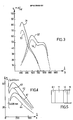
- the curves representative of the efficiency, for each of these wavelengths, are respectively the curves in solid lines 24, 25, 26.
- FIG. 3 indicates respectively, for a layer S 20 and a layer S 25, the spectral sensitivity of structure according to this first embodiment compared to the spectral sensitivity of structure of the prior art comprising respectively the same layer S 20 and the same layer S 25, deposited on ordinary glass.
- the curves relating to the invention are the curves in solid lines 31 and 32 for the layers S 20 and S 25 respectively.
- the curves relating to the prior art are the curves in broken lines respectively 33 and 34.
- the photoemissive layer 12 is bi-alkaline of type Sb K 2 Cs, Sb Rb 2 Cs or mono-alkaline Sb Cs 3
- the substrate 11 is still a glass of high refractive index, glass with lanthanum for example, of index 1.9; the anti-reflection layer 13 being of the known art.
- the curves representative of the photoelectric efficiency p;, as a function of the thickness of the layer are respectively 41, 42 for the structure according to the invention, and 43, 44 for the known art.
- FIG. 5 represents a third embodiment of the invention.
- the structure is provided, on the entry face side of the substrate, with a light scintillator crystal 61 under the action, for example, of X or gamma rays.
- This crystal 61 can have the shape of a blade with parallel faces.
- the crystal as well as the entry face of the photocathode substrate can in fact have very diverse shapes: plane, spherical, concave, convex ...
- Its constituent material has a high refractive index of the order of 1.8, as for example that of chemical formula (Csl, Na), (Csl, TI).
- the structure thus benefits from good optical adaptation to the scintillator / photocathode substrate interface without the use of anti-reflection layers as in the previous embodiments of the invention.
Landscapes
- Physics & Mathematics (AREA)
- Health & Medical Sciences (AREA)
- Life Sciences & Earth Sciences (AREA)
- General Physics & Mathematics (AREA)
- High Energy & Nuclear Physics (AREA)
- Molecular Biology (AREA)
- Spectroscopy & Molecular Physics (AREA)
- Measurement Of Radiation (AREA)
- Photometry And Measurement Of Optical Pulse Characteristics (AREA)
- Light Receiving Elements (AREA)
Applications Claiming Priority (2)
| Application Number | Priority Date | Filing Date | Title |
|---|---|---|---|
| FR8121249A FR2516705A1 (fr) | 1981-11-13 | 1981-11-13 | Structure de detection photoelectrique |
| FR8121249 | 1981-11-13 |
Publications (2)
| Publication Number | Publication Date |
|---|---|
| EP0079651A1 EP0079651A1 (fr) | 1983-05-25 |
| EP0079651B1 true EP0079651B1 (fr) | 1989-07-12 |
Family
ID=9263965
Family Applications (1)
| Application Number | Title | Priority Date | Filing Date |
|---|---|---|---|
| EP82201421A Expired EP0079651B1 (fr) | 1981-11-13 | 1982-11-10 | Structure de détection photoélectrique |
Country Status (5)
| Country | Link |
|---|---|
| US (1) | US4611114A (OSRAM) |
| EP (1) | EP0079651B1 (OSRAM) |
| JP (1) | JPS5896775A (OSRAM) |
| DE (1) | DE3279819D1 (OSRAM) |
| FR (1) | FR2516705A1 (OSRAM) |
Families Citing this family (2)
| Publication number | Priority date | Publication date | Assignee | Title |
|---|---|---|---|---|
| FR2662036B1 (fr) * | 1990-05-14 | 1993-06-25 | Centre Nat Rech Scient | Camera a balayage de fente. |
| CN104076385B (zh) * | 2014-07-04 | 2017-01-04 | 中国科学院高能物理研究所 | γ射线辐射量检测装置及其检测方法 |
Family Cites Families (5)
| Publication number | Priority date | Publication date | Assignee | Title |
|---|---|---|---|---|
| US2768265A (en) * | 1954-04-19 | 1956-10-23 | Jr James R Jenness | Infrared detector cell |
| US2997590A (en) * | 1959-06-26 | 1961-08-22 | Ibm | Infrared radiation entrance window |
| GB1005708A (en) * | 1960-12-14 | 1965-09-29 | Emi Ltd | Improvements relating to photo electrically sensitive devices |
| US4047804A (en) * | 1973-12-26 | 1977-09-13 | Polaroid Corporation | Anti-reflection coatings for photographic bases |
| JPS55129782A (en) * | 1979-03-30 | 1980-10-07 | Hitachi Medical Corp | Radiant ray detector |
-
1981
- 1981-11-13 FR FR8121249A patent/FR2516705A1/fr active Granted
-
1982
- 1982-11-10 EP EP82201421A patent/EP0079651B1/fr not_active Expired
- 1982-11-10 DE DE8282201421T patent/DE3279819D1/de not_active Expired
- 1982-11-12 JP JP57197878A patent/JPS5896775A/ja active Pending
-
1985
- 1985-10-04 US US06/785,087 patent/US4611114A/en not_active Expired - Fee Related
Non-Patent Citations (1)
| Title |
|---|
| JOURNAL OF PHYSICS D: APPLIED PHYSICS, vol. 8, no. 1, 1975, pages 69-84, Letchworth (GB); A.A. DOWMAN et al.: "Scanning electron diffraction studies on alkali antimonide photocathodes, including the S20" * |
Also Published As
| Publication number | Publication date |
|---|---|
| DE3279819D1 (en) | 1989-08-17 |
| FR2516705B1 (OSRAM) | 1984-05-11 |
| FR2516705A1 (fr) | 1983-05-20 |
| EP0079651A1 (fr) | 1983-05-25 |
| US4611114A (en) | 1986-09-09 |
| JPS5896775A (ja) | 1983-06-08 |
Similar Documents
| Publication | Publication Date | Title |
|---|---|---|
| FR2831671A1 (fr) | Detecteur de rayonnement x a l'etat solide | |
| JPH06205768A (ja) | X線検査装置 | |
| EP2583299B1 (fr) | Écran phosphore à fibres optiques comportant un filtre angulaire | |
| EP0428667B1 (fr) | Ecran d'entree de tube intensificateur d'image radiologique | |
| EP0403802B1 (en) | X-ray image intensifier and method of manufacturing input screen | |
| EP0079651B1 (fr) | Structure de détection photoélectrique | |
| EP0056671B1 (fr) | Dispositif de détection photoélectrique | |
| US4914349A (en) | Photo-electric conversion tube with optical fiber plate | |
| EP0319080B1 (fr) | Tube intensificateur d'images à rayons X | |
| EP0540092B1 (fr) | Détecteur d'images à lumière parasite réduite et application à un senseur de terre | |
| EP0013525B1 (fr) | Caméra à scintillation à résolution spatiale améliorée | |
| EP0412887B1 (fr) | Ecran cathodoluminescent à haute efficacité pour tubes à rayons cathodiques haute luminance | |
| FR2768522A1 (fr) | Detecteur a scintillation, revetement refracteur pour scintillateur et procede de fabrication d'un tel revetement | |
| EP0533538B1 (fr) | Tube intensificateur d'image à correction de brillance | |
| EP0182405B1 (fr) | Dispositif photoélectrique pour la détection d'évènements lumineux | |
| WO2025104387A1 (fr) | Photodetecteur comportant une structure a cristal photonique couple optiquement a une couche active a rendement quantique ameliore | |
| Hallensleben et al. | Limitations on the enhancement of photomultiplier quantum efficiency through multiple total internal reflection | |
| Zukic et al. | 30.4-nm narrowband multilayer reflection filters | |
| FR2794565A1 (fr) | Ecran de conversion de rayonnements x en photons lumineux de grande dimension et systeme de radiologie comportant cet ecran |
Legal Events
| Date | Code | Title | Description |
|---|---|---|---|
| PUAI | Public reference made under article 153(3) epc to a published international application that has entered the european phase |
Free format text: ORIGINAL CODE: 0009012 |
|
| 17P | Request for examination filed |
Effective date: 19821110 |
|
| AK | Designated contracting states |
Designated state(s): DE FR GB IT |
|
| GRAA | (expected) grant |
Free format text: ORIGINAL CODE: 0009210 |
|
| AK | Designated contracting states |
Kind code of ref document: B1 Designated state(s): DE FR GB IT |
|
| REF | Corresponds to: |
Ref document number: 3279819 Country of ref document: DE Date of ref document: 19890817 |
|
| ITF | It: translation for a ep patent filed | ||
| GBT | Gb: translation of ep patent filed (gb section 77(6)(a)/1977) | ||
| REG | Reference to a national code |
Ref country code: FR Ref legal event code: CD |
|
| PLBE | No opposition filed within time limit |
Free format text: ORIGINAL CODE: 0009261 |
|
| STAA | Information on the status of an ep patent application or granted ep patent |
Free format text: STATUS: NO OPPOSITION FILED WITHIN TIME LIMIT |
|
| 26N | No opposition filed | ||
| ITTA | It: last paid annual fee | ||
| PGFP | Annual fee paid to national office [announced via postgrant information from national office to epo] |
Ref country code: GB Payment date: 19951101 Year of fee payment: 14 |
|
| PGFP | Annual fee paid to national office [announced via postgrant information from national office to epo] |
Ref country code: FR Payment date: 19951129 Year of fee payment: 14 |
|
| PGFP | Annual fee paid to national office [announced via postgrant information from national office to epo] |
Ref country code: DE Payment date: 19960125 Year of fee payment: 14 |
|
| REG | Reference to a national code |
Ref country code: FR Ref legal event code: CJ Ref country code: FR Ref legal event code: CD |
|
| PG25 | Lapsed in a contracting state [announced via postgrant information from national office to epo] |
Ref country code: GB Effective date: 19961110 |
|
| GBPC | Gb: european patent ceased through non-payment of renewal fee |
Effective date: 19961110 |
|
| PG25 | Lapsed in a contracting state [announced via postgrant information from national office to epo] |
Ref country code: FR Effective date: 19970731 |
|
| PG25 | Lapsed in a contracting state [announced via postgrant information from national office to epo] |
Ref country code: DE Effective date: 19970801 |
|
| REG | Reference to a national code |
Ref country code: FR Ref legal event code: ST |