EP0077874A2 - Image scanner - Google Patents
Image scanner Download PDFInfo
- Publication number
- EP0077874A2 EP0077874A2 EP82103549A EP82103549A EP0077874A2 EP 0077874 A2 EP0077874 A2 EP 0077874A2 EP 82103549 A EP82103549 A EP 82103549A EP 82103549 A EP82103549 A EP 82103549A EP 0077874 A2 EP0077874 A2 EP 0077874A2
- Authority
- EP
- European Patent Office
- Prior art keywords
- array
- image
- electrodes
- radiation
- control electrodes
- Prior art date
- Legal status (The legal status is an assumption and is not a legal conclusion. Google has not performed a legal analysis and makes no representation as to the accuracy of the status listed.)
- Granted
Links
- 239000004020 conductor Substances 0.000 claims abstract description 24
- 230000005855 radiation Effects 0.000 claims abstract description 15
- 238000009825 accumulation Methods 0.000 claims description 7
- 230000010354 integration Effects 0.000 claims description 7
- 230000033001 locomotion Effects 0.000 claims description 6
- 239000004065 semiconductor Substances 0.000 claims description 5
- 230000003287 optical effect Effects 0.000 claims description 4
- 230000009467 reduction Effects 0.000 claims description 2
- 229910021420 polycrystalline silicon Inorganic materials 0.000 abstract description 7
- 229920005591 polysilicon Polymers 0.000 abstract description 7
- XUIMIQQOPSSXEZ-UHFFFAOYSA-N Silicon Chemical compound [Si] XUIMIQQOPSSXEZ-UHFFFAOYSA-N 0.000 abstract description 6
- 229910052710 silicon Inorganic materials 0.000 abstract description 6
- 239000010703 silicon Substances 0.000 abstract description 6
- 239000002184 metal Substances 0.000 abstract description 5
- 238000012546 transfer Methods 0.000 description 15
- 230000035508 accumulation Effects 0.000 description 6
- 238000003491 array Methods 0.000 description 6
- 238000000034 method Methods 0.000 description 4
- NAHBVNMACPIHAH-HLICZWCASA-N p-ii Chemical compound C([C@H]1C(=O)N[C@@H](CCCNC(N)=N)C(=O)N[C@H](C(N[C@H]2CSSC[C@H](NC(=O)[C@H](CC=3C=CC=CC=3)NC(=O)CNC(=O)[C@H](CCCCN)NC(=O)[C@H](CC=3C=CC(O)=CC=3)NC2=O)C(=O)N[C@@H](CC=2C=CC(O)=CC=2)C(=O)N[C@@H](CCCNC(N)=N)C(=O)N[C@@H](CCCCN)C(=O)N[C@@H](CSSC[C@@H](C(=O)N1)NC(=O)[C@H](CC=1C2=CC=CC=C2NC=1)NC(=O)[C@H](CCCNC(N)=N)NC(=O)[C@@H](N)CCCNC(N)=N)C(=O)N[C@@H](CCCNC(N)=N)C(N)=O)=O)C(C)C)C1=CC=CC=C1 NAHBVNMACPIHAH-HLICZWCASA-N 0.000 description 3
- 238000012545 processing Methods 0.000 description 3
- 239000007787 solid Substances 0.000 description 3
- 230000004888 barrier function Effects 0.000 description 2
- 230000004044 response Effects 0.000 description 2
- 230000035945 sensitivity Effects 0.000 description 2
- 230000008719 thickening Effects 0.000 description 2
- 230000009471 action Effects 0.000 description 1
- 230000005540 biological transmission Effects 0.000 description 1
- 230000015556 catabolic process Effects 0.000 description 1
- 230000008878 coupling Effects 0.000 description 1
- 238000010168 coupling process Methods 0.000 description 1
- 238000005859 coupling reaction Methods 0.000 description 1
- 230000001351 cycling effect Effects 0.000 description 1
- 238000006731 degradation reaction Methods 0.000 description 1
- 238000011161 development Methods 0.000 description 1
- 230000000694 effects Effects 0.000 description 1
- 238000004519 manufacturing process Methods 0.000 description 1
- 239000000463 material Substances 0.000 description 1
- 230000005012 migration Effects 0.000 description 1
- 238000013508 migration Methods 0.000 description 1
- 230000008569 process Effects 0.000 description 1
- 230000000750 progressive effect Effects 0.000 description 1
Images

Classifications
-
- H—ELECTRICITY
- H04—ELECTRIC COMMUNICATION TECHNIQUE
- H04N—PICTORIAL COMMUNICATION, e.g. TELEVISION
- H04N1/00—Scanning, transmission or reproduction of documents or the like, e.g. facsimile transmission; Details thereof
- H04N1/024—Details of scanning heads ; Means for illuminating the original
- H04N1/028—Details of scanning heads ; Means for illuminating the original for picture information pick-up
- H04N1/03—Details of scanning heads ; Means for illuminating the original for picture information pick-up with photodetectors arranged in a substantially linear array
- H04N1/0308—Details of scanning heads ; Means for illuminating the original for picture information pick-up with photodetectors arranged in a substantially linear array characterised by the design of the photodetectors, e.g. shape
-
- H—ELECTRICITY
- H01—ELECTRIC ELEMENTS
- H01L—SEMICONDUCTOR DEVICES NOT COVERED BY CLASS H10
- H01L27/00—Devices consisting of a plurality of semiconductor or other solid-state components formed in or on a common substrate
- H01L27/14—Devices consisting of a plurality of semiconductor or other solid-state components formed in or on a common substrate including semiconductor components sensitive to infrared radiation, light, electromagnetic radiation of shorter wavelength or corpuscular radiation and specially adapted either for the conversion of the energy of such radiation into electrical energy or for the control of electrical energy by such radiation
- H01L27/144—Devices controlled by radiation
- H01L27/146—Imager structures
- H01L27/148—Charge coupled imagers
- H01L27/14825—Linear CCD imagers
-
- H—ELECTRICITY
- H01—ELECTRIC ELEMENTS
- H01L—SEMICONDUCTOR DEVICES NOT COVERED BY CLASS H10
- H01L27/00—Devices consisting of a plurality of semiconductor or other solid-state components formed in or on a common substrate
- H01L27/14—Devices consisting of a plurality of semiconductor or other solid-state components formed in or on a common substrate including semiconductor components sensitive to infrared radiation, light, electromagnetic radiation of shorter wavelength or corpuscular radiation and specially adapted either for the conversion of the energy of such radiation into electrical energy or for the control of electrical energy by such radiation
- H01L27/144—Devices controlled by radiation
- H01L27/146—Imager structures
- H01L27/148—Charge coupled imagers
- H01L27/14831—Area CCD imagers
- H01L27/14856—Time-delay and integration
-
- H—ELECTRICITY
- H04—ELECTRIC COMMUNICATION TECHNIQUE
- H04N—PICTORIAL COMMUNICATION, e.g. TELEVISION
- H04N1/00—Scanning, transmission or reproduction of documents or the like, e.g. facsimile transmission; Details thereof
- H04N1/024—Details of scanning heads ; Means for illuminating the original
- H04N1/028—Details of scanning heads ; Means for illuminating the original for picture information pick-up
- H04N1/03—Details of scanning heads ; Means for illuminating the original for picture information pick-up with photodetectors arranged in a substantially linear array
Landscapes
- Engineering & Computer Science (AREA)
- Physics & Mathematics (AREA)
- Power Engineering (AREA)
- General Physics & Mathematics (AREA)
- Electromagnetism (AREA)
- Condensed Matter Physics & Semiconductors (AREA)
- Signal Processing (AREA)
- Multimedia (AREA)
- Computer Hardware Design (AREA)
- Microelectronics & Electronic Packaging (AREA)
- Solid State Image Pick-Up Elements (AREA)
- Facsimile Heads (AREA)
- Image Input (AREA)
Abstract
Description
- This invention relates to image scanners for converting a radiation image pattern into an electronic image.
- Solid state linear scanning arrays are known for the electronic capture of image data from documents or other objects. A linear array inherently requires relative movement with respect to the image source to progressively expose line images which together constitute an image area. Solid state linear arrays currently operate by developing, point-by-point in individual cells of the array, electrical charge proportional to the light exposed to corresponding individual sensing devices. The speed at which images can be processed is limited by the inherent light sensitivy of the sensing devices, as well as the strength of the available light source.
- One known technique for increasing the sensitivity of such a scanner is known as time delay and integration (TDI) which is described, for example, in U.S. 3,833,762 and EP-0030292. A TDI array provides a series of linear arrays whose charge developing cells are coupled in the direction of relative movement of the image, such that the same line is progressively exposed to succeeding ones of the linear arrays. The coupling of the developed arrays enables charge developed by the cells of each array to be transferred to a subsequent cell in the series in a timed relation to the progress of the line image along the series of arrays. This arrangement effectively allows a longer total exposure time of a given line image to sensing devices. In fact, the exposure time can be increased as desired by simply increasing the number of cells in the series to which the line image will be exposed.
- To operate such a TDI array, certain control signals must be applied to the cells to cause the development and transfer of electrical charge at proper times. These signals must be applied at a rate that is related to the speed of progress of the line image relative to the scanner array. Normally, the conductors for applying these signals are made part of the solid state device by use of semi-transparent conductive material such as polysilicon. The transparency of the material is required in order that the control member does not interfere with the reception of light by the underlying photo- sensitive surface. The speed and accuracy with which the control signals can be applied are limited by the relatively low conductivity of the polysilicon, which becomes particularly significant in a TDI array due to the long distances over which the signals must be conducted. The speed of application of the control signals directly limits the permitted speed of the line image relative to the array. The accuracy of the control signal is especially significant in that any error in the transfer of charge causes an accumulated error which can degrade, if not completely destroy, the image being progressively captured.
- This invention is applicable to an image scanner for converting a radiation image pattern into an electronic image, including a time delay and integration array and means for moving the radiation image pattern relative to the array in a first direction, the array including a semiconductor member having a plurality of contiguous photo-sensitive electrical charge holding regions, each region extending in the first direction and having a radiation receptive surface, and a plurality of control electrodes, extending substantially at right angles to the first direction and overlying adjacent portions of the radiation receptive surface of the regions, the control electrodes being capable of conducting both the radiation pattern and electrical current, and control means for applying control voltages to selected control electrodes in synchronism with the relative movement, and is characterised by a plurality of relatively opaque electrical conductors extending angularly across the regions and the control electrodes and interconnecting the control means with the control electrodes.
- Preferably, the conductors are evenly spaced across the surface of the semiconductor member.
- This invention thus employs relatively opaque metal conductors to apply the control signals across the length of a TDI scanning array and orients the conductors angularly across the array to minimize the interference with light and to make such interference as does exist, uniform throughout the array.
- To maintain the array physically as small as possible and still be able to make interconnections reliably between the metal control lines and conductive regions of the sensing device, it is preferred to elongate the light sensing regions in the direction of the relatively short or integration dimension of the array, thus making the sensing regions not square. Because it is usually desirable to sense square picture elements from the document or other image source, an anamorphic lens may be employed to distort square picture elements into an elongated form, similar to the distorted sensing regions, such that the light received by the distorted sensing region actually represents light from a square picture element. The data thus collected will be equivalent to that obtained from square picture element sensing regions imaged through a symmetrical lens.
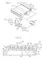
- The scope of the invention is defined by the appended claims; and how it can be carried into effect .is hereinafter particularly described with reference to the accompanying drawings, in which :
- FIGURE 1 is a fragmentary perspective view of a document scanner having a TDI image sensing array, to which the invention is applicable;
- FIGURE 2 is an enlarged pseudo cross-sectional elevational view of the TDI sensing array shown in Figure 1 and taken on the line II-II thereof;
- FIGURE 3 is a plan view of the TDI array shown in Figure 1, and taken on the line III-III thereof, and includes a highly magnified detailed portion illustrating the angle-mounted electrical conductors of the invention; and
- FIGURE 4 is a fragmentary perspective explanatory view showing, in simplified form, the use of an anamorphic lens in a preferred embodiment of the invention.
- An image scanner (Fig.l) includes a document-
feed transport 11 for moving adocument 12 past alight source 13 andlens 14. A time delay and integration (TDI)array 15 receives from lens 14 a projected light or other radiation image represented byarrow 16 of atransverse region 17 extending across the document. As thedocument 12 moves in the direction ofarrow 18, the image ofregion 17 traverses the surface of TDI array 15 in the direction ofarrow 16. As is hereinafter described in detail,TDI array 15 produces, line by line, an electronic analogue image replica of the light image ofdocument 12. This electronic image is transmitted byline 19 to processingcircuitry 20 for utilization by a variety of known techniques unrelated to an understanding of the present invention. Thecircuitry 20 can, for example, be used to create a facsimile image for transmission to a remote location, on to supply an image of character shapes or other patterns for recognition. - Although in
scanner 10 thedocument 12 is moved by a transport, it will be understood that the invention is equally applicable to a system wherein the movingimage 16 is produced through motion of a lens or other optical device. In addition, thearray 15 could itself move with respect to a stationary scene as, for example, in a security surveillance camera that rotates through a viewing arc. - A channel region of array 15 (Fig.2) progressively collects charge in response to a single picture element of a line of
region 17 that is transverse to the transport direction. TheTDI array 15 consists of a silicon body member orwafer 21 that is capable of freeing electrons in response to light. Adjacent to and insulated from the light receptiveupper surface 22 ofwafer 21, is a series of semi-transparent, conductive,charge collection electrodes silicon 21 by the incidence of light in the region of the electrode to be collected adjacent the electrode to a degree proportional to the incidence of light in that region. Semi-transparent, conductive,charge transfer electrodes wafer 21 than are the charge collection electrodes. A positive voltage applied to a charge transfer electrode, such as 31, at a time when voltage is removed from an adjacent charge collection electrode, for example 23, will cause the charge accumulated under thecharge collection electrode 23 to shift laterally throughwafer 21 to a position under thetransfer electrode 31. As shown in Fig.2,transfer electrode 31 is electrically connected to the more closely spacedcharge collection electrode 24 which extends a stronger potential into the surface of thewafer 21 than doeselectrode 31. Thus, the charge moved fromcollection electrode 23 bytransfer electrode 31 continues to move to a position undercharge collection electrode 24. - The
TDI array 15 operates on two phases or alternate operating states (P-I and P-II). Adjacent transfer andcharge collection electrodes control lines Control circuit 40 operates in synchronism with drive motor 41 (Fig.l) fortransport 11 to apply positive voltage alternately tolines silicon wafer 21, in synchronism with the leftward motion of theimage 16. Thus, a line image portion fromregion 17 in Fig.l, which exposes acharge accumulation site 42 of thewafer 21 centred underelectrodes line 38 is positive. Asimage 16 moves leftwardly, voltage is removed fromline 38 and applied toline 39, thus makingcharge transfer electrode 32 effective laterally to attract the charge accumulated byelectrode 24 into the influence ofcharge collection electrode 25 atcharge accumulation site 43 centred underelectrodes line 39 is positive,collection electrode 25 is also collecting additional charge in proportion to the same line image which has now moved leftwardly to be centred onelectrode 25. Subsequently, positive voltage is removed fromline 39 and restored toline 38, so thatcharge transfer electrode 33 attracts the total charge accumulated atelectrode 25 leftwardly, and brings it to chargecollection electrode 26 in synchronism with the further leftward progress ofimage 16. This process continues until the charge that has accumulated through these progressive steps is transferred by charge transfer electrode 37 and deposited under anoutput electrode 44 which, in a known manner, can be one stage of a high-speed shift register from which an entire line of image data can be put ontoline 19 to be supplied to theprocessing circuitry 20. - The rate at which voltage can be applied to and removed from the various electrodes through
lines image 16 that can be successfully tracked. The electrodes are made from polysilicon and extend the length of the scanner array transverse to the cross-sectional view of Fig.2. Connections to these electrodes can be made conventionally at either or both ends of the array, which requires that the voltage be conducted through relatively poor conductors for at least half a length of thearray 15. Increasing the conductivity of the polysilicon electrodes, by either thickening or broadening, is counterproductive beyond a point. Thickening reduces the transparency, thereby making the device less sensitive. Broadening the surface area increases the line capacitance which reduces the permissible accurate cycling rate. These obstacles to increased speed of operation and sensitivity are overcome by the provision ofangled metal conductors - The wafer 21 (Fig.3) is divided by
oxide barrier regions 47 into a plurality ofchannels 48.Barriers 47 limit the sidewise migration of charge and thus define one dimension of a picture element orcharge accumulation site 42 from which light-released electrons are collected. The channels are traversed by theelectrodes opaque conductors conductors 45 are connected to controlline 38, and all of theconductors 46 are connected to controlline 39. Eachconductor 45 is connected atregions 49 to alternate pairs of adjacent transfer and collection electrodes, such as thecharge transfer electrode 32 and thecharge collection electrode 25, and eachconductor 46 is connected atregions 49 to alternate pairs of adjacent transfer and collection electrodes, such as thecharge transfer electrode 31 and thecharge collection electrode 24. It can be seen that the distance required for electrical conduction along the length of the polysilicon electrodes is reduced to essentially half the distance between thelike phase conductors 45. Furthermore, although theconductors upper surface 22 ofsilicon wafer 21, this obstruction is distributed uniformly acrosschannels 48 so as not to cause local degradation or localized loss of the image along the length of the device, because the conductors are evenly spaced across the surface of the array. - It is necessary to have some minimum contact area available between a metal conductor, such as 46, and each pair of polysilicon electrodes, such as 31 and 24, to be able to make the required electrical connection reliably. It is desirable to keep the length of the
silicon wafer 21 as small as possible to simplify manufacturing processes, so that thechannels 48 are narrow. To obtain additional surface area for the purpose of making connections without increasing the length of the scanner array, it is preferred to expand the width of thewafer 21 in the integration direction. This is accomplished by makingwide control electrodes channels 48. Thus, charge-collectingsite 42 is represented by a broken line outline in Fig.3, as that region within achannel 48 that is centred underelectrodes conductor 46. Similar sites are simultaneously created in each of thechannels 48, centred under theelectrodes electrodes site 43 centred underelectrodes - From this description, it can be seen that the light-sensitive areas are significantly elongated in the integration direction, whereas, as mentioned above, it is desirable for most electronic image processing systems to collect images of a symmetrical or square-like character. This result is accomplished through the use of an
anamorphic lens 50. (Fig.4). The anamorphic lens is designed according to known optical techniques used, for example, in the field of cinematography to provide a greater degree of optical reduction along one axis than the other, such that for purposes of my invention, an essentiallysquare area 51 ofregion 17 fromdocument 12 is projected as anelongated area 52 onto the surface ofTDI device 15. The charge accumulated by an elongated site such as 43 will thus be essentially proportional to the light reflected from asquare area 51 of the original document.
Claims (3)
Applications Claiming Priority (2)
| Application Number | Priority Date | Filing Date | Title |
|---|---|---|---|
| US06/313,882 US4375652A (en) | 1981-10-22 | 1981-10-22 | High-speed time delay and integration solid state scanner |
| US313882 | 1981-10-22 |
Publications (3)
| Publication Number | Publication Date |
|---|---|
| EP0077874A2 true EP0077874A2 (en) | 1983-05-04 |
| EP0077874A3 EP0077874A3 (en) | 1986-02-05 |
| EP0077874B1 EP0077874B1 (en) | 1989-07-19 |
Family
ID=23217571
Family Applications (1)
| Application Number | Title | Priority Date | Filing Date |
|---|---|---|---|
| EP82103549A Expired EP0077874B1 (en) | 1981-10-22 | 1982-04-27 | Image scanner |
Country Status (4)
| Country | Link |
|---|---|
| US (1) | US4375652A (en) |
| EP (1) | EP0077874B1 (en) |
| JP (1) | JPS5877255A (en) |
| DE (1) | DE3279832D1 (en) |
Cited By (1)
| Publication number | Priority date | Publication date | Assignee | Title |
|---|---|---|---|---|
| FR2696609A1 (en) * | 1992-10-02 | 1994-04-08 | Sagem | Detector head for facsimile transmission - has aspheric lens converging light rays reflected from printed sheet to array detector |
Families Citing this family (16)
| Publication number | Priority date | Publication date | Assignee | Title |
|---|---|---|---|---|
| JPS5829274A (en) * | 1981-08-14 | 1983-02-21 | Olympus Optical Co Ltd | Image pickup device |
| FR2564674B1 (en) * | 1984-05-18 | 1986-09-19 | Thomson Csf | MULTILINEAR LOAD TRANSFER BAR AND ANALYSIS METHOD |
| US4767927A (en) * | 1984-08-16 | 1988-08-30 | Kabushiki Kaisha Toshiba | Apparatus for reading radiation image information stored in imaging plate |
| NL8501339A (en) * | 1985-05-10 | 1986-12-01 | Philips Nv | SEMICONDUCTOR DEVICE AND METHOD OF MANUFACTURE THEREOF |
| US4703179A (en) * | 1987-04-02 | 1987-10-27 | Ford Aerospace & Communications Corporation | Sensor for hemispherical applications |
| US4877326A (en) | 1988-02-19 | 1989-10-31 | Kla Instruments Corporation | Method and apparatus for optical inspection of substrates |
| USRE36047E (en) * | 1988-09-26 | 1999-01-19 | Picker International, Inc. | Multi-mode TDI/raster-scan television camera system |
| US4954900A (en) * | 1989-01-06 | 1990-09-04 | Ball Corporation | Imaging and wide sector searching apparatus |
| US5646427A (en) * | 1995-08-23 | 1997-07-08 | Dalsa, Inc. | Integrated circuit defect tolerant architecture |
| US5981933A (en) * | 1997-08-26 | 1999-11-09 | Dalsa, Inc. | CCD sensor with diagonal heat conducting straps |
| US6462842B1 (en) | 1998-10-06 | 2002-10-08 | National Semiconductor Corporation | Apparatus, method, and computer program for increasing scanner data throughput |
| US6369918B1 (en) | 1999-02-08 | 2002-04-09 | National Semiconductor Corporation | Apparatus, method, and computer program to reduce distortion of scanner restarts |
| US7046283B1 (en) | 2000-10-11 | 2006-05-16 | Dalsa, Inc. | Arrangements of clock line drivers |
| US7105876B1 (en) | 2001-02-23 | 2006-09-12 | Dalsa, Inc. | Reticulated gate CCD pixel with diagonal strapping |
| GB201019216D0 (en) * | 2010-11-12 | 2010-12-29 | E2V Tech Uk Ltd | Ccd |
| US10903258B2 (en) * | 2017-10-11 | 2021-01-26 | Kla Corporation | Image sensors with grounded or otherwise biased channel-stop contacts |
Citations (2)
| Publication number | Priority date | Publication date | Assignee | Title |
|---|---|---|---|---|
| US3971003A (en) * | 1974-11-18 | 1976-07-20 | Rca Corporation | Charge coupled device imager |
| US4163239A (en) * | 1971-12-30 | 1979-07-31 | Texas Instruments Incorporated | Second level phase lines for CCD line imager |
Family Cites Families (6)
| Publication number | Priority date | Publication date | Assignee | Title |
|---|---|---|---|---|
| US3502802A (en) * | 1966-12-05 | 1970-03-24 | Gen Electric | Solid state scanning system |
| US3833762A (en) * | 1973-06-04 | 1974-09-03 | Rockwell International Corp | Solid state integrating, image motion compensating imager |
| JPS5054283A (en) * | 1973-09-10 | 1975-05-13 | ||
| JPS5413311B2 (en) * | 1974-05-13 | 1979-05-30 | ||
| JPS607390B2 (en) * | 1976-09-17 | 1985-02-23 | 三洋電機株式会社 | Drive pulse power supply method for charge-coupled semiconductor devices |
| FR2456448A1 (en) * | 1979-05-11 | 1980-12-05 | Thomson Csf | DEVICE FOR AUTOMATICALLY CONTROLLING THE TRANSFER FUNCTION OF A VIDEO FREQUENCY TRANSMISSION SYSTEM WITH A VIEW TO IMPROVING IMAGE PERCEPTION |
-
1981
- 1981-10-22 US US06/313,882 patent/US4375652A/en not_active Expired - Fee Related
-
1982
- 1982-04-27 DE DE8282103549T patent/DE3279832D1/en not_active Expired
- 1982-04-27 EP EP82103549A patent/EP0077874B1/en not_active Expired
- 1982-08-05 JP JP57135817A patent/JPS5877255A/en active Granted
Patent Citations (2)
| Publication number | Priority date | Publication date | Assignee | Title |
|---|---|---|---|---|
| US4163239A (en) * | 1971-12-30 | 1979-07-31 | Texas Instruments Incorporated | Second level phase lines for CCD line imager |
| US3971003A (en) * | 1974-11-18 | 1976-07-20 | Rca Corporation | Charge coupled device imager |
Non-Patent Citations (1)
| Title |
|---|
| IBM TECHNICAL DISCLOSURE BULLETIN, vol. 23, no. 12, May 1981, pages 5599-5600, New York, US; S.CHAMBERLAIN et al.: "Time delay and integration imager in GaAs" * |
Cited By (1)
| Publication number | Priority date | Publication date | Assignee | Title |
|---|---|---|---|---|
| FR2696609A1 (en) * | 1992-10-02 | 1994-04-08 | Sagem | Detector head for facsimile transmission - has aspheric lens converging light rays reflected from printed sheet to array detector |
Also Published As
| Publication number | Publication date |
|---|---|
| US4375652A (en) | 1983-03-01 |
| EP0077874A3 (en) | 1986-02-05 |
| EP0077874B1 (en) | 1989-07-19 |
| JPS6226188B2 (en) | 1987-06-08 |
| JPS5877255A (en) | 1983-05-10 |
| DE3279832D1 (en) | 1989-08-24 |
Similar Documents
| Publication | Publication Date | Title |
|---|---|---|
| EP0077874B1 (en) | Image scanner | |
| JPH0135549B2 (en) | ||
| CN100394606C (en) | Light detection device, imaging device and distant image acquisition device | |
| EP0328410A2 (en) | Method for fabricating a solid state imaging device | |
| US6194695B1 (en) | Photoreceptor array for linear optical flow measurement | |
| CA1126944A (en) | Photoelectric rangefinding system using charge transfer devices | |
| EP0093411A2 (en) | Solid state image-sensing device | |
| US4264930A (en) | Charge coupled device incorporating Laplacian thresholding with TDI array | |
| JPS6156912B2 (en) | ||
| US4951106A (en) | Detector device for measuring the intensity of electromagnetic radiation | |
| US3488508A (en) | Solid state image sensor panel | |
| EP0119742B1 (en) | Two-dimensional image readout device | |
| US4553845A (en) | Device for and method of aligning two bodies | |
| US5998794A (en) | Prevention of photoelectric conversion layer contamination in an imaging device | |
| US3938894A (en) | Focus detecting device | |
| US4545684A (en) | Alignment mark detecting apparatus and method | |
| US5332893A (en) | Imaging system and device having a simplified electrode design | |
| US5008696A (en) | Phase difference detecting apparatus | |
| EP0070620A2 (en) | High density imager | |
| US4709381A (en) | CCD focal plane array convolver | |
| US4945377A (en) | Phase difference detecting apparatus | |
| FR2494910B1 (en) | SEMICONDUCTOR DEVICE FOR ELECTRICALLY READING A TWO-DIMENSIONAL IMAGE AND MANUFACTURING METHOD | |
| JPH0572470A (en) | Phase difference detection type focus detection device | |
| JPH0666347B2 (en) | Charge coupled device | |
| JPH0669088B2 (en) | Image input device |
Legal Events
| Date | Code | Title | Description |
|---|---|---|---|
| PUAI | Public reference made under article 153(3) epc to a published international application that has entered the european phase |
Free format text: ORIGINAL CODE: 0009012 |
|
| AK | Designated contracting states |
Designated state(s): DE FR GB |
|
| 17P | Request for examination filed |
Effective date: 19830823 |
|
| PUAL | Search report despatched |
Free format text: ORIGINAL CODE: 0009013 |
|
| AK | Designated contracting states |
Designated state(s): DE FR GB |
|
| 17Q | First examination report despatched |
Effective date: 19870504 |
|
| GRAA | (expected) grant |
Free format text: ORIGINAL CODE: 0009210 |
|
| AK | Designated contracting states |
Kind code of ref document: B1 Designated state(s): DE FR GB |
|
| REF | Corresponds to: |
Ref document number: 3279832 Country of ref document: DE Date of ref document: 19890824 |
|
| ET | Fr: translation filed | ||
| PLBE | No opposition filed within time limit |
Free format text: ORIGINAL CODE: 0009261 |
|
| STAA | Information on the status of an ep patent application or granted ep patent |
Free format text: STATUS: NO OPPOSITION FILED WITHIN TIME LIMIT |
|
| 26N | No opposition filed | ||
| PGFP | Annual fee paid to national office [announced via postgrant information from national office to epo] |
Ref country code: FR Payment date: 19920226 Year of fee payment: 11 |
|
| PGFP | Annual fee paid to national office [announced via postgrant information from national office to epo] |
Ref country code: GB Payment date: 19920304 Year of fee payment: 11 |
|
| PGFP | Annual fee paid to national office [announced via postgrant information from national office to epo] |
Ref country code: DE Payment date: 19920504 Year of fee payment: 11 |
|
| PG25 | Lapsed in a contracting state [announced via postgrant information from national office to epo] |
Ref country code: GB Effective date: 19930427 |
|
| GBPC | Gb: european patent ceased through non-payment of renewal fee |
Effective date: 19930427 |
|
| PG25 | Lapsed in a contracting state [announced via postgrant information from national office to epo] |
Ref country code: FR Effective date: 19931229 |
|
| PG25 | Lapsed in a contracting state [announced via postgrant information from national office to epo] |
Ref country code: DE Effective date: 19940101 |
|
| REG | Reference to a national code |
Ref country code: FR Ref legal event code: ST |