EP0076106A2 - Method for producing a bipolar transistor - Google Patents
Method for producing a bipolar transistor Download PDFInfo
- Publication number
- EP0076106A2 EP0076106A2 EP82305024A EP82305024A EP0076106A2 EP 0076106 A2 EP0076106 A2 EP 0076106A2 EP 82305024 A EP82305024 A EP 82305024A EP 82305024 A EP82305024 A EP 82305024A EP 0076106 A2 EP0076106 A2 EP 0076106A2
- Authority
- EP
- European Patent Office
- Prior art keywords
- layer
- opening
- region
- emitter
- base
- Prior art date
- Legal status (The legal status is an assumption and is not a legal conclusion. Google has not performed a legal analysis and makes no representation as to the accuracy of the status listed.)
- Granted
Links
- 238000004519 manufacturing process Methods 0.000 title claims abstract description 11
- 230000000873 masking effect Effects 0.000 claims abstract description 23
- 230000003064 anti-oxidating effect Effects 0.000 claims abstract description 21
- 239000012535 impurity Substances 0.000 claims abstract description 19
- 229910021420 polycrystalline silicon Inorganic materials 0.000 claims abstract description 11
- 238000005530 etching Methods 0.000 claims abstract description 9
- 238000000034 method Methods 0.000 claims description 29
- 239000004065 semiconductor Substances 0.000 claims description 20
- VYPSYNLAJGMNEJ-UHFFFAOYSA-N Silicium dioxide Chemical compound O=[Si]=O VYPSYNLAJGMNEJ-UHFFFAOYSA-N 0.000 claims description 16
- 239000000758 substrate Substances 0.000 claims description 7
- 239000000377 silicon dioxide Substances 0.000 claims description 6
- 229910052581 Si3N4 Inorganic materials 0.000 claims description 5
- 239000004020 conductor Substances 0.000 claims description 5
- 235000012239 silicon dioxide Nutrition 0.000 claims description 5
- HQVNEWCFYHHQES-UHFFFAOYSA-N silicon nitride Chemical compound N12[Si]34N5[Si]62N3[Si]51N64 HQVNEWCFYHHQES-UHFFFAOYSA-N 0.000 claims description 5
- 238000005229 chemical vapour deposition Methods 0.000 claims description 4
- 238000005121 nitriding Methods 0.000 claims description 2
- 238000000151 deposition Methods 0.000 claims 1
- XUIMIQQOPSSXEZ-UHFFFAOYSA-N Silicon Chemical compound [Si] XUIMIQQOPSSXEZ-UHFFFAOYSA-N 0.000 abstract description 4
- 229910052710 silicon Inorganic materials 0.000 abstract description 4
- 239000010703 silicon Substances 0.000 abstract description 4
- 229920002120 photoresistant polymer Polymers 0.000 description 9
- 238000005468 ion implantation Methods 0.000 description 6
- BASFCYQUMIYNBI-UHFFFAOYSA-N platinum Chemical compound [Pt] BASFCYQUMIYNBI-UHFFFAOYSA-N 0.000 description 6
- 229910052796 boron Inorganic materials 0.000 description 4
- 238000002955 isolation Methods 0.000 description 4
- 229910052814 silicon oxide Inorganic materials 0.000 description 4
- IJGRMHOSHXDMSA-UHFFFAOYSA-N Atomic nitrogen Chemical compound N#N IJGRMHOSHXDMSA-UHFFFAOYSA-N 0.000 description 3
- 230000015572 biosynthetic process Effects 0.000 description 3
- -1 boron ion Chemical class 0.000 description 3
- 230000003647 oxidation Effects 0.000 description 3
- 238000007254 oxidation reaction Methods 0.000 description 3
- 229910052698 phosphorus Inorganic materials 0.000 description 3
- 239000011574 phosphorus Substances 0.000 description 3
- 238000001259 photo etching Methods 0.000 description 3
- 229910052697 platinum Inorganic materials 0.000 description 3
- 238000005406 washing Methods 0.000 description 3
- ZXEYZECDXFPJRJ-UHFFFAOYSA-N $l^{3}-silane;platinum Chemical compound [SiH3].[Pt] ZXEYZECDXFPJRJ-UHFFFAOYSA-N 0.000 description 2
- ZOXJGFHDIHLPTG-UHFFFAOYSA-N Boron Chemical compound [B] ZOXJGFHDIHLPTG-UHFFFAOYSA-N 0.000 description 2
- KRHYYFGTRYWZRS-UHFFFAOYSA-N Fluorane Chemical compound F KRHYYFGTRYWZRS-UHFFFAOYSA-N 0.000 description 2
- OAICVXFJPJFONN-UHFFFAOYSA-N Phosphorus Chemical compound [P] OAICVXFJPJFONN-UHFFFAOYSA-N 0.000 description 2
- XAGFODPZIPBFFR-UHFFFAOYSA-N aluminium Chemical compound [Al] XAGFODPZIPBFFR-UHFFFAOYSA-N 0.000 description 2
- 229910052782 aluminium Inorganic materials 0.000 description 2
- 230000004888 barrier function Effects 0.000 description 2
- 238000009792 diffusion process Methods 0.000 description 2
- 150000002500 ions Chemical class 0.000 description 2
- 229910021339 platinum silicide Inorganic materials 0.000 description 2
- 238000007738 vacuum evaporation Methods 0.000 description 2
- QZPSXPBJTPJTSZ-UHFFFAOYSA-N aqua regia Chemical compound Cl.O[N+]([O-])=O QZPSXPBJTPJTSZ-UHFFFAOYSA-N 0.000 description 1
- 229910052785 arsenic Inorganic materials 0.000 description 1
- RQNWIZPPADIBDY-UHFFFAOYSA-N arsenic atom Chemical compound [As] RQNWIZPPADIBDY-UHFFFAOYSA-N 0.000 description 1
- 229910021419 crystalline silicon Inorganic materials 0.000 description 1
- 238000010438 heat treatment Methods 0.000 description 1
- 230000010354 integration Effects 0.000 description 1
- 239000007788 liquid Substances 0.000 description 1
- 229910052757 nitrogen Inorganic materials 0.000 description 1
- HBMJWWWQQXIZIP-UHFFFAOYSA-N silicon carbide Chemical compound [Si+]#[C-] HBMJWWWQQXIZIP-UHFFFAOYSA-N 0.000 description 1
- 229910010271 silicon carbide Inorganic materials 0.000 description 1
Images

Classifications
-
- H—ELECTRICITY
- H01—ELECTRIC ELEMENTS
- H01L—SEMICONDUCTOR DEVICES NOT COVERED BY CLASS H10
- H01L21/00—Processes or apparatus adapted for the manufacture or treatment of semiconductor or solid state devices or of parts thereof
- H01L21/02—Manufacture or treatment of semiconductor devices or of parts thereof
- H01L21/027—Making masks on semiconductor bodies for further photolithographic processing not provided for in group H01L21/18 or H01L21/34
- H01L21/033—Making masks on semiconductor bodies for further photolithographic processing not provided for in group H01L21/18 or H01L21/34 comprising inorganic layers
-
- H—ELECTRICITY
- H01—ELECTRIC ELEMENTS
- H01L—SEMICONDUCTOR DEVICES NOT COVERED BY CLASS H10
- H01L21/00—Processes or apparatus adapted for the manufacture or treatment of semiconductor or solid state devices or of parts thereof
- H01L21/02—Manufacture or treatment of semiconductor devices or of parts thereof
- H01L21/04—Manufacture or treatment of semiconductor devices or of parts thereof the devices having at least one potential-jump barrier or surface barrier, e.g. PN junction, depletion layer or carrier concentration layer
- H01L21/18—Manufacture or treatment of semiconductor devices or of parts thereof the devices having at least one potential-jump barrier or surface barrier, e.g. PN junction, depletion layer or carrier concentration layer the devices having semiconductor bodies comprising elements of Group IV of the Periodic System or AIIIBV compounds with or without impurities, e.g. doping materials
- H01L21/30—Treatment of semiconductor bodies using processes or apparatus not provided for in groups H01L21/20 - H01L21/26
- H01L21/31—Treatment of semiconductor bodies using processes or apparatus not provided for in groups H01L21/20 - H01L21/26 to form insulating layers thereon, e.g. for masking or by using photolithographic techniques; After treatment of these layers; Selection of materials for these layers
- H01L21/3205—Deposition of non-insulating-, e.g. conductive- or resistive-, layers on insulating layers; After-treatment of these layers
- H01L21/321—After treatment
-
- H—ELECTRICITY
- H01—ELECTRIC ELEMENTS
- H01L—SEMICONDUCTOR DEVICES NOT COVERED BY CLASS H10
- H01L29/00—Semiconductor devices adapted for rectifying, amplifying, oscillating or switching, or capacitors or resistors with at least one potential-jump barrier or surface barrier, e.g. PN junction depletion layer or carrier concentration layer; Details of semiconductor bodies or of electrodes thereof ; Multistep manufacturing processes therefor
- H01L29/66—Types of semiconductor device ; Multistep manufacturing processes therefor
- H01L29/68—Types of semiconductor device ; Multistep manufacturing processes therefor controllable by only the electric current supplied, or only the electric potential applied, to an electrode which does not carry the current to be rectified, amplified or switched
- H01L29/70—Bipolar devices
- H01L29/72—Transistor-type devices, i.e. able to continuously respond to applied control signals
-
- Y—GENERAL TAGGING OF NEW TECHNOLOGICAL DEVELOPMENTS; GENERAL TAGGING OF CROSS-SECTIONAL TECHNOLOGIES SPANNING OVER SEVERAL SECTIONS OF THE IPC; TECHNICAL SUBJECTS COVERED BY FORMER USPC CROSS-REFERENCE ART COLLECTIONS [XRACs] AND DIGESTS
- Y10—TECHNICAL SUBJECTS COVERED BY FORMER USPC
- Y10S—TECHNICAL SUBJECTS COVERED BY FORMER USPC CROSS-REFERENCE ART COLLECTIONS [XRACs] AND DIGESTS
- Y10S438/00—Semiconductor device manufacturing: process
- Y10S438/942—Masking
Definitions
- This invention relates to a semiconductor device and, more particularly, to a method for producing bipolar transistors of an integrated circuit (IC).
- a method for producing a bipolar transistor comprises the steps of selectively etching a silicon oxide layer formed on a base region to form an opening for defining an emitter region, forming an oxide layer containing impurities within the opening and on the silicon oxide layer, diffusing the impurities into the base region out of the impurity-containing oxide layer to form the emitter region, washing out the impurity-containing oxide layer, and forming an emitter electrode.
- the washing out of the impurity-containing oxide layer is carried out by using a suitable etching liquid (e.g.
- the opening for emitter diffusion serves as an emitter electrode opening, so that there is no gap between the position of the emitter electrode opening and that of the emitter region. Accordingly, it is possible to reduce the dimensions of the emitter region to the minimum dimension for etching of the silicon oxide layer.
- the size of the emitter region is made smaller than the conventional emitter region so that the base region and a silicon well (i.e. a silicon island) can be made smaller than the conventional ones.
- the impurities forming the emitter region diffuse in a horizontal direction during the diffusion step, a short between the emitter and base (i.e. a so-called emitter-base short) easily occurs in the bipolar transistor produced by the washed emitter process since the silicon oxide layer is simultaneously etched more or less to enlarge the opening when washing out the impurity-containing oxide layer.
- An object of the present invention is to provide an improved method for producing a bipolar transistor.
- a method for producing a bipolar transistor comprises the steps of forming a semiconductor layer on an anti-oxidation masking layer placed on a base region of a semiconductor body, selectively etching the semiconductor layer to form an opening, introducing impurities into the base region through the opening to form an emitter region, converting the semiconductor layer into an oxide layer whereby the size of the opening is reduced, selectively etching the anti-oxidation masking layer by using the oxide layer as a mask to form an emitter electrode opening and a base electrode opening, and forming electrodes and conductor lines.
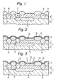
- a semiconductor body 1 comprises a single crystalline silicon (Si) semiconductor substrate 2 and an epitaxial layer 3 grown on the substrate 2.
- the conductivity type of the substrate 2 is, for example, P-type and that of the epitaxial layer 3 is K-type.
- An K -type buried layer 4 is formed in a usual manner in the substrate 2 and the epitaxial layer 3, for example by locally introducing N-type impurities, prior to epitaxial growth, into the substrate 2 and by diffusing the impurities, during epitaxial growth, both into the substrate 2 and into the epitaxial layer 3.
- An anti-oxidation layer consisting of, e.g., silicon nitride (Si 3 N 4 ) is formed on the epitaxial layer 3 of the semiconductor body 1 by a chemical vapor deposition process and then is selectively etched by a photoetching process.
- the epitaxial layer 3 is selectively oxidized to form a thick oxide layer 5 of silicon dioxide (SiO 2 ) by a thermal oxidation process.
- a first photoresist pattern (not shown) is formed on the exposed surface, except for the surface of an isolation-providing region of the epitaxial layer 3.
- P-type impurities e.g., boron
- P-type impurities e.g., boron
- boron ion dose 3 x 10 15 atoms/cm 2 at an energy of 60 keV is used.
- a second photoresist pattern (not shown) is formed on the exposed surface, except for the surface of a collector contact-providing region.
- N-type impurities e.g., phosphorus
- N-type impurities e.g., phosphorus
- a phosphorus ion dose of 2 x 10 15 atoms/cm 2 at an energy of 120 keV is used.
- the semiconductor body 1 is heated (i.e. annealed) at a temperature of e.g. 1150°C for 40 minutes under a dry nitrogen (N ) atmosphere so as to activate the P-type isolation region 6 and the N-type collector region 7.
- the anti-oxidation masking layer is removed with a suitable etchant as illustrated in Fig. 1.
- another anti-oxidation masking layer 8 is formed on at least the base-providing region. It is preferable to form an anti-oxidation masking layer 8 (having a thickness of, e.g., 50 nm) on the exposed surface (i.e., on the thick oxide layer 5, the isolation region 6, the collector contact region 7, and the base-providing region) by the chemical vapor deposition of silicon nitride, as illustrated in Fig. 2.
- the anti-oxidation masking layer (having a thickness of, e.g., 10 nm) by thermally nitriding the exposed surface of the epitaxial layer 3 (i.e.,' the surfaces of the isolation region 6, the collector contact region 7, and the base-providing region).
- the thick oxide layer 5 is not coated with the masking layer.
- a third photoresist layer (not shown) is formed on the exposed surface, except for the surface of a base-providing region.
- P-type impurities e.g., boron
- P-type impurities e.g., boron
- a boron ion dose of 6 x 10 13 atoms/cm 2 at an energy of 40 keV is used.
- the semiconductor body 1 is heated (i.e. annealed) at 900°C for 30 minutes under a dry nitrogen (N 2 ) atmosphere so as to activate the P-type base region 9. It is possible to form the base region 9 prior to the formation of the anti-oxidation masking layer 8.
- a semiconductor layer 10 of polycrystalline silicon having a thickness of, e.g., 150 nm
- a chemical vapor deposition process as illustrated in Fig. 2.
- the polycrystalline silicon layer 10 is selectively etched by a photoetching process to form a first opening 11 for defining an emitter region, a second opening 12 for a base electrode, and a third opening 13 for a collector electrode, as illustrated in Fig. 3.
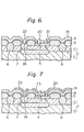
- a photoresist layer 14 is coated on the exposed surface (i.e., on the polycrystalline silicon layer 10 and within the openings 11, 12, and 13) and is selectively removed to form an opening 15 above the first opening 11, and an opening 16 above the third opening 13 as illustrated in Fig. 4.
- N-type impurities donor, e.g., arsenic (As) or phosphorus (P)
- As arsenic
- P phosphorus
- the impurity ions may be implanted by using 60 keV with an ion density of 5 x 10 15 atoms/cm 2 dose. Since the photoresist layer 14 and the polycrystalline silicon layer 10 serve as a mask, the impurities cannot be introduced into the epitaxial layer 3, except for the emitter region 17 and the high doped region 18.
- the polycrystalline silicon layer 10 is converted into an oxide layer 19, as illustrated in Fig. 5.
- the polycrystalline silicon layer 10 is thermally oxidized to form the oxide layer 19 of silicon dioxide by a conventional thermal oxidation process (e.g., at 1000°C for about 50 minutes).
- a conventional thermal oxidation process e.g., at 1000°C for about 50 minutes.
- the volume is increased approximately twofold so that the silicon dioxide layer 19 has a thickness of about 340 nm. Due to such an increase of the volume, the size of the openings 11, 12, and 13 in the polycrystalline silicon layer 10 is reduced to the size of the openings 20, 21, and 22 in the oxide layer 19, respectively.
- the impurities for the emitter region diffuse more or less in a horizontal direction so that the emitter region 17 enlarges. Therefore, the size of the opening 20 is smaller than the size of the emitter region 17.
- the anti-oxidation masking layer 8 is selectively etched with a suitable etchant by using the oxide layer 19 as a mask. Namely, the portions of the masking layer 8 exposed in the openings 20, 21, and 22 are removed to expose portions of the emitter region 17, the base region 8, and the high doped collector contact region 18, as illustrated in Fig. 6.
- the openings 20, 21, and 22 can serve as an emitter electrode opening, a base electrode opening, and a collector electrode opening, respectively.
- a conductor layer of, e.g., aluminum is formed on the exposed surface by vacuum evaporation and is selectively etched by a photoetching process to form an emitter electrode 23, a base electrode 24, and a collector electrode 25, as illustrated in Fig. 7.
- Predetermined conductor lines (not shown) for connecting elements to a circuit are simultaneously formed. It is possible to additionally form a platinum layer (having a thickness of, e.g., 100 nm) on the oxide layer 19 and on the exposed portions of the regions 17, 9, and 18 by a vacuum evaporation process, which platinum layer reacts on the silicon of the exposed portions to form a platinum silicide layer, as a result of being subjected to a heat treatment, prior to the formation of the aluminum layer.
- the platinum silicide can improve the stability of a forward voltage of a schottky barrier diode. After the formation of the electrodes 23, 24, and 25, the platinum layer on the oxide layer 19 is removed with aqua regia by using the electrodes as a mask.
- the emitter electrode opening 20 having smaller dimensions than those of the opening 11 for ion-implantation of the emitter region 17. Therefore, a so-called emitter-base short cannot occur.
- the present invention is not restricted to the above-mentioned embodiments and that many variations are possible for a person having an ordinary skill in the art without departing from the scope of the present invention.
- the anti-oxidation masking layer may be made of silicon carbide instead of silicon nitride.
- tb apply the method according to the present invention to production of an IC comprising bipolar transistors and schottky barrier diodes. In this case, it is possible to easily form an opening for an electrode of a schottky diode as compared with a conventional production method including the washed emitter process.
Abstract
Description
- This invention relates to a semiconductor device and, more particularly, to a method for producing bipolar transistors of an integrated circuit (IC).
- In order to increase the density of an IC or large- scale integration circuit comprising many bipolar transistors, it is proposed to produce a bipolar transistor by a washed emitter process. In the washed emitter process, a method for producing a bipolar transistor comprises the steps of selectively etching a silicon oxide layer formed on a base region to form an opening for defining an emitter region, forming an oxide layer containing impurities within the opening and on the silicon oxide layer, diffusing the impurities into the base region out of the impurity-containing oxide layer to form the emitter region, washing out the impurity-containing oxide layer, and forming an emitter electrode. The washing out of the impurity-containing oxide layer is carried out by using a suitable etching liquid (e.g. hydrofluoric acid) and without using a masking pattern. In the case of the washed emitter process, the opening for emitter diffusion serves as an emitter electrode opening, so that there is no gap between the position of the emitter electrode opening and that of the emitter region. Accordingly, it is possible to reduce the dimensions of the emitter region to the minimum dimension for etching of the silicon oxide layer. Thus, the size of the emitter region is made smaller than the conventional emitter region so that the base region and a silicon well (i.e. a silicon island) can be made smaller than the conventional ones. However, although the impurities forming the emitter region diffuse in a horizontal direction during the diffusion step, a short between the emitter and base (i.e. a so-called emitter-base short) easily occurs in the bipolar transistor produced by the washed emitter process since the silicon oxide layer is simultaneously etched more or less to enlarge the opening when washing out the impurity-containing oxide layer.
- An object of the present invention is to provide an improved method for producing a bipolar transistor.
- According to the present invention, a method for producing a bipolar transistor comprises the steps of forming a semiconductor layer on an anti-oxidation masking layer placed on a base region of a semiconductor body, selectively etching the semiconductor layer to form an opening, introducing impurities into the base region through the opening to form an emitter region, converting the semiconductor layer into an oxide layer whereby the size of the opening is reduced, selectively etching the anti-oxidation masking layer by using the oxide layer as a mask to form an emitter electrode opening and a base electrode opening, and forming electrodes and conductor lines.
- An embodiment of the invention will now be described, by way of example, with reference to the accompanying drawings, in which:
- Figures 1 through 7 are schematic cross-sectional views of a bipolar transistor in various stages of production according to the method of the present invention.
- Referring now to Fig.l, a bipolar transistor in an intermediate stage of production is obtained by the following procedure according to a conventional process. A semiconductor body 1 comprises a single crystalline silicon (Si)
semiconductor substrate 2 and anepitaxial layer 3 grown on thesubstrate 2. The conductivity type of thesubstrate 2 is, for example, P-type and that of theepitaxial layer 3 is K-type. An K -type buriedlayer 4 is formed in a usual manner in thesubstrate 2 and theepitaxial layer 3, for example by locally introducing N-type impurities, prior to epitaxial growth, into thesubstrate 2 and by diffusing the impurities, during epitaxial growth, both into thesubstrate 2 and into theepitaxial layer 3. An anti-oxidation layer (not shown) consisting of, e.g., silicon nitride (Si3N4) is formed on theepitaxial layer 3 of the semiconductor body 1 by a chemical vapor deposition process and then is selectively etched by a photoetching process. Theepitaxial layer 3 is selectively oxidized to form athick oxide layer 5 of silicon dioxide (SiO2) by a thermal oxidation process. A first photoresist pattern (not shown) is formed on the exposed surface, except for the surface of an isolation-providing region of theepitaxial layer 3. P-type impurities (e.g., boron) are introduced into theepitaxial layer 3 through the anti-oxidation masking layer by an ion--implantation process by using the first photoresist pattern as a mask so that anisolation region 6 is formed. For example, a boron ion dose of 3 x 10¹⁵ atoms/cm2 at an energy of 60 keV is used. Then a second photoresist pattern (not shown) is formed on the exposed surface, except for the surface of a collector contact-providing region. N-type impurities (e.g., phosphorus) are also introduced into theepitaxial layer 3 through the anti-oxidation masking layer by an ion-implantation process by using the second photoresist pattern as a mask so that acollector contact region 7 is formed. For example, a phosphorus ion dose of 2 x 10¹⁵ atoms/cm2 at an energy of 120 keV is used. Then, the semiconductor body 1 is heated (i.e. annealed) at a temperature of e.g. 1150°C for 40 minutes under a dry nitrogen (N ) atmosphere so as to activate the P-type isolation region 6 and the N-type collector region 7. The anti-oxidation masking layer is removed with a suitable etchant as illustrated in Fig. 1. - According to the present invention, another
anti-oxidation masking layer 8 is formed on at least the base-providing region. It is preferable to form an anti-oxidation masking layer 8 (having a thickness of, e.g., 50 nm) on the exposed surface (i.e., on thethick oxide layer 5, theisolation region 6, thecollector contact region 7, and the base-providing region) by the chemical vapor deposition of silicon nitride, as illustrated in Fig. 2. It is possible to form the anti-oxidation masking layer (having a thickness of, e.g., 10 nm) by thermally nitriding the exposed surface of the epitaxial layer 3 (i.e.,' the surfaces of theisolation region 6, thecollector contact region 7, and the base-providing region). In this case, thethick oxide layer 5 is not coated with the masking layer. Then a third photoresist layer (not shown) is formed on the exposed surface, except for the surface of a base-providing region. P-type impurities (e.g., boron) are introduced into theepitaxial layer 3 through theanti-oxidation masking layer 8 by an ion-implantation process by using the third photoresist pattern as a mask so that abase region 9 is formed, as illustrated in Fig. 2. For example, a boron ion dose of 6 x 10¹³ atoms/cm 2 at an energy of 40 keV is used. The semiconductor body 1 is heated (i.e. annealed) at 900°C for 30 minutes under a dry nitrogen (N2) atmosphere so as to activate the P-type base region 9. It is possible to form thebase region 9 prior to the formation of theanti-oxidation masking layer 8. Then asemiconductor layer 10 of polycrystalline silicon (having a thickness of, e.g., 150 nm) is formed on theanti-oxidation masking layer 8 by a chemical vapor deposition process, as illustrated in Fig. 2. - The
polycrystalline silicon layer 10 is selectively etched by a photoetching process to form a first opening 11 for defining an emitter region, asecond opening 12 for a base electrode, and athird opening 13 for a collector electrode, as illustrated in Fig. 3. - A
photoresist layer 14 is coated on the exposed surface (i.e., on thepolycrystalline silicon layer 10 and within theopenings 11, 12, and 13) and is selectively removed to form anopening 15 above the first opening 11, and anopening 16 above the third opening 13 as illustrated in Fig. 4. N-type impurities (donor, e.g., arsenic (As) or phosphorus (P)) are introduced into thebase region 9 through the opening 15, the first opening 11, and theanti-oxidation masking layer 8 by an ion-implantation process to form theemitter region 17. Simultaneously a high dopedcollector contact region 18 is formed in theregion 7 by the ion-implantation process. The impurity ions may be implanted by using 60 keV with an ion density of 5 x 10¹⁵ atoms/cm2 dose. Since thephotoresist layer 14 and thepolycrystalline silicon layer 10 serve as a mask, the impurities cannot be introduced into theepitaxial layer 3, except for theemitter region 17 and the highdoped region 18. - After removing the
photoresist layer 14, thepolycrystalline silicon layer 10 is converted into anoxide layer 19, as illustrated in Fig. 5. Practically, thepolycrystalline silicon layer 10 is thermally oxidized to form theoxide layer 19 of silicon dioxide by a conventional thermal oxidation process (e.g., at 1000°C for about 50 minutes). When polycrystalline silicon is converted into silicon dioxide, the volume is increased approximately twofold so that thesilicon dioxide layer 19 has a thickness of about 340 nm. Due to such an increase of the volume, the size of theopenings polycrystalline silicon layer 10 is reduced to the size of theopenings oxide layer 19, respectively. Furthermore, during thermal oxidation, the impurities for the emitter region diffuse more or less in a horizontal direction so that theemitter region 17 enlarges. Therefore, the size of the opening 20 is smaller than the size of theemitter region 17. - The
anti-oxidation masking layer 8 is selectively etched with a suitable etchant by using theoxide layer 19 as a mask. Namely, the portions of themasking layer 8 exposed in theopenings emitter region 17, thebase region 8, and the high dopedcollector contact region 18, as illustrated in Fig. 6. Thus, theopenings - Then a conductor layer of, e.g., aluminum is formed on the exposed surface by vacuum evaporation and is selectively etched by a photoetching process to form an
emitter electrode 23, abase electrode 24, and acollector electrode 25, as illustrated in Fig. 7. Predetermined conductor lines (not shown) for connecting elements to a circuit are simultaneously formed. It is possible to additionally form a platinum layer (having a thickness of, e.g., 100 nm) on theoxide layer 19 and on the exposed portions of theregions electrodes oxide layer 19 is removed with aqua regia by using the electrodes as a mask. - According to the present invention, it is possible to form by self-alignment the emitter electrode opening 20 having smaller dimensions than those of the opening 11 for ion-implantation of the
emitter region 17. Therefore, a so-called emitter-base short cannot occur. - It will be obvious that the present invention is not restricted to the above-mentioned embodiments and that many variations are possible for a person having an ordinary skill in the art without departing from the scope of the present invention. For example, it is possible to produce a PNP-type bipolar transistor instead of the above-mentioned NPN-type bipolar transistor, and the anti-oxidation masking layer may be made of silicon carbide instead of silicon nitride. It is preferable tb apply the method according to the present invention to production of an IC comprising bipolar transistors and schottky barrier diodes. In this case, it is possible to easily form an opening for an electrode of a schottky diode as compared with a conventional production method including the washed emitter process.
Claims (7)
Applications Claiming Priority (2)
| Application Number | Priority Date | Filing Date | Title |
|---|---|---|---|
| JP151986/81 | 1981-09-28 | ||
| JP56151986A JPS5870570A (en) | 1981-09-28 | 1981-09-28 | Manufacture of semiconductor device |
Publications (3)
| Publication Number | Publication Date |
|---|---|
| EP0076106A2 true EP0076106A2 (en) | 1983-04-06 |
| EP0076106A3 EP0076106A3 (en) | 1985-01-23 |
| EP0076106B1 EP0076106B1 (en) | 1987-08-12 |
Family
ID=15530556
Family Applications (1)
| Application Number | Title | Priority Date | Filing Date |
|---|---|---|---|
| EP82305024A Expired EP0076106B1 (en) | 1981-09-28 | 1982-09-23 | Method for producing a bipolar transistor |
Country Status (4)
| Country | Link |
|---|---|
| US (1) | US4408387A (en) |
| EP (1) | EP0076106B1 (en) |
| JP (1) | JPS5870570A (en) |
| DE (1) | DE3276978D1 (en) |
Cited By (1)
| Publication number | Priority date | Publication date | Assignee | Title |
|---|---|---|---|---|
| EP0242893A1 (en) * | 1986-03-26 | 1987-10-28 | Koninklijke Philips Electronics N.V. | Method of manufacturing a semiconductor device |
Families Citing this family (17)
| Publication number | Priority date | Publication date | Assignee | Title |
|---|---|---|---|---|
| JPS5975659A (en) * | 1982-10-22 | 1984-04-28 | Fujitsu Ltd | Manufacture of semiconductor device |
| US4498227A (en) * | 1983-07-05 | 1985-02-12 | Fairchild Camera & Instrument Corporation | Wafer fabrication by implanting through protective layer |
| JPS6045052A (en) * | 1983-08-22 | 1985-03-11 | Mitsubishi Electric Corp | Semiconductor integrated circuit device |
| US4566176A (en) * | 1984-05-23 | 1986-01-28 | U.S. Philips Corporation | Method of manufacturing transistors |
| JPS6146063A (en) * | 1984-08-10 | 1986-03-06 | Hitachi Ltd | Manufacture of semiconductor device |
| US4721682A (en) * | 1985-09-25 | 1988-01-26 | Monolithic Memories, Inc. | Isolation and substrate connection for a bipolar integrated circuit |
| JPS63107167A (en) * | 1986-10-24 | 1988-05-12 | Oki Electric Ind Co Ltd | Manufacture of semiconductor integrated circuit device |
| US4855798A (en) * | 1986-12-19 | 1989-08-08 | Texas Instruments Incorporated | Semiconductor and process of fabrication thereof |
| US5270252A (en) * | 1988-10-25 | 1993-12-14 | United States Of America As Represented By The Secretary Of The Navy | Method of forming platinum and platinum silicide schottky contacts on beta-silicon carbide |
| JP2871530B2 (en) * | 1995-05-10 | 1999-03-17 | 日本電気株式会社 | Method for manufacturing semiconductor device |
| US5702959A (en) * | 1995-05-31 | 1997-12-30 | Texas Instruments Incorporated | Method for making an isolated vertical transistor |
| US5872052A (en) * | 1996-02-12 | 1999-02-16 | Micron Technology, Inc. | Planarization using plasma oxidized amorphous silicon |
| KR100275962B1 (en) | 1998-12-30 | 2001-02-01 | 김영환 | Semiconductor device and manufacturing method thereof |
| US20060054183A1 (en) * | 2004-08-27 | 2006-03-16 | Thomas Nowak | Method to reduce plasma damage during cleaning of semiconductor wafer processing chamber |
| US20060090773A1 (en) * | 2004-11-04 | 2006-05-04 | Applied Materials, Inc. | Sulfur hexafluoride remote plasma source clean |
| US8338906B2 (en) * | 2008-01-30 | 2012-12-25 | Taiwan Semiconductor Manufacturing Co., Ltd. | Schottky device |
| USD848384S1 (en) * | 2017-08-17 | 2019-05-14 | Epistar Corporation | Transistor |
Citations (4)
| Publication number | Priority date | Publication date | Assignee | Title |
|---|---|---|---|---|
| FR2347778A1 (en) * | 1976-04-05 | 1977-11-04 | Ibm | PROCESS FOR FORMING AN INTEGRATED CIRCUIT REGION BY THE COMBINATION OF IONIC IMPLEMENTATION AND DIFFUSION STAGES |
| FR2389236A1 (en) * | 1977-04-25 | 1978-11-24 | Nippon Telegraph & Telephone | BIPOLAR TRANSISTORS AND MANUFACTURING PROCESS |
| US4242791A (en) * | 1979-09-21 | 1981-01-06 | International Business Machines Corporation | High performance bipolar transistors fabricated by post emitter base implantation process |
| EP0036082A1 (en) * | 1980-03-13 | 1981-09-23 | International Business Machines Corporation | A self-aligned process for providing an improved high performance bipolar transistor |
Family Cites Families (6)
| Publication number | Priority date | Publication date | Assignee | Title |
|---|---|---|---|---|
| US3507716A (en) * | 1966-09-02 | 1970-04-21 | Hitachi Ltd | Method of manufacturing semiconductor device |
| US3710204A (en) * | 1967-05-20 | 1973-01-09 | Telefunken Patent | A semiconductor device having a screen electrode of intrinsic semiconductor material |
| US3909925A (en) * | 1974-05-06 | 1975-10-07 | Telex Computer Products | N-Channel charge coupled device fabrication process |
| DE2605641C3 (en) * | 1976-02-12 | 1979-12-20 | Siemens Ag, 1000 Berlin Und 8000 Muenchen | High frequency transistor and process for its manufacture |
| US4266985A (en) * | 1979-05-18 | 1981-05-12 | Fujitsu Limited | Process for producing a semiconductor device including an ion implantation step in combination with direct thermal nitridation of the silicon substrate |
| US4376664A (en) * | 1979-05-31 | 1983-03-15 | Fujitsu Limited | Method of producing a semiconductor device |
-
1981
- 1981-09-28 JP JP56151986A patent/JPS5870570A/en active Granted
-
1982
- 1982-09-23 EP EP82305024A patent/EP0076106B1/en not_active Expired
- 1982-09-23 DE DE8282305024T patent/DE3276978D1/en not_active Expired
- 1982-09-28 US US06/425,648 patent/US4408387A/en not_active Expired - Fee Related
Patent Citations (4)
| Publication number | Priority date | Publication date | Assignee | Title |
|---|---|---|---|---|
| FR2347778A1 (en) * | 1976-04-05 | 1977-11-04 | Ibm | PROCESS FOR FORMING AN INTEGRATED CIRCUIT REGION BY THE COMBINATION OF IONIC IMPLEMENTATION AND DIFFUSION STAGES |
| FR2389236A1 (en) * | 1977-04-25 | 1978-11-24 | Nippon Telegraph & Telephone | BIPOLAR TRANSISTORS AND MANUFACTURING PROCESS |
| US4242791A (en) * | 1979-09-21 | 1981-01-06 | International Business Machines Corporation | High performance bipolar transistors fabricated by post emitter base implantation process |
| EP0036082A1 (en) * | 1980-03-13 | 1981-09-23 | International Business Machines Corporation | A self-aligned process for providing an improved high performance bipolar transistor |
Cited By (1)
| Publication number | Priority date | Publication date | Assignee | Title |
|---|---|---|---|---|
| EP0242893A1 (en) * | 1986-03-26 | 1987-10-28 | Koninklijke Philips Electronics N.V. | Method of manufacturing a semiconductor device |
Also Published As
| Publication number | Publication date |
|---|---|
| JPS6153867B2 (en) | 1986-11-19 |
| US4408387A (en) | 1983-10-11 |
| JPS5870570A (en) | 1983-04-27 |
| EP0076106A3 (en) | 1985-01-23 |
| DE3276978D1 (en) | 1987-09-17 |
| EP0076106B1 (en) | 1987-08-12 |
Similar Documents
| Publication | Publication Date | Title |
|---|---|---|
| US4299024A (en) | Fabrication of complementary bipolar transistors and CMOS devices with poly gates | |
| EP0100897B1 (en) | Method for contacting a pn junction region | |
| EP0076106B1 (en) | Method for producing a bipolar transistor | |
| US4437897A (en) | Fabrication process for a shallow emitter/base transistor using same polycrystalline layer | |
| JPS62588B2 (en) | ||
| US4151006A (en) | Method of manufacturing a semiconductor device | |
| EP0314600B1 (en) | Self-aligned polysilicon emitter and contact structure for high performance bipolar transistors | |
| EP0199497B1 (en) | Process for fabricating a self-aligned bipolar transistor | |
| US4824794A (en) | Method for fabricating a bipolar transistor having self aligned base and emitter | |
| GB1587398A (en) | Semiconductor device manufacture | |
| KR870006673A (en) | Fabrication process of self-aligned bipolar transistor structure | |
| US4191595A (en) | Method of manufacturing PN junctions in a semiconductor region to reach an isolation layer without exposing the semiconductor region surface | |
| US4525922A (en) | Method of producing a semiconductor device | |
| JPH0241170B2 (en) | ||
| US4669178A (en) | Process for forming a self-aligned low resistance path in semiconductor devices | |
| US4546537A (en) | Method for producing a semiconductor device utilizing V-groove etching and thermal oxidation | |
| EP0378164A2 (en) | Bipolar transistor and method of manufacturing the same | |
| JPS6330787B2 (en) | ||
| JP2677258B2 (en) | Semiconductor device and manufacturing method thereof | |
| JP2546650B2 (en) | Method of manufacturing bipolar transistor | |
| JPH0579186B2 (en) | ||
| JPH02304931A (en) | Semiconductor device and manufacture thereof | |
| JPH061815B2 (en) | Method for manufacturing semiconductor device | |
| KR19980036830A (en) | Bipolar Junction Transistor Manufacturing Method | |
| JPS6346769A (en) | Manufacture of semiconductor device |
Legal Events
| Date | Code | Title | Description |
|---|---|---|---|
| PUAI | Public reference made under article 153(3) epc to a published international application that has entered the european phase |
Free format text: ORIGINAL CODE: 0009012 |
|
| AK | Designated contracting states |
Designated state(s): DE FR GB |
|
| PUAL | Search report despatched |
Free format text: ORIGINAL CODE: 0009013 |
|
| AK | Designated contracting states |
Designated state(s): DE FR GB |
|
| 17P | Request for examination filed |
Effective date: 19850709 |
|
| 17Q | First examination report despatched |
Effective date: 19861027 |
|
| GRAA | (expected) grant |
Free format text: ORIGINAL CODE: 0009210 |
|
| AK | Designated contracting states |
Kind code of ref document: B1 Designated state(s): DE FR GB |
|
| ET | Fr: translation filed | ||
| REF | Corresponds to: |
Ref document number: 3276978 Country of ref document: DE Date of ref document: 19870917 |
|
| PLBE | No opposition filed within time limit |
Free format text: ORIGINAL CODE: 0009261 |
|
| STAA | Information on the status of an ep patent application or granted ep patent |
Free format text: STATUS: NO OPPOSITION FILED WITHIN TIME LIMIT |
|
| 26N | No opposition filed | ||
| PGFP | Annual fee paid to national office [announced via postgrant information from national office to epo] |
Ref country code: GB Payment date: 19920911 Year of fee payment: 11 |
|
| PGFP | Annual fee paid to national office [announced via postgrant information from national office to epo] |
Ref country code: FR Payment date: 19920929 Year of fee payment: 11 |
|
| PGFP | Annual fee paid to national office [announced via postgrant information from national office to epo] |
Ref country code: DE Payment date: 19921125 Year of fee payment: 11 |
|
| PG25 | Lapsed in a contracting state [announced via postgrant information from national office to epo] |
Ref country code: GB Effective date: 19930923 |
|
| GBPC | Gb: european patent ceased through non-payment of renewal fee |
Effective date: 19930923 |
|
| PG25 | Lapsed in a contracting state [announced via postgrant information from national office to epo] |
Ref country code: FR Free format text: LAPSE BECAUSE OF NON-PAYMENT OF DUE FEES Effective date: 19940531 |
|
| PG25 | Lapsed in a contracting state [announced via postgrant information from national office to epo] |
Ref country code: DE Effective date: 19940601 |
|
| REG | Reference to a national code |
Ref country code: FR Ref legal event code: ST |