EP0075382A1 - Power supply for arc lamps - Google Patents
Power supply for arc lamps Download PDFInfo
- Publication number
- EP0075382A1 EP0075382A1 EP82303612A EP82303612A EP0075382A1 EP 0075382 A1 EP0075382 A1 EP 0075382A1 EP 82303612 A EP82303612 A EP 82303612A EP 82303612 A EP82303612 A EP 82303612A EP 0075382 A1 EP0075382 A1 EP 0075382A1
- Authority
- EP
- European Patent Office
- Prior art keywords
- oscillator
- power supply
- circuit
- voltage
- supply
- Prior art date
- Legal status (The legal status is an assumption and is not a legal conclusion. Google has not performed a legal analysis and makes no representation as to the accuracy of the status listed.)
- Granted
Links
Images


Classifications
-
- H—ELECTRICITY
- H02—GENERATION; CONVERSION OR DISTRIBUTION OF ELECTRIC POWER
- H02M—APPARATUS FOR CONVERSION BETWEEN AC AND AC, BETWEEN AC AND DC, OR BETWEEN DC AND DC, AND FOR USE WITH MAINS OR SIMILAR POWER SUPPLY SYSTEMS; CONVERSION OF DC OR AC INPUT POWER INTO SURGE OUTPUT POWER; CONTROL OR REGULATION THEREOF
- H02M7/00—Conversion of ac power input into dc power output; Conversion of dc power input into ac power output
- H02M7/42—Conversion of dc power input into ac power output without possibility of reversal
- H02M7/44—Conversion of dc power input into ac power output without possibility of reversal by static converters
- H02M7/48—Conversion of dc power input into ac power output without possibility of reversal by static converters using discharge tubes with control electrode or semiconductor devices with control electrode
- H02M7/53—Conversion of dc power input into ac power output without possibility of reversal by static converters using discharge tubes with control electrode or semiconductor devices with control electrode using devices of a triode or transistor type requiring continuous application of a control signal
- H02M7/537—Conversion of dc power input into ac power output without possibility of reversal by static converters using discharge tubes with control electrode or semiconductor devices with control electrode using devices of a triode or transistor type requiring continuous application of a control signal using semiconductor devices only, e.g. single switched pulse inverters
- H02M7/5387—Conversion of dc power input into ac power output without possibility of reversal by static converters using discharge tubes with control electrode or semiconductor devices with control electrode using devices of a triode or transistor type requiring continuous application of a control signal using semiconductor devices only, e.g. single switched pulse inverters in a bridge configuration
-
- H—ELECTRICITY
- H05—ELECTRIC TECHNIQUES NOT OTHERWISE PROVIDED FOR
- H05B—ELECTRIC HEATING; ELECTRIC LIGHT SOURCES NOT OTHERWISE PROVIDED FOR; CIRCUIT ARRANGEMENTS FOR ELECTRIC LIGHT SOURCES, IN GENERAL
- H05B41/00—Circuit arrangements or apparatus for igniting or operating discharge lamps
- H05B41/14—Circuit arrangements
- H05B41/26—Circuit arrangements in which the lamp is fed by power derived from dc by means of a converter, e.g. by high-voltage dc
- H05B41/28—Circuit arrangements in which the lamp is fed by power derived from dc by means of a converter, e.g. by high-voltage dc using static converters
- H05B41/288—Circuit arrangements in which the lamp is fed by power derived from dc by means of a converter, e.g. by high-voltage dc using static converters with semiconductor devices and specially adapted for lamps without preheating electrodes, e.g. for high-intensity discharge lamps, high-pressure mercury or sodium lamps or low-pressure sodium lamps
- H05B41/2885—Static converters especially adapted therefor; Control thereof
- H05B41/2887—Static converters especially adapted therefor; Control thereof characterised by a controllable bridge in the final stage
-
- H—ELECTRICITY
- H05—ELECTRIC TECHNIQUES NOT OTHERWISE PROVIDED FOR
- H05B—ELECTRIC HEATING; ELECTRIC LIGHT SOURCES NOT OTHERWISE PROVIDED FOR; CIRCUIT ARRANGEMENTS FOR ELECTRIC LIGHT SOURCES, IN GENERAL
- H05B41/00—Circuit arrangements or apparatus for igniting or operating discharge lamps
- H05B41/14—Circuit arrangements
- H05B41/26—Circuit arrangements in which the lamp is fed by power derived from dc by means of a converter, e.g. by high-voltage dc
- H05B41/28—Circuit arrangements in which the lamp is fed by power derived from dc by means of a converter, e.g. by high-voltage dc using static converters
- H05B41/288—Circuit arrangements in which the lamp is fed by power derived from dc by means of a converter, e.g. by high-voltage dc using static converters with semiconductor devices and specially adapted for lamps without preheating electrodes, e.g. for high-intensity discharge lamps, high-pressure mercury or sodium lamps or low-pressure sodium lamps
- H05B41/292—Arrangements for protecting lamps or circuits against abnormal operating conditions
- H05B41/2921—Arrangements for protecting lamps or circuits against abnormal operating conditions for protecting the circuit against abnormal operating conditions
-
- Y—GENERAL TAGGING OF NEW TECHNOLOGICAL DEVELOPMENTS; GENERAL TAGGING OF CROSS-SECTIONAL TECHNOLOGIES SPANNING OVER SEVERAL SECTIONS OF THE IPC; TECHNICAL SUBJECTS COVERED BY FORMER USPC CROSS-REFERENCE ART COLLECTIONS [XRACs] AND DIGESTS
- Y02—TECHNOLOGIES OR APPLICATIONS FOR MITIGATION OR ADAPTATION AGAINST CLIMATE CHANGE
- Y02B—CLIMATE CHANGE MITIGATION TECHNOLOGIES RELATED TO BUILDINGS, e.g. HOUSING, HOUSE APPLIANCES OR RELATED END-USER APPLICATIONS
- Y02B20/00—Energy efficient lighting technologies, e.g. halogen lamps or gas discharge lamps
-
- Y—GENERAL TAGGING OF NEW TECHNOLOGICAL DEVELOPMENTS; GENERAL TAGGING OF CROSS-SECTIONAL TECHNOLOGIES SPANNING OVER SEVERAL SECTIONS OF THE IPC; TECHNICAL SUBJECTS COVERED BY FORMER USPC CROSS-REFERENCE ART COLLECTIONS [XRACs] AND DIGESTS
- Y10—TECHNICAL SUBJECTS COVERED BY FORMER USPC
- Y10S—TECHNICAL SUBJECTS COVERED BY FORMER USPC CROSS-REFERENCE ART COLLECTIONS [XRACs] AND DIGESTS
- Y10S315/00—Electric lamp and discharge devices: systems
- Y10S315/07—Starting and control circuits for gas discharge lamp using transistors
Definitions
- This invention relates to power supplies for arc lamps and more particularly to a power supply for a metal halide are lamp such as a mercury, iodine lamp, used to provide daylight and other spectrum lighting, for example, for cinematographic stages, outside television broadcasts and the like.
- a metal halide are lamp such as a mercury, iodine lamp, used to provide daylight and other spectrum lighting, for example, for cinematographic stages, outside television broadcasts and the like.
- Arc lamps of the kind referred to are preferably driven by A.C. since D.C. drive causes rapid erosion of the lamp electrodes. If driven by a sinusoidal current waveform the lamp produces a white light level which is modulated rather than constant as required. This effect arises because, as the supply current passes through zero, the arc gases cool and reheat, the arc being maintained by its thermal inertia, with the result that the light emission from the arc varies. If the lamp is driven by a square current waveform, the speed of passage of the current through zero is greatly increased and modulation of the light output of the arc is greatly reduced.
- a power supply for a metal halide arc lamp which consists of a bridge network of switching transistors to provide a square current waveform for driving the arc, the bridge being connected to the supply by way of a series bank of resistors, the supply being either a D.C. generator or a rectified mains supply.
- a power supply is of appreciable bulk primarily because of the size of heat sinks required to dissipate heat generated in the resistor bank and is for that reason expensive to construct. Transportation of the power supply to the location where it is used, moreover, is tedious and expensive.
- the present invention consists in a power supply for an arc lamp, comprising a power source and an inverter, characterised in that the power source is a constant current source for the supply of current to the inverter and the inverter is a bridge network of field effect transistor ' s and an oscillator adapted to supply square wave voltage switching pulses to the transistors, whereby the bridge network affords an output current of alternating square pulses of current of equal duration for driving the lamp.
- the field effect transistors are insulated gate devices supplied with gate to source voltages by way of opto-isolators from the oscillator.
- the constant current source comprises an inductor provided with a free wheel diode for connection to a D.C. voltage source and through which current is drawn by a field effect transistor, the current level through which is employed to control the ratio of 'on' to 'off' time of a chopper oscillator supplying the gate to source voltage of the transistor.
- the current level through the field effect transistor is employed to switch a junction transistor, conduction of which inhibits the oscillator.
- the constant current source and bridge network are mounted on a single circuit board and constitute a power module for parallel connection of the current source input terminals and bridge network output terminals with corresponding terminals of one or more further like power modules.
- the oscillator for the supply of square voltage switching pulses to the bridge network is mounted as a module on a circuit board which is adapted for connection to the power modules to serve as a common oscillator for the field effect transistor bridge networks thereof.
- the common oscillator module further carries a plurality of system protection circuits, a supply circuit for supplying stabilised voltages to the constant current source, the common oscillator, the bridge network and the protection circuits, and a control circuit adapted upon triggering of any of the protection circuits to disconnect the mains power supply from the power modules.
- the power supply according to the invention represents a considerable saving in weight as compared with the prior art arrangements and is cheaper to construct. It can be used without modification of the electronic circuitry with normally available power sources such as 110 volts 60 cycles per second, and 220 volts 50 cycles per second and 120 volts D.C.
- the modular construction and ability to connect modules in parallel makes the invention readily adaptable for use with lamps of different power.
- the use of field effect transistors considerably simplifies the circuitry and enables the modular concept to be implemented with less difficulty than would be the case with bridge circuits employing junction transistors.
- Junction transistors have considerable disadvantages as compared with field effect transistors when used in an inverter bridge of a power supply.
- field effect transistors conduct when a voltage is applied between their gate and source terminals and need only a buffer stage between an oscillator supplying that voltage and the gate and source terminals.
- Bipolar junction transistors on the other hand require relatively high drive current to bring them into full conduction and further require special protection to guard against secondary breakdown and thermal runaway.
- the drive circuitry for the field effect transistors is accordingly considerably simplified as compared with that of bipolar transistors and lower switching losses are entailed when field effect transistors are employed.
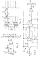
- the power supply circuit therein illustrated consists of a constant current source 1 contained in the area enclosed by broken lines 3 and a bridge inverter circuit 2 enclosed by broken lines 4.
- the constant current source 1 consists of a power supply 5 adapted for use with 110 volt or 220 volt, 50 Hertz supplies and to that end comprises two series connected smoothing capacitors 6 and 7 across which the D.C. output voltage of the power supply 5 is developed.
- Input terminals of the supply 5 comprise live, neutral and earth terminals 8, 9 and 10 respectively, of which terminal 10 is connected to the casing in which the circuits illustrated in the drawings are accommodated.
- Live terminal 8 is connected by way of a 220 volt link 11, fuse 12 and diode 13 to the side of capacitor 6 remote from the common point thereof with capacitor 7 and by way of link 11 fuse 12 and diode 14 to the side of capacitor 7 remote from the common point thereof with capacitor 6.
- diode 15 which connects with neutral terminal 9 by way of a thermistor 17.
- a diode 16 is also serially connected by way of the thermistor 17 between terminal 9 and the side of capacitor 7 to which is connected diode 14 and a diode 15 is connected to the common point of diode 16 and thermistor 17.
- the diodes 13,14,15 and 16 are poled to form a diode bridge network the input of which consists of the live and neutral terminals 8 and 9 whilst the output comprises the series connected capacitors 6 and 7.
- the thermistor 17 has a high resistance at low temperature and thus serves to limit surge currents at start up.
- the live terminal 8 is also connected by a 110 volt link 18 and fuse 19 to the common point of capacitors 6 and 7.
- the series voltage of the output capacitors 6 and 7 is substantially the sum of the fully charged voltages of those capacitors and constitutes the D.C. rectified output voltage provided at rails 20 and 21 of the constant current source 1.
- the rails 20 and 21 supply a choke 22 through which current can be drawn by a field effect transistor 23 of the insulated gate type.
- the transistor 23 is driven by a chopper oscillator 24 which consists of stages 25 and 26 and constitutes a known form of digital integrated circuit (typically RCA COS/MOS type CD 4041A).
- the oscillator is supplied by a 12 volt voltage rail 27 and positive feedback is afforded by capacitor 28.
- the gate to source voltage of the field effect transistor 23 is supplied from the oscillator 24 by way of a buffer stage 29 and a field effect transistor 30, the latter forming part of the chopper oscillator failure detection circuit hereinafter referred to with reference particularly to Figure 5.
- the choke 35 serves to protect the bridge circuit 2 by preventing the capacitor 34 from discharging into field effect transistors 36 to 39 forming that bridge circuit and it further serves to protect the chopper oscillator 24 by absorbing voltage spikes when the bridge circuit is initially switched on.
- Diode 40 is a free-wheel diode which maintains current flow through the choke 22 whenever transistor 23 is rendered non-conducting.
- the field effect transistors 36 to 39 are connected in a bridge configuration which at its input side is disposed between rails 20 and 21. It will be noted that the rail 21 includes a diode 41 which allows negative voltage spikes to be absorbed by the main smoothing capacitor 6 and 7. Output terminals 42 and 43 of the transistor bridge are in operation connected to the metal halide lamp which comprises the circuit load. The conduction in alternate pairs 36,37 and 38,39 of the bridge transistors produces at the output terminals 42 and 43 a square wave alternating output voltage which drives the metal halide lamp load.
- the transistors 36 to 39 are driven at their respective gates via opto-isolators 44 to 47 of a form known per se, each supplied at its input with voltage pulses from a master oscillator 48 shown in Figure 2.
- the opto-isolators are essentially devices in which light from a light emitting diode is employed to effect conduction of a photo-transistor, as illustrated, an n-p-n transistor. Successive pulses from oscillator 48 are supplied respectively to the opto-isolators of transistor pairs 36,37 and 38,39.
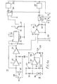
- FIGs 2 and 3 are illustrated the master oscillator circuit and the circuit for the supply of stabilised bias voltages to the rail 27 of oscillator 24 and to the gates of the transistors 36 to 39.
- the circuit of Figure 3 consists of a transformer 49 having parallelled primary windings 50 supplied from an alternating mains source 501.
- a number of secondary windings 51 are provided each of which is connected in series with a full wave diode rectifier 52, the series arrangement of the rectifier 52 and winding 51 being connected in parallel with a smoothing capacitor 53 across which is connected a voltage regulator circuit 54 of known form provided at its input and output sides with decoupling capacitors 55.
- the output sides of the voltage regulators 54 associated with three individual secondary windings 53 provide stable voltages a first of which is supplied across the series path of resistor 56 connected to the gate terminal of transistor 36 and the opto-isolator 44, a second of which is similarly applied to the series path of resistor 57 and opto-isolator 46 of transistor 38, whilst the third is applied both to the series path of resistor 58 and opto-isolator 47 of transistor 39 and to the series path of resistor 59 and opto-isolator 45 of transistor 37.
- a further voltage regulator 54 has the stabilised voltage output thereof applied across rail 27 of oscillator 24 and rail 21 and to various locations of the circuits of Figures 2, 4 and 5.
- the master oscillator 48 of Figure 2 is a free running astable multivibrator, (suitably, digital integrated circuit package RCA Type CD 4047) connected in oscillator mode and including positive feed back capacitor 60.
- the oscillator is provided betwen rails 61 and 62 with a stable voltage from the output side of one of the regulators 54.
- the output side of the oscillator 48 connects via a buffer stage 63 with the mid-point 64 of a chain 65 of components across which chain is supplied a stable voltage from the output side of one of the voltage regulators 54.
- the chain consists of series connected components, namely resistor 66 diodes 67,68,69 and 70 and resistor 71, the mid-point 64 of the chain being the common point of diodes 68 and 69.
- the voltages across diodes 67,68,69 and 70 provide the respective input voltages of the opto-isolators 44,45,46 and 47.
- the output of the oscillator 48 comprises a series of half-cycle pulses so that the circuit affords a precise fifty per cent duty cycle oscillator running at 160 Hertz.
- diodes 67 and 68 are non-conducting whilst diodes 69 and 70 are conducting so that transistors 38 and 39 conduct.
- diodes 67 and 68 conduct whilst diodes 69 and 70 are non-conducting so that transistors 36 and 37 conduct.
- the metal halide arc lamp connected between the terminals 42 and 43 is thus supplied with alternating square wave current pulses of precisely equal duration.
- Figure 5 illustrates a chopper oscillator i.e. oscillator 24, failure detection circuit 74 whilst Figure 4 illustrates a start/stop latch circuit 75, an over-temperature detection circuit 76, a master oscillator failure detection circuit 77, and, a circuit 78 for detecting failure of the stabilised voltage supply circuit of Figure 3.
- a number of power modules 80 each consisting of the circuits contained in the broken lines 3 and 4 of Figure 1 are connected in parallel and the parallel arrangement is connected in series with a relay 82 to the mains - supply.
- the number of parallel connected power modules is governed by the power requirements of the lamp being supplied.
- the relay 84 is energised from the latching circuit 75 which comprises a set/reset bistable latch and consists of two series connected gates 85 and 86. Across the input of gate 85 is a push button switch 87, having in parallel therewith and remote therefrom, a further push button switch 88. The output of gate 86 is fed to a monostable circuit 89 at the output of which is the base of an n-p-n transistor 90 the emitter collector path of which is connected in series with a resistor 91 the voltage across which energises relay 84.
- the gate 86 has a connection to one input of a NOR gate 92 across which is connected the stabilised voltage output of one of the voltage regulators 54.
- the output of the gate 92 is connected to the base of an n-p-n transistor 93, the emitter collector path of which is connected in series with a resistor 94 the voltage across which energises relay 82.
- the stabilised voltage of one of the voltage regulators 54 is connected across the series path of the transistor 93 and resistor 94.
- a second input of the NOR gate is connected to a fail safe busbar 100 to which are connected outputs of the circuits 74,76,77,78.
- buttons 87 or 88 the voltage level at the connection between the gates 86 and 92 goes high so that the level at the output of gate 92 goes low and the contacts of relay 82 open thus depriving the power modules 80 of mains supply so that the lamp is turned off.
- the temperature sensing circuit comprises a comparator 101 to a first input of which is supplied a reference voltage from the common point of resistors 102 and 103 across which is connected the stabilised output voltage of one of the voltage regulators 54.
- resistors 102 and 103 In parallel with resistors 102 and 103 are resistor 99 and series conductor temperature sensor 98,the common point of which is connected to a second input of the comparator.
- the output of the comparator 101 is supplied to the base of an n-p-n transistor 104 the collector-emitter path of which is connected in series with a resistor 105.
- the stabilised voltage output of one of the regulators 54 is supplied tc the comparator and across the series path of the transistor 104 and resistor 105.
- the voltage developed across resistor 105 is supplied by way of a diode 106 to the fail safe busbar 100 connected to an input of the NOR gate 92.
- the reference voltage at the first input of the comparator exceeds the voltage at the second input of the comparator.
- the resistance of the sensor 98 rapidly falls with the result that the voltage at the second input of the comparator rises above the reference voltage.
- An output voltage therefore appears at the comparator which increases conduction of transistor 104 with the result that the voltage across resistor 105 increases and the voltage level at busbar 100 also increases.
- the output voltage level at NOR gate 92 therefore falls and relay 82 opens and interrupts the s ⁇ pply to the power modules 80.
- the master oscillator failure detection circuit 77 consists of a comparator 107 having at one input thereof a reference voltage provided by resistors 108 and 109 the common point of which is connected to the comparator. The other input of the comparator is fed with the output voltage of a peak detection circuit 110 supplied with pulses from the master oscillator. If the master oscillator pulses cease, the output of the peak detection circuit falls below the reference voltage input of the comparator and an output appears at the comparator which renders conducting an n-p-n transistor 111 so that a voltage appears at the busbar 100 which effects opening of the contacts of relay 82. As with the circuits 75 and 76 stabilised voltage supplies to the circuit 77 are provided by the output from one of the voltage regulators 54.
- the chopper oscillator failure detection circuit 74 is connected at points 112 and 113 to corresponding points on the circuit of Figure 1 and is a similar circuit to, though of necessity a much faster operating circuit than, circuit 77. It consists of a peak detection circuit 114 fed at its input 112 with the chopper oscillator frequency. The output of circuit 114 is supplied to one input of a comparator 115 the other input of which is supplied from resistors 116 and 117 with a stable reference voltage.
- the chopper oscillator frequency is a saw tooth waveform which can fail with point 112 at either high or low voltage. If the failure occurs when the voltage at point 112 is low, the condition is safe because transistor 30 is then non-conducting as oscillator 24 is inhibited by the diode 34 and resistor 35. If the oscillator fails when the voltage at point 112 is high, transistor 30 permanently conducts and this condition can lead to destruction of the chopper oscillator and of components of the bridge circuit 2. The circuit 74 prevents such an eventuality and does so in this way. When the oscillator is running, capacitor 120 couples the oscillator voltage to an input of the peak detector circuit 114 and charges capacitor 121.
- Circuit 78 detects failure of the stabilised voltage supply circuit of Figure 3 and comprises a comparator 130 having a reference voltage supplied to one input thereof from a chain of resistors 131 and 132 whilst the other input is supplied with the output voltage of an opto-isolator 123 to the input of which is supplied the stabilised voltage output of one of the voltage regulators 54.
- the reference voltage is higher than this stabilised voltage and to this end the voltage applied to the chain of resistors 121 and 122 is the sum of the stabilised voltage and the voltage applied to opto-isolator 47 of the bridge inverter of Figure 1.
- the output of the comparator 130 is supplied to an opto-isolator 124 the output voltage of which provides the base emitter voltage of an n-p-n transistor 125 the output of which developed across a resistor 126 is connected to the busbar 100 by way of a diode 127.
- the stabilised voltage of one of the voltage regulators is applied to the series path of the collector emitter of transistor 125 and resistor 126.
- each of the circuits 74 and 76 to 78 provides under failure conditions a voltage at the fail safe busbar 100 which is connected to one input of gate 92 and that voltage effects opening of the contacts of relay 82, whilst circuit 75, when it is desired to turn off the lamp connected to the power modules 80, on pressing of switch 87 or 88, supplies a voltage to another input of the gate 92 which likewise effects opening of the contacts of relay 82 thus depriving the lamp of mains power.
- the interruption of the mains supply to the power modules 80 is indicated by illumination of a lamp (not shown) or actuation of some other warning device.
- the constant current source 1 and the inverter bridge circuit 2 as well as the chopper oscillator failure detection circuit 74, are together mounted on a single circuit board of rectangular form to provide one of the power modules 80.
- the board is formed with edge connectors and can be removably engaged along opposite edges thereof in one pair of facing channels or slots in a housing one of the facing channels providing circuit connections complementary with connections on the edge of the circuit board.
- Similar modules 80 can be fitted into further pairs of facing channels in the housing and when so fitted their input connections 8,9 and 10 and their output connections 42 and 43 are automatically connected in parallel with the like connections of other modules 80 engaged in the housing.
- the number of power modules engaged in the housing at any time depends on the power rating of the arc lamp to be illuminated.
- the circuits 75 to 78, the master oscillator circuit of Figure 2 and the power supply circuit of Figure 3 for supplying the stabilised voltages at the various locations mentioned in the circuits of Figures 1,2,4 and 5, are together mounted on a single generally rectangular circuit board which has edge connectors and fits into a pair of facing channels of the housing which accommodates the modules 80. When so fitted the requisite connections are automatically made between the chain 65 of components 66 to 71 of the master oscillator circuit and the inverter bridge circuit 2 of the power modules and between the outputs of the voltage regulators 54 and the appropriate points in the circuits of the power modules.
- the output of the voltage regulator 54 which provides stabilised voltages in the circuits mounted on the protection circuitry circuit board is of course permanently connected to the appropriate points on that board.
Abstract
Description
- This invention relates to power supplies for arc lamps and more particularly to a power supply for a metal halide are lamp such as a mercury, iodine lamp, used to provide daylight and other spectrum lighting, for example, for cinematographic stages, outside television broadcasts and the like.
- Arc lamps of the kind referred to are preferably driven by A.C. since D.C. drive causes rapid erosion of the lamp electrodes. If driven by a sinusoidal current waveform the lamp produces a white light level which is modulated rather than constant as required. This effect arises because, as the supply current passes through zero, the arc gases cool and reheat, the arc being maintained by its thermal inertia, with the result that the light emission from the arc varies. If the lamp is driven by a square current waveform, the speed of passage of the current through zero is greatly increased and modulation of the light output of the arc is greatly reduced.
- It is known to use a power supply for a metal halide arc lamp which consists of a bridge network of switching transistors to provide a square current waveform for driving the arc, the bridge being connected to the supply by way of a series bank of resistors, the supply being either a D.C. generator or a rectified mains supply. Such a power supply is of appreciable bulk primarily because of the size of heat sinks required to dissipate heat generated in the resistor bank and is for that reason expensive to construct. Transportation of the power supply to the location where it is used, moreover, is tedious and expensive.
- The present invention consists in a power supply for an arc lamp, comprising a power source and an inverter, characterised in that the power source is a constant current source for the supply of current to the inverter and the inverter is a bridge network of field effect transistor's and an oscillator adapted to supply square wave voltage switching pulses to the transistors, whereby the bridge network affords an output current of alternating square pulses of current of equal duration for driving the lamp.
- Suitably, the field effect transistors are insulated gate devices supplied with gate to source voltages by way of opto-isolators from the oscillator.
- Preferably, the constant current source comprises an inductor provided with a free wheel diode for connection to a D.C. voltage source and through which current is drawn by a field effect transistor, the current level through which is employed to control the ratio of 'on' to 'off' time of a chopper oscillator supplying the gate to source voltage of the transistor. The current level through the field effect transistor is employed to switch a junction transistor, conduction of which inhibits the oscillator.
- Advantageously, the constant current source and bridge network are mounted on a single circuit board and constitute a power module for parallel connection of the current source input terminals and bridge network output terminals with corresponding terminals of one or more further like power modules. Also with advantage the oscillator for the supply of square voltage switching pulses to the bridge network is mounted as a module on a circuit board which is adapted for connection to the power modules to serve as a common oscillator for the field effect transistor bridge networks thereof. Suitably, the common oscillator module further carries a plurality of system protection circuits, a supply circuit for supplying stabilised voltages to the constant current source, the common oscillator, the bridge network and the protection circuits, and a control circuit adapted upon triggering of any of the protection circuits to disconnect the mains power supply from the power modules.
- The power supply according to the invention represents a considerable saving in weight as compared with the prior art arrangements and is cheaper to construct. It can be used without modification of the electronic circuitry with normally available power sources such as 110
volts 60 cycles per second, and 220volts 50 cycles per second and 120 volts D.C. The modular construction and ability to connect modules in parallel makes the invention readily adaptable for use with lamps of different power. As compared with switching power transistors of the junction type as used in prior arrangements, the use of field effect transistors considerably simplifies the circuitry and enables the modular concept to be implemented with less difficulty than would be the case with bridge circuits employing junction transistors. Junction transistors have considerable disadvantages as compared with field effect transistors when used in an inverter bridge of a power supply. Thus, field effect transistors conduct when a voltage is applied between their gate and source terminals and need only a buffer stage between an oscillator supplying that voltage and the gate and source terminals. Bipolar junction transistors on the other hand require relatively high drive current to bring them into full conduction and further require special protection to guard against secondary breakdown and thermal runaway. The drive circuitry for the field effect transistors is accordingly considerably simplified as compared with that of bipolar transistors and lower switching losses are entailed when field effect transistors are employed. These advantages are achieved moreover with a high power handling capability. - The invention will now be described, by way of example, with reference to the accompanying drawings, in which:-
- FIGURES 1 and 1a are electrical circuit diagrams of a power supply for a metal halide lamp, such as a mercury, iodine lamp;
- FIGURE 2, is a master oscillator circuit for supplying firing pulses to elements of a bridge circuit forming part of Figure 1;
- FIGURE 3, is a circuit for supplying stabilised voltages to various parts of the circuits of Figures 1, 2, 4 and 5; and
- FIGURES 4, 4a and 5 are protection circuits for ensuring fail-safe operation of the circuit of Figure 1 in a variety of circumstances.
- Referring first to Figure 1, the power supply circuit therein illustrated consists of a constant
current source 1 contained in the area enclosed by broken lines 3 and a bridge inverter circuit 2 enclosed by broken lines 4. - The constant
current source 1 consists of a power supply 5 adapted for use with 110 volt or 220 volt, 50 Hertz supplies and to that end comprises two series connected smoothing capacitors 6 and 7 across which the D.C. output voltage of the power supply 5 is developed. Input terminals of the supply 5 comprise live, neutral andearth terminals 8, 9 and 10 respectively, of whichterminal 10 is connected to the casing in which the circuits illustrated in the drawings are accommodated. Live terminal 8 is connected by way of a 220 volt link 11,fuse 12 anddiode 13 to the side of capacitor 6 remote from the common point thereof with capacitor 7 and by way of link 11fuse 12 and diode 14 to the side of capacitor 7 remote from the common point thereof with capacitor 6. To the side of capacitor 6 to whichdiode 13 is connected is also connected adiode 15 which connects with neutral terminal 9 by way of athermistor 17. Adiode 16 is also serially connected by way of thethermistor 17 between terminal 9 and the side of capacitor 7 to which is connected diode 14 and adiode 15 is connected to the common point ofdiode 16 andthermistor 17. Thediodes thermistor 17 has a high resistance at low temperature and thus serves to limit surge currents at start up. - The live terminal 8 is also connected by a 110
volt link 18 and fuse 19 to the common point of capacitors 6 and 7. Thus during one half cycle of the 110 volt supply capacitor 7 is charged viadiode 16 andthermistor 17 and during the next half cycle capacitor 6 is charged by way ofthermistor 17 anddiode 15. Accordingly irrespective of which of thelinks 11 and 18 is in circuit, the series voltage of the output capacitors 6 and 7 is substantially the sum of the fully charged voltages of those capacitors and constitutes the D.C. rectified output voltage provided atrails current source 1. Therails choke 22 through which current can be drawn by afield effect transistor 23 of the insulated gate type. Thetransistor 23 is driven by achopper oscillator 24 which consists ofstages volt voltage rail 27 and positive feedback is afforded bycapacitor 28. The gate to source voltage of thefield effect transistor 23 is supplied from theoscillator 24 by way of abuffer stage 29 and afield effect transistor 30, the latter forming part of the chopper oscillator failure detection circuit hereinafter referred to with reference particularly to Figure 5. - Current drawn by conduction of
field effect transistor 23 throughchoke 22 by way of the load comprising bridge circuit 2 establishes a voltage at the output oftransistor 23 acrossresistor 31 which is sensed at the base ofn-p-n transistor 32 which is connected to the common point ofresistor 31 andtransistor 23 by way of aresistor 33. Thetransistor 32 has its collector to emitter path disposed in series between a series path consisting ofdiode 34 andresistor 35 andlow voltage rail 21 so that whentransistor 32 conducts voltage at the end ofresistor 35 connected withtransistor 32 is reduced and the chopper oscillator is thus inhibited. Accordingly, it will be seen that if excess current is drawn through thechoke 22 by thetransistor 23, a voltage appears acrossresistor 31 which renders that transistor conducting thus inhibiting theoscillator 24 with the result that thetransistor 23 is rendered non-conducting in which state the voltage acrossresistor 31 falls to zero and thetransistor 32 ceases to conduct and the oscillator again supplies the requisite gate to source voltage totransistor 23 for the latter to recommence conduction. In this way the current drawn through thechoke 22 is kept sensibly constant though with a small amount of ripple attributable to the switching frequency of thechopper oscillator 24. This ripple is smoothed bycapacitor 34 and choke 35 at - the input of the circuit 2. The
choke 35 serves to protect the bridge circuit 2 by preventing thecapacitor 34 from discharging intofield effect transistors 36 to 39 forming that bridge circuit and it further serves to protect thechopper oscillator 24 by absorbing voltage spikes when the bridge circuit is initially switched on.Diode 40 is a free-wheel diode which maintains current flow through thechoke 22 whenevertransistor 23 is rendered non-conducting. - The
field effect transistors 36 to 39 are connected in a bridge configuration which at its input side is disposed betweenrails rail 21 includes adiode 41 which allows negative voltage spikes to be absorbed by the main smoothing capacitor 6 and 7.Output terminals alternate pairs output terminals 42 and 43 a square wave alternating output voltage which drives the metal halide lamp load. - The
transistors 36 to 39 are driven at their respective gates via opto-isolators 44 to 47 of a form known per se, each supplied at its input with voltage pulses from amaster oscillator 48 shown in Figure 2. The opto-isolators are essentially devices in which light from a light emitting diode is employed to effect conduction of a photo-transistor, as illustrated, an n-p-n transistor. Successive pulses fromoscillator 48 are supplied respectively to the opto-isolators oftransistor pairs - In Figures 2 and 3 are illustrated the master oscillator circuit and the circuit for the supply of stabilised bias voltages to the
rail 27 ofoscillator 24 and to the gates of thetransistors 36 to 39. The circuit of Figure 3 consists of atransformer 49 having parallelledprimary windings 50 supplied from analternating mains source 501. A number ofsecondary windings 51 are provided each of which is connected in series with a fullwave diode rectifier 52, the series arrangement of therectifier 52 and winding 51 being connected in parallel with asmoothing capacitor 53 across which is connected avoltage regulator circuit 54 of known form provided at its input and output sides withdecoupling capacitors 55. The output sides of thevoltage regulators 54 associated with three individualsecondary windings 53 provide stable voltages a first of which is supplied across the series path ofresistor 56 connected to the gate terminal oftransistor 36 and the opto-isolator 44, a second of which is similarly applied to the series path ofresistor 57 and opto-isolator 46 oftransistor 38, whilst the third is applied both to the series path ofresistor 58 and opto-isolator 47 oftransistor 39 and to the series path ofresistor 59 and opto-isolator 45 oftransistor 37. Afurther voltage regulator 54 has the stabilised voltage output thereof applied acrossrail 27 ofoscillator 24 andrail 21 and to various locations of the circuits of Figures 2, 4 and 5. - The
master oscillator 48 of Figure 2 is a free running astable multivibrator, (suitably, digital integrated circuit package RCA Type CD 4047) connected in oscillator mode and including positive feed backcapacitor 60. The oscillator is providedbetwen rails regulators 54. The output side of theoscillator 48 connects via abuffer stage 63 with the mid-point 64 of achain 65 of components across which chain is supplied a stable voltage from the output side of one of the voltage regulators 54. The chain consists of series connected components, namelyresistor 66diodes resistor 71, the mid-point 64 of the chain being the common point ofdiodes diodes isolators - The output of the
oscillator 48 comprises a series of half-cycle pulses so that the circuit affords a precise fifty per cent duty cycle oscillator running at 160 Hertz. When the output of the master oscillator is high,diodes diodes transistors oscillator 48 is low,diodes diodes transistors terminals - The protection circuitry for the system is illustrated in Figures 4 and 5. Figure 5 illustrates a chopper oscillator i.e.
oscillator 24,failure detection circuit 74 whilst Figure 4 illustrates a start/stop latch circuit 75, anover-temperature detection circuit 76, a master oscillatorfailure detection circuit 77, and, acircuit 78 for detecting failure of the stabilised voltage supply circuit of Figure 3. - In Figure 4 a number of
power modules 80, hereinafter more fully referred to, each consisting of the circuits contained in the broken lines 3 and 4 of Figure 1 are connected in parallel and the parallel arrangement is connected in series with arelay 82 to the mains - supply. The number of parallel connected power modules is governed by the power requirements of the lamp being supplied. - In parallel with the
power modules 80 are connected in series alamp starter 83 andrelay 84. Therelay 84 is energised from the latchingcircuit 75 which comprises a set/reset bistable latch and consists of two series connectedgates gate 85 is apush button switch 87, having in parallel therewith and remote therefrom, a furtherpush button switch 88. The output ofgate 86 is fed to amonostable circuit 89 at the output of which is the base of ann-p-n transistor 90 the emitter collector path of which is connected in series with aresistor 91 the voltage across which energisesrelay 84. Across the series path of thetransistor 90 andresistor 91 and across thegate 85 is connected the stabilised voltage output of one of the voltage regulators 54 (see Figure 3). Thegate 86 has a connection to one input of a NORgate 92 across which is connected the stabilised voltage output of one of the voltage regulators 54. The output of thegate 92 is connected to the base of ann-p-n transistor 93, the emitter collector path of which is connected in series with aresistor 94 the voltage across which energisesrelay 82. The stabilised voltage of one of thevoltage regulators 54 is connected across the series path of thetransistor 93 andresistor 94. A second input of the NOR gate is connected to a failsafe busbar 100 to which are connected outputs of thecircuits - At the commencement of operation both inputs of NOR
gate 92 are low and the output of that gate is therefore high so thatrelay 82 is energised and its contacts are closed. Upon depressingpush button gate 86 is raised - though the voltage at the connection ofgate 86 withgate 92 is taken low - and this triggers themonostable circuit 89 the output voltage level of which goes high for a period which energises thestarter 83 for a period long enough to strike the lamp connected tomodules 80. After the period of the output pulse ofmonostable circuit 89, the output voltage level thereof falls andrelay 84 is de-energised and its contacts are opened. The next time either ofbuttons gates gate 92 goes low and the contacts ofrelay 82 open thus depriving thepower modules 80 of mains supply so that the lamp is turned off. - The temperature sensing circuit comprises a
comparator 101 to a first input of which is supplied a reference voltage from the common point ofresistors resistors resistor 99 and seriesconductor temperature sensor 98,the common point of which is connected to a second input of the comparator. The output of thecomparator 101 is supplied to the base of ann-p-n transistor 104 the collector-emitter path of which is connected in series with aresistor 105. The stabilised voltage output of one of theregulators 54 is supplied tc the comparator and across the series path of thetransistor 104 andresistor 105. The voltage developed acrossresistor 105 is supplied by way of adiode 106 to the failsafe busbar 100 connected to an input of the NORgate 92. - In operation of the temperature sensing circuit the reference voltage at the first input of the comparator, at normal operating temperatures, exceeds the voltage at the second input of the comparator. When howeverlocal temperature rises above a predetermined level, the resistance of the
sensor 98 rapidly falls with the result that the voltage at the second input of the comparator rises above the reference voltage. An output voltage therefore appears at the comparator which increases conduction oftransistor 104 with the result that the voltage acrossresistor 105 increases and the voltage level atbusbar 100 also increases. The output voltage level at NORgate 92 therefore falls andrelay 82 opens and interrupts the sµpply to thepower modules 80. - The master oscillator
failure detection circuit 77 consists of acomparator 107 having at one input thereof a reference voltage provided byresistors peak detection circuit 110 supplied with pulses from the master oscillator. If the master oscillator pulses cease, the output of the peak detection circuit falls below the reference voltage input of the comparator and an output appears at the comparator which renders conducting ann-p-n transistor 111 so that a voltage appears at thebusbar 100 which effects opening of the contacts ofrelay 82. As with thecircuits circuit 77 are provided by the output from one of the voltage regulators 54. - The chopper oscillator
failure detection circuit 74 is connected atpoints circuit 77. It consists of apeak detection circuit 114 fed at itsinput 112 with the chopper oscillator frequency. The output ofcircuit 114 is supplied to one input of acomparator 115 the other input of which is supplied fromresistors - The chopper oscillator frequency is a saw tooth waveform which can fail with
point 112 at either high or low voltage. If the failure occurs when the voltage atpoint 112 is low, the condition is safe becausetransistor 30 is then non-conducting asoscillator 24 is inhibited by thediode 34 andresistor 35. If the oscillator fails when the voltage atpoint 112 is high,transistor 30 permanently conducts and this condition can lead to destruction of the chopper oscillator and of components of the bridge circuit 2. Thecircuit 74 prevents such an eventuality and does so in this way. When the oscillator is running,capacitor 120 couples the oscillator voltage to an input of thepeak detector circuit 114 and charges capacitor 121. When the oscillator fails either in the high or low voltage condition, the voltage at the input ofcircuit 114 to whichcapacitor 120 is connected falls andcapacitor 121 discharges exponentially till it reaches a voltage below the reference voltage at the comparator. The comparator output voltage which was high before discharge ofcapacitor 121 now falls to zero. This output causes a high voltage to appear at the output ofinverter amplifier 118 which forward biases adiode 119 so that a voltage appears at thebusbar 100 and the relay contacts ofrelay 82 are opened. It will be noted that when the output voltage of thecomparator 115 goes low, the voltage atpoint 113 goes low thus ensuring that the gate oftransistor 23 is held low and therefore no current can flow from the mains through thecircuits 1 and 2. -
Circuit 78 detects failure of the stabilised voltage supply circuit of Figure 3 and comprises acomparator 130 having a reference voltage supplied to one input thereof from a chain ofresistors isolator 123 to the input of which is supplied the stabilised voltage output of one of the voltage regulators 54. The reference voltage is higher than this stabilised voltage and to this end the voltage applied to the chain ofresistors 121 and 122 is the sum of the stabilised voltage and the voltage applied to opto-isolator 47 of the bridge inverter of Figure 1. The output of thecomparator 130 is supplied to an opto-isolator 124 the output voltage of which provides the base emitter voltage of ann-p-n transistor 125 the output of which developed across aresistor 126 is connected to thebusbar 100 by way of adiode 127. The stabilised voltage of one of the voltage regulators is applied to the series path of the collector emitter oftransistor 125 andresistor 126. - When the input voltage of the opto-
isolator 123 falls below a predetermined level of about one volt below the nominal stabilised level the output current of the isolator falls and the voltage input from theisolator 123 tocomparator 130 rises above the reference voltage input thereto. The output voltage of the comparator in these circumstances falls so that the output current of opto-isolator 124 falls. This increases conduction oftransistor 127 and the voltage acrossresistor 126 rises and, forward biases thediode 127 so that a voltage is applied tobusbar 100 and the contacts ofrelay 82 open to interrupt the mains supply to thepower modules 80. - It will be apprehended that the heart of the protection circuitry system is the
gate 92. Each of thecircuits safe busbar 100 which is connected to one input ofgate 92 and that voltage effects opening of the contacts ofrelay 82, whilstcircuit 75, when it is desired to turn off the lamp connected to thepower modules 80, on pressing ofswitch gate 92 which likewise effects opening of the contacts ofrelay 82 thus depriving the lamp of mains power. When any of thecircuits 74 to 78 operate to open the contacts ofrelay 82, the interruption of the mains supply to thepower modules 80 is indicated by illumination of a lamp (not shown) or actuation of some other warning device. - The constant
current source 1 and the inverter bridge circuit 2 as well as the chopper oscillatorfailure detection circuit 74, are together mounted on a single circuit board of rectangular form to provide one of thepower modules 80. The board is formed with edge connectors and can be removably engaged along opposite edges thereof in one pair of facing channels or slots in a housing one of the facing channels providing circuit connections complementary with connections on the edge of the circuit board.Similar modules 80 can be fitted into further pairs of facing channels in the housing and when so fitted theirinput connections 8,9 and 10 and theiroutput connections other modules 80 engaged in the housing. The number of power modules engaged in the housing at any time depends on the power rating of the arc lamp to be illuminated. - The
circuits 75 to 78, the master oscillator circuit of Figure 2 and the power supply circuit of Figure 3 for supplying the stabilised voltages at the various locations mentioned in the circuits of Figures 1,2,4 and 5, are together mounted on a single generally rectangular circuit board which has edge connectors and fits into a pair of facing channels of the housing which accommodates themodules 80. When so fitted the requisite connections are automatically made between thechain 65 ofcomponents 66 to 71 of the master oscillator circuit and the inverter bridge circuit 2 of the power modules and between the outputs of thevoltage regulators 54 and the appropriate points in the circuits of the power modules. The output of thevoltage regulator 54 which provides stabilised voltages in the circuits mounted on the protection circuitry circuit board is of course permanently connected to the appropriate points on that board.
Claims (13)
Applications Claiming Priority (2)
| Application Number | Priority Date | Filing Date | Title |
|---|---|---|---|
| GB8123254 | 1981-07-28 | ||
| GB8123254 | 1981-07-28 |
Publications (2)
| Publication Number | Publication Date |
|---|---|
| EP0075382A1 true EP0075382A1 (en) | 1983-03-30 |
| EP0075382B1 EP0075382B1 (en) | 1986-10-08 |
Family
ID=10523556
Family Applications (1)
| Application Number | Title | Priority Date | Filing Date |
|---|---|---|---|
| EP82303612A Expired EP0075382B1 (en) | 1981-07-28 | 1982-07-09 | Power supply for arc lamps |
Country Status (15)
| Country | Link |
|---|---|
| US (1) | US4485434A (en) |
| EP (1) | EP0075382B1 (en) |
| JP (1) | JPS5828197A (en) |
| AR (1) | AR232065A1 (en) |
| AT (1) | ATE22770T1 (en) |
| AU (1) | AU547754B2 (en) |
| BR (1) | BR8204315A (en) |
| CA (1) | CA1185649A (en) |
| DE (1) | DE3273707D1 (en) |
| DK (1) | DK161931B (en) |
| ES (1) | ES514120A0 (en) |
| IN (1) | IN156533B (en) |
| MX (1) | MX154451A (en) |
| NZ (1) | NZ201203A (en) |
| ZA (1) | ZA824856B (en) |
Cited By (3)
| Publication number | Priority date | Publication date | Assignee | Title |
|---|---|---|---|---|
| WO1985001162A1 (en) * | 1983-08-22 | 1985-03-14 | Ncr Corporation | Inverter for uninterruptible power supply |
| EP0361748A1 (en) * | 1988-09-26 | 1990-04-04 | General Electric Company | Power control circuit for discharge lamp and method of operating same |
| DE3925654A1 (en) * | 1989-08-03 | 1991-02-07 | Schmidt Michael | Control unit for discharge lamp(s) - has switches in series connected to DC circuit and diode in parallel in blocking direction |
Families Citing this family (24)
| Publication number | Priority date | Publication date | Assignee | Title |
|---|---|---|---|---|
| AU564304B2 (en) * | 1982-01-15 | 1987-08-06 | Minitronics Pty. Limited | Electronic high frequency controlled device for operating gasdischarge lamps |
| US4682084A (en) * | 1985-08-28 | 1987-07-21 | Innovative Controls, Incorporated | High intensity discharge lamp self-adjusting ballast system sensitive to the radiant energy or heat of the lamp |
| US4649321A (en) * | 1985-10-28 | 1987-03-10 | General Electric Company | Gate capacitance latch for DC to AC converters |
| US4733137A (en) * | 1986-03-14 | 1988-03-22 | Walker Magnetics Group, Inc. | Ion nitriding power supply |
| US4700287A (en) * | 1986-05-30 | 1987-10-13 | Nilssen Ole K | Dual-mode inverter power supply |
| US4779007A (en) * | 1987-02-13 | 1988-10-18 | Unison Technologies, Inc. | Uninterrupted power supply system |
| US4873616A (en) * | 1987-04-16 | 1989-10-10 | Camera Platforms International, Inc. | Power supply for arc lamps |
| US4873617A (en) * | 1987-04-16 | 1989-10-10 | Camera Platforms International, Inc. | Power supply for arc lamps |
| GB2212677B (en) * | 1987-11-16 | 1992-07-22 | Sanyo Electric Co | An electric circuit for supplying controlled frequency electric power to a load |
| US4945467A (en) * | 1988-02-26 | 1990-07-31 | Black & Decker Inc. | Multiple-mode voltage converter |
| DE69033820T2 (en) * | 1989-05-17 | 2002-04-11 | Koninkl Philips Electronics Nv | switching arrangement |
| US5068572A (en) * | 1989-06-08 | 1991-11-26 | U.S. Philips Corporation | Switch mode power supply |
| US4970620A (en) * | 1989-08-23 | 1990-11-13 | General Motors Corporation | FET bridge protection circuit |
| DE4301184C2 (en) * | 1993-01-19 | 1997-12-18 | B & S Elektronische Geraete Gm | Control device for at least one discharge lamp |
| TW339496B (en) * | 1994-06-22 | 1998-09-01 | Philips Electronics Nv | Method and circuit arrangement for operating a high-pressure discharge lamp |
| US7296753B1 (en) * | 2000-01-14 | 2007-11-20 | Bae Systems Information And Electronic Systems Integration Inc. | Isolated control apparatus incorporating light controlled power semiconductors |
| DE10018860A1 (en) | 2000-04-14 | 2001-10-18 | Patent Treuhand Ges Fuer Elektrische Gluehlampen Mbh | Stabilization of the operation of gas discharge lamps |
| US6864642B2 (en) * | 2002-10-07 | 2005-03-08 | Bruce Industries, Inc. | Electronic ballast with DC output flyback converter |
| US6879113B2 (en) * | 2003-03-11 | 2005-04-12 | Bruce Industries, Inc. | Low frequency output electronic ballast |
| EP1649598B1 (en) * | 2003-08-01 | 2008-10-08 | BAE Systems Information and Electronic Warfare Systems | Isolated control apparatus incorporating light controlled power semiconductors |
| JP2008518418A (en) * | 2004-10-29 | 2008-05-29 | コーニンクレッカ フィリップス エレクトロニクス エヌ ヴィ | Strong driver for high intensity discharge lamps |
| KR101100881B1 (en) * | 2004-11-04 | 2012-01-02 | 삼성전자주식회사 | Driving device of light source for display device and display device |
| US7443103B2 (en) | 2005-06-24 | 2008-10-28 | General Electric Company | High pressure lamp with lamp flicker suppression and lamp voltage control |
| US11043951B2 (en) | 2018-11-30 | 2021-06-22 | Palo Alto Research Center Incorporated | Analog computer architecture for fast function optimization |
Citations (1)
| Publication number | Priority date | Publication date | Assignee | Title |
|---|---|---|---|---|
| US4020361A (en) * | 1974-10-04 | 1977-04-26 | Delta Electronic Control Corporation | Switching mode power controller of large dynamic range |
Family Cites Families (10)
| Publication number | Priority date | Publication date | Assignee | Title |
|---|---|---|---|---|
| US3700960A (en) * | 1971-09-23 | 1972-10-24 | Gen Electric | Metal halide lamp system |
| US3737755A (en) * | 1972-03-22 | 1973-06-05 | Bell Telephone Labor Inc | Regulated dc to dc converter with regulated current source driving a nonregulated inverter |
| US3976932A (en) * | 1975-04-15 | 1976-08-24 | General Electric Company | Bridge transistor inverter circuit |
| US3999100A (en) * | 1975-05-19 | 1976-12-21 | Morton B. Leskin | Lamp power supply using a switching regulator and commutator |
| US4042856A (en) * | 1975-10-28 | 1977-08-16 | General Electric Company | Chopper ballast for gaseous discharge lamps with auxiliary capacitor energy storage |
| FR2416617A1 (en) * | 1978-02-07 | 1979-08-31 | Signaux Entr Electriques | CONVERTER FOR THE POWER SUPPLY OF DISCHARGE LAMPS, AND MORE GENERALLY OF ARC LAMPS, AND ITS APPLICATION TO PROJECTORS FOR SUCH LAMPS |
| US4150425A (en) * | 1978-02-09 | 1979-04-17 | Nasa | Module failure isolation circuit for paralleled inverters |
| US4270164A (en) * | 1979-02-28 | 1981-05-26 | Contraves Goerz Corporation | Short circuit protection for switching type power processors |
| JPS55148398A (en) * | 1979-05-09 | 1980-11-18 | Toshiba Corp | X-ray camera |
| JPS55148394A (en) * | 1979-05-10 | 1980-11-18 | Matsushita Electric Works Ltd | Device for firing discharge lamp |
-
1982
- 1982-07-08 ZA ZA824856A patent/ZA824856B/en unknown
- 1982-07-08 NZ NZ201203A patent/NZ201203A/en unknown
- 1982-07-09 DE DE8282303612T patent/DE3273707D1/en not_active Expired
- 1982-07-09 EP EP82303612A patent/EP0075382B1/en not_active Expired
- 1982-07-09 AT AT82303612T patent/ATE22770T1/en not_active IP Right Cessation
- 1982-07-12 US US06/397,596 patent/US4485434A/en not_active Expired - Fee Related
- 1982-07-13 CA CA000407202A patent/CA1185649A/en not_active Expired
- 1982-07-16 AU AU86081/82A patent/AU547754B2/en not_active Ceased
- 1982-07-19 ES ES514120A patent/ES514120A0/en active Granted
- 1982-07-23 BR BR8204315A patent/BR8204315A/en unknown
- 1982-07-23 AR AR290062A patent/AR232065A1/en active
- 1982-07-27 MX MX193769A patent/MX154451A/en unknown
- 1982-07-27 DK DK334482A patent/DK161931B/en not_active Application Discontinuation
- 1982-07-28 JP JP57130546A patent/JPS5828197A/en active Pending
- 1982-07-28 IN IN873/CAL/82A patent/IN156533B/en unknown
Patent Citations (1)
| Publication number | Priority date | Publication date | Assignee | Title |
|---|---|---|---|---|
| US4020361A (en) * | 1974-10-04 | 1977-04-26 | Delta Electronic Control Corporation | Switching mode power controller of large dynamic range |
Non-Patent Citations (1)
| Title |
|---|
| ELECTRONIQUE ET APPLICATIONS INDUSTRIELLES, no. 259, November 1978, pages 19-24, Paris (FR); * |
Cited By (3)
| Publication number | Priority date | Publication date | Assignee | Title |
|---|---|---|---|---|
| WO1985001162A1 (en) * | 1983-08-22 | 1985-03-14 | Ncr Corporation | Inverter for uninterruptible power supply |
| EP0361748A1 (en) * | 1988-09-26 | 1990-04-04 | General Electric Company | Power control circuit for discharge lamp and method of operating same |
| DE3925654A1 (en) * | 1989-08-03 | 1991-02-07 | Schmidt Michael | Control unit for discharge lamp(s) - has switches in series connected to DC circuit and diode in parallel in blocking direction |
Also Published As
| Publication number | Publication date |
|---|---|
| DK334482A (en) | 1983-01-29 |
| MX154451A (en) | 1987-08-27 |
| ES8305550A1 (en) | 1983-04-01 |
| BR8204315A (en) | 1983-07-19 |
| NZ201203A (en) | 1985-08-30 |
| AR232065A1 (en) | 1985-04-30 |
| AU8608182A (en) | 1983-02-03 |
| ES514120A0 (en) | 1983-04-01 |
| DE3273707D1 (en) | 1986-11-13 |
| ATE22770T1 (en) | 1986-10-15 |
| CA1185649A (en) | 1985-04-16 |
| EP0075382B1 (en) | 1986-10-08 |
| AU547754B2 (en) | 1985-10-31 |
| US4485434A (en) | 1984-11-27 |
| JPS5828197A (en) | 1983-02-19 |
| IN156533B (en) | 1985-08-31 |
| ZA824856B (en) | 1983-05-25 |
| DK161931B (en) | 1991-08-26 |
Similar Documents
| Publication | Publication Date | Title |
|---|---|---|
| US4485434A (en) | Power supply for arc lamps | |
| GB2102641A (en) | Power supply for arc lamps | |
| US3626277A (en) | Current regulator suitable for mercury lamp ballast | |
| US4135223A (en) | Electronic protection circuit | |
| US4213164A (en) | Electronic protection circuit incorporating voltage divider sensing, gating and triggering | |
| GB2031623A (en) | Power supplies | |
| JPS6139850A (en) | Circuit device for monitoring thyristor | |
| SU1184056A1 (en) | Voltage converter | |
| SU1661897A1 (en) | Device for motor overheat protection | |
| SU1432652A1 (en) | Device for protecting three-phase induction motor from two-phase operation and braked-rotor duty | |
| SU1490299A1 (en) | Group power source with spark-proof outputs | |
| SU892433A2 (en) | Dc voltage stabilizer with overload protection | |
| SU1365300A1 (en) | A.c. to d.c. voltage converter | |
| JPH0628949Y2 (en) | Gate turn-off thyristor gate power supply circuit | |
| SU1567797A1 (en) | Spark-proof power-supply source | |
| SU1555759A1 (en) | Automatic switch for protection of load from connection to ac power supply source with intolerable rated voltage | |
| GB2248984A (en) | An emergency light circuit | |
| SU1584025A1 (en) | Combination device for protecting of electrical installation from damage under emergency conditions of operation | |
| KR880002944Y1 (en) | A preventive circuit of electric shock | |
| SU1108585A1 (en) | A.c. voltage-to-d.c. voltage converter | |
| SU482105A1 (en) | Sparkproof power supply source | |
| SU1376279A1 (en) | Lighting device | |
| SU586527A1 (en) | Device for discharging dc source | |
| SU1029330A2 (en) | Remote control device with zero protection | |
| SU1626368A1 (en) | Key element |
Legal Events
| Date | Code | Title | Description |
|---|---|---|---|
| PUAI | Public reference made under article 153(3) epc to a published international application that has entered the european phase |
Free format text: ORIGINAL CODE: 0009012 |
|
| AK | Designated contracting states |
Designated state(s): AT BE CH DE FR GB IT LI LU NL SE |
|
| 17P | Request for examination filed |
Effective date: 19830916 |
|
| GRAA | (expected) grant |
Free format text: ORIGINAL CODE: 0009210 |
|
| AK | Designated contracting states |
Kind code of ref document: B1 Designated state(s): AT BE CH DE FR GB IT LI LU NL SE |
|
| REF | Corresponds to: |
Ref document number: 22770 Country of ref document: AT Date of ref document: 19861015 Kind code of ref document: T |
|
| ET | Fr: translation filed | ||
| ITF | It: translation for a ep patent filed |
Owner name: ING. A. GIAMBROCONO & C. S.R.L. |
|
| REF | Corresponds to: |
Ref document number: 3273707 Country of ref document: DE Date of ref document: 19861113 |
|
| PLBI | Opposition filed |
Free format text: ORIGINAL CODE: 0009260 |
|
| PG25 | Lapsed in a contracting state [announced via postgrant information from national office to epo] |
Ref country code: LU Free format text: LAPSE BECAUSE OF NON-PAYMENT OF DUE FEES Effective date: 19870731 |
|
| 26 | Opposition filed |
Opponent name: B & S ELEKTRONISCHE GERAETE GMBH Effective date: 19870701 |
|
| NLR1 | Nl: opposition has been filed with the epo |
Opponent name: B & S ELEKTRONISCHE GERAETE GMBH |
|
| REG | Reference to a national code |
Ref country code: GB Ref legal event code: 732 |
|
| REG | Reference to a national code |
Ref country code: GB Ref legal event code: 732 |
|
| ITTA | It: last paid annual fee | ||
| PGFP | Annual fee paid to national office [announced via postgrant information from national office to epo] |
Ref country code: NL Payment date: 19900731 Year of fee payment: 9 |
|
| PGFP | Annual fee paid to national office [announced via postgrant information from national office to epo] |
Ref country code: GB Payment date: 19900816 Year of fee payment: 9 |
|
| PGFP | Annual fee paid to national office [announced via postgrant information from national office to epo] |
Ref country code: SE Payment date: 19900822 Year of fee payment: 9 Ref country code: LU Payment date: 19900822 Year of fee payment: 9 |
|
| PGFP | Annual fee paid to national office [announced via postgrant information from national office to epo] |
Ref country code: FR Payment date: 19900829 Year of fee payment: 9 Ref country code: BE Payment date: 19900829 Year of fee payment: 9 |
|
| PGFP | Annual fee paid to national office [announced via postgrant information from national office to epo] |
Ref country code: CH Payment date: 19900830 Year of fee payment: 9 |
|
| PGFP | Annual fee paid to national office [announced via postgrant information from national office to epo] |
Ref country code: DE Payment date: 19900831 Year of fee payment: 9 Ref country code: AT Payment date: 19900831 Year of fee payment: 9 |
|
| PG25 | Lapsed in a contracting state [announced via postgrant information from national office to epo] |
Ref country code: GB Effective date: 19910709 Ref country code: AT Effective date: 19910709 |
|
| PG25 | Lapsed in a contracting state [announced via postgrant information from national office to epo] |
Ref country code: SE Effective date: 19910710 |
|
| PG25 | Lapsed in a contracting state [announced via postgrant information from national office to epo] |
Ref country code: LI Free format text: LAPSE BECAUSE OF NON-PAYMENT OF DUE FEES Effective date: 19910731 Ref country code: CH Free format text: LAPSE BECAUSE OF NON-PAYMENT OF DUE FEES Effective date: 19910731 Ref country code: BE Effective date: 19910731 |
|
| BERE | Be: lapsed |
Owner name: LEE ELECTRIC (LIGHTING) LTD Effective date: 19910731 |
|
| PG25 | Lapsed in a contracting state [announced via postgrant information from national office to epo] |
Ref country code: NL Effective date: 19920201 |
|
| GBPC | Gb: european patent ceased through non-payment of renewal fee | ||
| NLV4 | Nl: lapsed or anulled due to non-payment of the annual fee | ||
| PG25 | Lapsed in a contracting state [announced via postgrant information from national office to epo] |
Ref country code: FR Effective date: 19920331 |
|
| REG | Reference to a national code |
Ref country code: CH Ref legal event code: PL |
|
| PG25 | Lapsed in a contracting state [announced via postgrant information from national office to epo] |
Ref country code: DE Effective date: 19920401 |
|
| REG | Reference to a national code |
Ref country code: FR Ref legal event code: ST |
|
| RDAG | Patent revoked |
Free format text: ORIGINAL CODE: 0009271 |
|
| STAA | Information on the status of an ep patent application or granted ep patent |
Free format text: STATUS: PATENT REVOKED |
|
| 27W | Patent revoked |
Effective date: 19920622 |
|
| EUG | Se: european patent has lapsed |
Ref document number: 82303612.4 Effective date: 19920210 |