EP0073620A2 - FM counter detector - Google Patents
FM counter detector Download PDFInfo
- Publication number
- EP0073620A2 EP0073620A2 EP82304416A EP82304416A EP0073620A2 EP 0073620 A2 EP0073620 A2 EP 0073620A2 EP 82304416 A EP82304416 A EP 82304416A EP 82304416 A EP82304416 A EP 82304416A EP 0073620 A2 EP0073620 A2 EP 0073620A2
- Authority
- EP
- European Patent Office
- Prior art keywords
- signal
- frequency
- coupled
- difference
- sound
- Prior art date
- Legal status (The legal status is an assumption and is not a legal conclusion. Google has not performed a legal analysis and makes no representation as to the accuracy of the status listed.)
- Withdrawn
Links
- 230000005236 sound signal Effects 0.000 claims description 21
- 230000007704 transition Effects 0.000 claims description 8
- 238000012935 Averaging Methods 0.000 claims description 5
- 238000001514 detection method Methods 0.000 abstract description 6
- 239000003990 capacitor Substances 0.000 description 6
- 238000010586 diagram Methods 0.000 description 4
- 238000000034 method Methods 0.000 description 3
- 230000000694 effects Effects 0.000 description 2
- 238000013459 approach Methods 0.000 description 1
- 230000002238 attenuated effect Effects 0.000 description 1
- 239000000919 ceramic Substances 0.000 description 1
- 238000010276 construction Methods 0.000 description 1
- 238000011084 recovery Methods 0.000 description 1
- 238000000926 separation method Methods 0.000 description 1
- 239000007787 solid Substances 0.000 description 1
- 238000001228 spectrum Methods 0.000 description 1
Images

Classifications
-
- H—ELECTRICITY
- H03—ELECTRONIC CIRCUITRY
- H03D—DEMODULATION OR TRANSFERENCE OF MODULATION FROM ONE CARRIER TO ANOTHER
- H03D3/00—Demodulation of angle-, frequency- or phase- modulated oscillations
- H03D3/02—Demodulation of angle-, frequency- or phase- modulated oscillations by detecting phase difference between two signals obtained from input signal
- H03D3/04—Demodulation of angle-, frequency- or phase- modulated oscillations by detecting phase difference between two signals obtained from input signal by counting or integrating cycles of oscillations
-
- H—ELECTRICITY
- H04—ELECTRIC COMMUNICATION TECHNIQUE
- H04N—PICTORIAL COMMUNICATION, e.g. TELEVISION
- H04N5/00—Details of television systems
- H04N5/44—Receiver circuitry for the reception of television signals according to analogue transmission standards
- H04N5/60—Receiver circuitry for the reception of television signals according to analogue transmission standards for the sound signals
- H04N5/62—Intercarrier circuits, i.e. heterodyning sound and vision carriers
Definitions
- This invention relates to angle modulation detectors and, in particular, to a frequency modulation counter detection system useful in television receiver apparatus.
- United States Patent number 3,399,353 describes an-FM counter-type detector arrangement in which a frequency modulated carrier signal is applied to an oscillator circuit which, in the absence of the applied signal, generates self-oscillations at'a frequency which is harmonically related to the center or unmodulated frequency of the carrier signal.
- the circuit locks in frequency and phase with the applied signal to provide an output signal at a frequency related to the frequency of the applied signal.
- the oscillator output signal is used to develop a pulse signal, including constant area pulses, at a rate related to the frequency of the FM carrier signal. The pulse signal is then averaged to derive the original modulation information.
- the FM counter-type detector system described above is especially attractive for consumer oriented products, such as television receivers, because the counter type detector is constructed without tuned circuit elements, such as those necessary for a conventional FM discriminator.
- the counter detector thus readily lends itself to construction in integrated circuit form.
- the use of a counter-type detector results in a very linear demodulation process, as compared to a discriminator relying upon the relatively nonlinear characteristics of a conventional tuned circuit.
- the counter-type detector produces a relatively low level detected signal.
- the signal level can be increased, but a maximum ratio is quickly attained at which the duration of the constant area pulse approaches the duration of one period of the highest instantaneous modulated carrier frequency. Even at this maximum mark-to-space ratio, the detected signal level is normally relatively low. Accordingly, it is desirable to increase the demodulated signal level of the counter detector.
- a counter-type detector system for a television receiver in which the angle modulated intermediate frequency signal is heterodyned to a lower frequency prior to detection by the counter detector.
- the lower intermediate frequency permits the generation of a pulse signal which is averaged to produce a relatively high level detected output signal.
- additional selectivity may be used prior to detection to further attenuate signal frequencies above the lower carrier frequency.
- a counter detector system is emplyed in the sound channel of a television receiver.
- the conventional sound i.f. signal is heterodyned with the television color subcarrier to produce a second sound i.f. signal at the difference frequency of these two signals.
- the second sound i.f. signal is further filtered prior to detection by the counter detector, which produces a relatively high level output signal as a result of the heterodyning process.
- the principles of the present invention are employed in a SECAM color signal demodulator.
- the frequency-modulated SECAM color signals are heterodyned with the sound carrier in a SECAM television receiver to produce FM color signals at lower frequencies.
- the color signal information is then recovered by a single counter-type detector.
- a television second detector 10 produces baseband video and intercarrier sound signals at its output. These signals are applied to the input of an intercarrier sound trap and take-off circuit 12, which may for example be constructed as shown in United States Patent Application Serial Number 085,312 filed October 26, 1979, and entitled "SIGNAL SEPARATION NETWORKS".
- This circuit operates to separate the intercarrier sound and video signals.
- the video signal including a color burst component, is applied to video signal processing circuits 44, which process the video signal for display of the video information on a television kinescope (not shown).
- the intercarrier sound signal is applied to the input of an intercarrier sound bandpass filter 16.
- the color burst signal component has a frequency of approximately 3.58 MHz
- the intercarrier sound signal, or sound i.f. signal comprises audio information frequency modulated on a 4.5 MHz carrier.
- the intercarrier sound signal bandpass filter 16 passes signals in the vicinity of the intercarrier sound signal frequency.
- This filter has a center or resonant frequency equal to the intercarrier sound signal carrier (e.g., 4.5 MHz) and may comprise, for example, a ceramic filter.
- the filtered intercarrier sound signal is then amplified and limited by an amplifier-limiter stage 18, and the amplified and limited signal is applied to one input of a mixer 20.
- the second input of the mixer 20 is coupled to receive a color subcarrier signal from the video signal processing circuits 44, which include a conventicnal automatic frequency and phase control cirouit for producing a phase-locked color subcarrier signal is response to the color burst signal component.
- the color suboaurier signal is also used to demodulate color signals in the video signal processing circuits in the normal manner.
- the miner 20 heterodynes the intercarrier sound signal of nominally 4.5 MHz with the color subcarrier signal of 3.58 MHz to produce a difference signal of 920 KHz, frequency modulated by audio information.
- This difference signal is filtered by a lowpass filter 22 to attenuate signals of frequencies above the frequency of the modulated 920 KHz signal.
- the second sound i.f. signal is amplified and limited by an amplifier-limiter 24 and applied to the input of a monostable multivibrator 30, which produces a train of constant width pulses in response to transitions of the second sound i.f. signal of a given sense (i.e., positive-going transitions or negative-going transitions).
- the train of constant width pulses is averaged to recover the audio information and the recovered audio signal is deemphasized by an integrator and deemphasis circuit 32.
- the audio signal is applied to an audio amplifier 40 and a loudspeaker 42 for reproduction of the audio information.
- FIGURE 3 a typical pulse train produced by the monostable multivibrator 30 from two modulating frequencies is shown.
- the pulse train At a low modulating frequency f 2 , the pulse train has a cycle of T 1 duration, including a fixed duration pulse M and a space S 1 .
- the pulse train At a high modulating frequency f l , the pulse train has a cycle of T 2 duration, including the fixed duration pulse M and the shorter space S 2 .
- the pulse train has a constant amplitude, E.
- the recovered audio signal will have an average energy content of: which, for the high and low modulating frequencies is equal to
- This function is seen to be linear, and is proportional to the voltage supply which determines E, the frequency deviation f 2 -f l , and the width of the pulses M.
- the width of the pulses M cannot exceed the period T 2 of the highest instantaneous frequency during frequency modulation for recovery of the audio information.
- the pulse width M is bounded by zero and 1/(f c +f 2 -f 1/ 2) microseconds, where f c is the carrier frequency.
- the duration of the M pulse can be increased in the ratio of 4500/920, or 14 dB.
- the audio output is increased by 14 dB by the use of the second sound i.f. signal.
- the mixer 20 comprises a commercially available CA3072 chroma demodulator integrated circuit coupled to perform the mixing function.
- Pin 8 of the integrated circuit is coupled to a source of supply voltage (B+), and pin 14 is coupled to a source of reference potential (ground).
- Bias voltage circuits internal to the integrated circuit develop bias voltages V b1 and V b2 .
- the mixing function is performed by doubly balanced modulators including amplifier sections 72A and 72B, and switching sections 76A and 76B, which receive current from current sources 74A and 74B.
- the intercarrier sound signal produced by the amplifier-limiter 18 is supplied by way of an input terminal 3 to the left sides of the amplifier sections 72A and 72B.
- the intercarrier sound signal is also coupled by way of a series resistor 62, a shunt capacitor 64, and an input terminal 4 to the right sides of the amplifier sections.
- the amplifier sections provide amplified intercarrier sound signals to the emitter-coupled switching sections 76A and 76B.
- the color subcarrier signal from the video signal processing circuits 14 is applied by way of an emitter-follower coupled transistor 70 and an input terminal 7 to one side of the switching sections 76A and 76B.
- the other side of the switching sections is coupled to signal reference potential by an input terminal 6 and a capacitor 66.
- the difference signal produced at the outputs of the switching section is coupled by way of a lowpass filter output stage 78 to an output terminal 13.
- a potentiometer 80 is coupled between output terminal 13 and ground, and is used as a gain-determinirg control element.
- the intercarrier sound second i.f. signal is taken from the wiper arm of the potentiometer 80 and applied to the input of an active lowpass filter 22, including an emitter-follower coupled transistor 82 and a capacitor 84.
- the filter 22 rolls off signals of frequencies above approximately 1.5 MHz to reduce the effects of impulse noise on the sound system.
- the filtered 920 KHz signal is coupled by way of amplifier-limiter 24 to an input terminal 1 of a 74123 type monostable multivibrator integrated circuit.
- Pins 2, 3 and 16 of the 74123 integrated circuit are coupled to the B+ supply, and pin 8 of the integrated circuit is coupled to ground.
- a time constant circuit 90 including a resistor 96, a potentiometer 94, and a capacitor 92 is coupled to pins 16, 15 and 14 of the 74123 integrated circuit to determine the duration of the pulses produced by the circuit.
- the time constant circuit 90 is adjusted to produce pulses of approximately .85 microsecond duration.
- the resultant pulse train at the output terminal 4 thus has a very high duty cycle, or mark-to-space ratio. Since the modulated 920 KHz signal can have cycles varying between approximately 1.058 and 1.117 microseconds, the duty cycle of the pulse train will vary between seventy-six and eighty percent.
- the pulse train produced by the monostable multivibrator 30 is averaged by an integrating circuit 100, including a series coupled resistor 102 and a shunt coupled capacitor 104 to recover the audio information.
- the audio signal then undergoes conventional FM deemphasis in a deemphasis network 110, including a series-coupled resistor 112 and a shunt-coupled capacitor 114.
- the audio signal is applied to the base of an emitter follower coupled output transistor 116, to produce an audio output signal at an output terminal 118.
- a source of SECAM television signals 200 produces frequency modulated chrominance'subcarriers D OB and D OR at approximately 4.25 and 4.4 MHz, and an amplitude modulated sound carrier 250 at 6.5 MHz, as shown in the frequency spectrum plot of FIGURE 5a.
- These signals are applied to a chroma bandpass filter 202, which produces the filtered chrominance subcarrier signals at its output, and to a sound carrier take-off circuit 204, which produces the modulated sound carrier at its output.
- the chrominance subcarrier signals at the output of the filter 202 are filtered by a highpass filter 208, amplified by an amplifier 210, filtered by a further highpass filter 212, and applied to the input of a mixer circuit 214.
- the modulated sound carrier at the output of the circuit 204 is applied to sound demodulating circuitry (not shown) and to an amplifier-limiter 206.
- the amplified and limited sound carrier at the output of the amplifier-limiter 206 is applied to a second input of the mixer 214.
- the mixer 214 produces difference signals by intermodulating the chrominance subcarrier signals and the sound carrier signal.
- the chrominance subcarrier difference signals are developed at approximately 2.1 and 2.25 MHz as shown by subcarrier D'OR and D' 0B in FIGURE 5b. Signals above these frequencies are attenuated by a lowpass filter 216 and the chrominance subcarrier signals are further amplified by an amplifier 218, then filtered again by a lowpass filter 220.
- the chrominance subcarrier signals are amplified and limited by an amplifier-limiter 224 and applied to a monostable multivibrator 230, which produces constant width pulses in response to transitions of the amplified and limited.chrominance subcarrier signals.
- the widths of these pulses are again set to be slightly less than the period of the highest instantaneous frequency of the modulated subcarrier signals.
- the pulse train produced by the monostable multivibrator 230 is averaged by an averaging circuit 232 to recover the color information and the color signals are deemphasized by a deemphasis circuit 240.
- the color signals are then applied to chroma signal processing circuitry (not shown) for further-processing.
- the SECAM chrominance subcarrier signals D OB and D OR are transmitted on alternate lines of the video signal, and the counter detector is perfectly linear, only a single detector (monostable multivibrator 230 and averaging circuit 232) is required to demodulate both signals. Demodulation at the lower carrier intermediate frequencies increases the levels of the recovered color signals as compared with demodulation at their higher intermediate frequencies, and also permits the use of lowpass filters 216 and 220 for additional selectivity and improved performance in the presence of noise.
- the CA3072 Chroma Demodulator integrated circuit mentioned earlier is available from the Solid State Division of the present applicants and further information about it is contained in their Data Book SSD-240A, Linear Integrated Circuits (1978).
- the 74123 integrated circuit is a standard type of monostable multivibrator available from many makers such as Motorola (USA) and Ferranti (UK).
Abstract
In counter-type detector system suitable for a television receiver a standard angle modulated frequency signal is heterodyned (20) to a lower frequency prior to detection by the counter detector (30, 32). The lower intermediate frequency permits the generation of a pulse signal which is averaged to produce a relatively high level detected output signal. After the angle modulated frequency signal has been converted to the lower frequency, additional selectivity (22, 24) may be used prior to detection to further attenuate signal frequencies above the lower carrier frequency.
Description
- This invention relates to angle modulation detectors and, in particular, to a frequency modulation counter detection system useful in television receiver apparatus.
- United States Patent number 3,399,353 describes an-FM counter-type detector arrangement in which a frequency modulated carrier signal is applied to an oscillator circuit which, in the absence of the applied signal, generates self-oscillations at'a frequency which is harmonically related to the center or unmodulated frequency of the carrier signal. When the carrier signal is applied to the oscillator circuit, the circuit locks in frequency and phase with the applied signal to provide an output signal at a frequency related to the frequency of the applied signal. The oscillator output signal is used to develop a pulse signal, including constant area pulses, at a rate related to the frequency of the FM carrier signal. The pulse signal is then averaged to derive the original modulation information.
- The FM counter-type detector system described above is especially attractive for consumer oriented products, such as television receivers, because the counter type detector is constructed without tuned circuit elements, such as those necessary for a conventional FM discriminator. The counter detector thus readily lends itself to construction in integrated circuit form. In addition, the use of a counter-type detector results in a very linear demodulation process, as compared to a discriminator relying upon the relatively nonlinear characteristics of a conventional tuned circuit.
- It has been found that the counter-type detector produces a relatively low level detected signal. By increasing the mark-to-space ratio, or duty cycle, of the pulse signal which is averaged to recover the modulating information, the signal level can be increased, but a maximum ratio is quickly attained at which the duration of the constant area pulse approaches the duration of one period of the highest instantaneous modulated carrier frequency. Even at this maximum mark-to-space ratio, the detected signal level is normally relatively low. Accordingly, it is desirable to increase the demodulated signal level of the counter detector.
- In accordance with the principles of the present invention, a counter-type detector system is provided for a television receiver in which the angle modulated intermediate frequency signal is heterodyned to a lower frequency prior to detection by the counter detector. The lower intermediate frequency permits the generation of a pulse signal which is averaged to produce a relatively high level detected output signal. After the angle modulated intermediate frequency signal has been converted to the lower frequency, additional selectivity may be used prior to detection to further attenuate signal frequencies above the lower carrier frequency.
- In a first embodiment of the present invention, a counter detector system is emplyed in the sound channel of a television receiver. The conventional sound i.f. signal is heterodyned with the television color subcarrier to produce a second sound i.f. signal at the difference frequency of these two signals. The second sound i.f. signal is further filtered prior to detection by the counter detector, which produces a relatively high level output signal as a result of the heterodyning process.
- In a second embodiment of the present invention, the principles of the present invention are employed in a SECAM color signal demodulator. The frequency-modulated SECAM color signals are heterodyned with the sound carrier in a SECAM television receiver to produce FM color signals at lower frequencies. The color signal information is then recovered by a single counter-type detector.
- In the drawings:
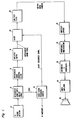
- FIGURE 1 illustrates, in block diagram form, a counter-type detector system in the sound channel of a television receiver constructed in accordance with the principles of the present invention;
- FIGURE 2 illustrates, partially in block diagram form and partially in schematic diagram form, a more detailed embodiment of the system of FIGURE 1;
- FIGURE 3 illustrates a pulse signal used to explain the operation of the embodiments of FIGURES 1 and 2;
- FIGURE 4 illustrates a SECAM color signal detector constructed in accordance with the principles of the present invention; and
- FIGURES 5a and 5b illustrate the frequency location of certain signals used to explain the operation of the embodiment of FIGURE 4.
- Referring to FIGURE 1, a television sound channel constructed in accordance with the principles of the present invention is shown. A television
second detector 10 produces baseband video and intercarrier sound signals at its output. These signals are applied to the input of an intercarrier sound trap and take-offcircuit 12, which may for example be constructed as shown in United States Patent Application Serial Number 085,312 filed October 26, 1979, and entitled "SIGNAL SEPARATION NETWORKS". This circuit operates to separate the intercarrier sound and video signals. The video signal, including a color burst component, is applied to videosignal processing circuits 44, which process the video signal for display of the video information on a television kinescope (not shown). The intercarrier sound signal is applied to the input of an intercarriersound bandpass filter 16. In the United States NTSC system, the color burst signal component has a frequency of approximately 3.58 MHz, and the intercarrier sound signal, or sound i.f. signal, comprises audio information frequency modulated on a 4.5 MHz carrier. - The intercarrier sound
signal bandpass filter 16 passes signals in the vicinity of the intercarrier sound signal frequency. This filter has a center or resonant frequency equal to the intercarrier sound signal carrier (e.g., 4.5 MHz) and may comprise, for example, a ceramic filter. The filtered intercarrier sound signal is then amplified and limited by an amplifier-limiter stage 18, and the amplified and limited signal is applied to one input of amixer 20. The second input of themixer 20 is coupled to receive a color subcarrier signal from the videosignal processing circuits 44, which include a conventicnal automatic frequency and phase control cirouit for producing a phase-locked color subcarrier signal is response to the color burst signal component. The color suboaurier signal is also used to demodulate color signals in the video signal processing circuits in the normal manner. - The
miner 20 heterodynes the intercarrier sound signal of nominally 4.5 MHz with the color subcarrier signal of 3.58 MHz to produce a difference signal of 920 KHz, frequency modulated by audio information. - This difference signal, the second sound i.f. signal, is filtered by a
lowpass filter 22 to attenuate signals of frequencies above the frequency of the modulated 920 KHz signal. The second sound i.f. signal is amplified and limited by an amplifier-limiter 24 and applied to the input of amonostable multivibrator 30, which produces a train of constant width pulses in response to transitions of the second sound i.f. signal of a given sense (i.e., positive-going transitions or negative-going transitions). The train of constant width pulses is averaged to recover the audio information and the recovered audio signal is deemphasized by an integrator anddeemphasis circuit 32. The audio signal is applied to anaudio amplifier 40 and aloudspeaker 42 for reproduction of the audio information. - The effect of the generation of the second sound i.f. signal is seen by referring to the pulse train diagram of FIGURE 3. Referring to FIGURE 3, a typical pulse train produced by the
monostable multivibrator 30 from two modulating frequencies is shown. At a low modulating frequency f2, the pulse train has a cycle of T1 duration, including a fixed duration pulse M and a space S1. At a high modulating frequency fl, the pulse train has a cycle of T2 duration, including the fixed duration pulse M and the shorter space S2. The pulse train has a constant amplitude, E. When the pulse train is averaged bycircuit 100, the recovered audio signal will have an average energy content of:

- This function is seen to be linear, and is proportional to the voltage supply which determines E, the frequency deviation f2-fl, and the width of the pulses M. The width of the pulses M cannot exceed the period T2 of the highest instantaneous frequency during frequency modulation for recovery of the audio information. Thus, the pulse width M is bounded by zero and 1/(fc+f2-f1/2) microseconds, where fc is the carrier frequency. When the carrier frequency is changed from 4.5 MHz to 920 KHz, the duration of the M pulse can be increased in the ratio of 4500/920, or 14 dB. Thus, the audio output is increased by 14 dB by the use of the second sound i.f. signal.
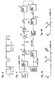
- The arrangement of FIGURE 1 is shown in further detail in FIGURE 2. In this embodiment, the
mixer 20 comprises a commercially available CA3072 chroma demodulator integrated circuit coupled to perform the mixing function.Pin 8 of the integrated circuit is coupled to a source of supply voltage (B+), andpin 14 is coupled to a source of reference potential (ground). Bias voltage circuits internal to the integrated circuit (not shown) develop bias voltages Vb1 and Vb2. The mixing function is performed by doubly balanced modulators includingamplifier sections 72A and 72B, and switchingsections 76A and 76B, which receive current fromcurrent sources - The intercarrier sound signal produced by the amplifier-
limiter 18 is supplied by way of aninput terminal 3 to the left sides of theamplifier sections 72A and 72B. The intercarrier sound signal is also coupled by way of aseries resistor 62, ashunt capacitor 64, and aninput terminal 4 to the right sides of the amplifier sections. The amplifier sections provide amplified intercarrier sound signals to the emitter-coupledswitching sections 76A and 76B. - The color subcarrier signal from the video
signal processing circuits 14 is applied by way of an emitter-follower coupledtransistor 70 and an input terminal 7 to one side of the switchingsections 76A and 76B. The other side of the switching sections is coupled to signal reference potential by aninput terminal 6 and acapacitor 66. The difference signal produced at the outputs of the switching section is coupled by way of a lowpassfilter output stage 78 to anoutput terminal 13. - A
potentiometer 80 is coupled betweenoutput terminal 13 and ground, and is used as a gain-determinirg control element. The intercarrier sound second i.f. signal is taken from the wiper arm of thepotentiometer 80 and applied to the input of anactive lowpass filter 22, including an emitter-follower coupledtransistor 82 and acapacitor 84. Thefilter 22 rolls off signals of frequencies above approximately 1.5 MHz to reduce the effects of impulse noise on the sound system. The filtered 920 KHz signal is coupled by way of amplifier-limiter 24 to aninput terminal 1 of a 74123 type monostable multivibrator integrated circuit. -
Pins pin 8 of the integrated circuit is coupled to ground. A timeconstant circuit 90, including aresistor 96, apotentiometer 94, and acapacitor 92 is coupled topins constant circuit 90 is adjusted to produce pulses of approximately .85 microsecond duration. The resultant pulse train at theoutput terminal 4 thus has a very high duty cycle, or mark-to-space ratio. Since the modulated 920 KHz signal can have cycles varying between approximately 1.058 and 1.117 microseconds, the duty cycle of the pulse train will vary between seventy-six and eighty percent. - The pulse train produced by the
monostable multivibrator 30 is averaged by an integratingcircuit 100, including a series coupledresistor 102 and a shunt coupledcapacitor 104 to recover the audio information. The audio signal then undergoes conventional FM deemphasis in adeemphasis network 110, including a series-coupledresistor 112 and a shunt-coupled capacitor 114. The audio signal is applied to the base of an emitter follower coupledoutput transistor 116, to produce an audio output signal at anoutput terminal 118. - The principles of the present invention may also be applied to a SECAM system color demodulator, as shown in the embodiment of FIGURE 4. A source of SECAM television signals 200 produces frequency modulated chrominance'subcarriers DOB and DOR at approximately 4.25 and 4.4 MHz, and an amplitude modulated
sound carrier 250 at 6.5 MHz, as shown in the frequency spectrum plot of FIGURE 5a. These signals are applied to achroma bandpass filter 202, which produces the filtered chrominance subcarrier signals at its output, and to a sound carrier take-off circuit 204, which produces the modulated sound carrier at its output. The chrominance subcarrier signals at the output of thefilter 202 are filtered by ahighpass filter 208, amplified by anamplifier 210, filtered by a furtherhighpass filter 212, and applied to the input of amixer circuit 214. The modulated sound carrier at the output of thecircuit 204 is applied to sound demodulating circuitry (not shown) and to an amplifier-limiter 206. The amplified and limited sound carrier at the output of the amplifier-limiter 206 is applied to a second input of themixer 214. - The
mixer 214 produces difference signals by intermodulating the chrominance subcarrier signals and the sound carrier signal. The chrominance subcarrier difference signals are developed at approximately 2.1 and 2.25 MHz as shown by subcarrier D'OR and D'0B in FIGURE 5b. Signals above these frequencies are attenuated by alowpass filter 216 and the chrominance subcarrier signals are further amplified by anamplifier 218, then filtered again by alowpass filter 220. The chrominance subcarrier signals are amplified and limited by an amplifier-limiter 224 and applied to amonostable multivibrator 230, which produces constant width pulses in response to transitions of the amplified and limited.chrominance subcarrier signals. The widths of these pulses are again set to be slightly less than the period of the highest instantaneous frequency of the modulated subcarrier signals. The pulse train produced by themonostable multivibrator 230 is averaged by an averagingcircuit 232 to recover the color information and the color signals are deemphasized by adeemphasis circuit 240. The color signals are then applied to chroma signal processing circuitry (not shown) for further-processing. - Since the SECAM chrominance subcarrier signals DOB and DOR are transmitted on alternate lines of the video signal, and the counter detector is perfectly linear, only a single detector (
monostable multivibrator 230 and averaging circuit 232) is required to demodulate both signals. Demodulation at the lower carrier intermediate frequencies increases the levels of the recovered color signals as compared with demodulation at their higher intermediate frequencies, and also permits the use oflowpass filters - The CA3072 Chroma Demodulator integrated circuit mentioned earlier is available from the Solid State Division of the present applicants and further information about it is contained in their Data Book SSD-240A, Linear Integrated Circuits (1978). The 74123 integrated circuit is a standard type of monostable multivibrator available from many makers such as Motorola (USA) and Ferranti (UK).
Claims (11)
1. In receiver apparatus which includes a source (10,200) of signals having an angle modulated carrier signal and a second signal of a substantially constant frequency, a counter detector demodulation system which comprises:
pulse generating means (30,230) responsive to an angle modulated signal derived from said carrier signal for producing a train of constant width pulses in response to transitions of said derived angle modulated signal; and
an averaging circuit (32,232) coupled to receive said constant width pulses for recovering information angle modulated on said derived signal and passing said recovered information to a utilization circuit (42); and which is characterised by:
means (44,206) for providing from said second signal a reference signal of said substantially constant frequency; and
a mixer (20,214) having a first input coupled to receive said angle modulated carrier signal, a second input coupled to receive said reference signal, and an output at which an angle modulated difference signal is produced, the pulse generating means (30) being responsive to this difference signal.
2. Apparatus as claimed in Claim 1 which is a television receiver apparatus wherein said source (10,200) is a source of baseband television signals.
3. Apparatus as claimed in Claim 2, wherein:
said source of baseband signals includes a detector (lO) which produces an intercarrier sound signal and a baseband video signal, said second signal including a color burst signal component of a given frequency;
said reference signal providing means (44) is responsive to said color burst signal component for producing a continuous wave signal at said given frequency;
said mixer (20) has a first input coupled to receive said intercarrier sound signal, a second input coupled to receive said continuous wave signal, and an output at which a difference frequency signal, frequency modulated by sound information, is produced;
said pulse generating means (30) is responsive to said difference frequency signal for producing said train of constant width pulses in response to transitions of said difference frequency signal; and
said averaging circuit (32) is coupled to receive these constant width pulse train to produce a recovered sound signal which is supplied to a sound signal utilization circuit (24,42).
4. Apparatus as claimed in Claim 3, wherein a bandpass filter (16) is coupled between said detector (10) and said first input of said mixer (20) for passing said intercarrier sound signal.
5. Apparatus as claimed in Claim 3 or 4 wherein said means for producing said continuous wave signal includes a color subcarrier automatic phase control loop circuit.
6. Apparatus as claimed in Claim 2, wherein:
said television receiver is a SECAM television receiver;
said source (200) produces frequency modulated chrominance subcarrier signals and a sound carrier signal of a given frequency;
said reference signal providing means (206) is responsive to said sound carrier signal for producing a continuous wave reference signal at said given frequency;
said mixer (214) has a first input coupled to receive said chrominance subcarrier signals, a second input coupled to receive said reference signals, and an output at which a difference frequency signal, frequency modulated with chrominance information, is produced;
said pulse generating means (230) is responsive to said difference frequency signal for producing a train of constant width pulses in response to transitions of said difference frequency signal; and
said averaging circuit (240) is coupled to receive said constant width pulse train for producing recovered chrominance information signals which are supplied to chrominance signal utilization circuitry.
7. Apparatus as claimed in Claim 6, wherein said means for providing a reference signal includes an amplifier-limiter circuit (206).
8. Apparatus as claimed in any preceding Claim wherein a lowpass filter (22,216), coupled between said mixer (20,214) and said pulse generating means (30,230), has a response characteristic for attenuating frequencies above the frequency of said difference signal.
9. Apparatus as claimed in Claim 8, wherein an amplifier-limiter circuit (24,224) is coupled between said mixer and said pulse generating means for producing a limited replica of said difference signal.
10. Apparatus as claimed in any preceding Claim wherein said pulse generating means is a monostable multivibrator (30) responsive to transitions of said difference signal of a given polarity for producing a train of pulses having constant widths which are less than the period of the highest frequency of said difference signal.
11. Apparatus as claimed in any preceding Claim wherein said utilization circuit includes a deemphasis circuit (32,240).
Applications Claiming Priority (2)
| Application Number | Priority Date | Filing Date | Title |
|---|---|---|---|
| US297555 | 1981-08-31 | ||
| US06/297,555 US4395735A (en) | 1981-08-31 | 1981-08-31 | FM Counter detector |
Publications (2)
| Publication Number | Publication Date |
|---|---|
| EP0073620A2 true EP0073620A2 (en) | 1983-03-09 |
| EP0073620A3 EP0073620A3 (en) | 1984-08-15 |
Family
ID=23146812
Family Applications (1)
| Application Number | Title | Priority Date | Filing Date |
|---|---|---|---|
| EP82304416A Withdrawn EP0073620A3 (en) | 1981-08-31 | 1982-08-20 | Fm counter detector |
Country Status (3)
| Country | Link |
|---|---|
| US (1) | US4395735A (en) |
| EP (1) | EP0073620A3 (en) |
| JP (1) | JPS5850805A (en) |
Families Citing this family (4)
| Publication number | Priority date | Publication date | Assignee | Title |
|---|---|---|---|---|
| NL8200328A (en) * | 1982-01-29 | 1983-08-16 | Philips Nv | TV-MF SWITCHING. |
| US4843334A (en) * | 1986-12-09 | 1989-06-27 | Canon Kabushiki Kaisha | Frequency demodulator operable with low frequency modulation carriers |
| JPH03103703U (en) * | 1990-02-09 | 1991-10-28 | ||
| JPH04252679A (en) * | 1991-01-29 | 1992-09-08 | Matsushita Electric Ind Co Ltd | Television receiver |
Citations (5)
| Publication number | Priority date | Publication date | Assignee | Title |
|---|---|---|---|---|
| US2750441A (en) * | 1951-09-06 | 1956-06-12 | Motorola Inc | Intercarrier sound system |
| US3399353A (en) * | 1967-06-02 | 1968-08-27 | Rca Corp | Fm counter-type detector especially suited for integrated circuit fabrication |
| GB1163330A (en) * | 1965-12-31 | 1969-09-04 | Int Standard Electric Corp | Receiver for Frequency-Modulated Signals |
| JPS5567256A (en) * | 1978-11-14 | 1980-05-21 | Trio Kenwood Corp | Fm stereo tuner |
| GB2062386A (en) * | 1979-10-26 | 1981-05-20 | Rca Corp | Intercarrier sound separation networks |
Family Cites Families (1)
| Publication number | Priority date | Publication date | Assignee | Title |
|---|---|---|---|---|
| NL7712887A (en) * | 1977-11-23 | 1979-05-28 | Philips Nv | TELEVISION RECEIVER WITH AN ADJUSTABLE NOISE CANCELLATION FILTER. |
-
1981
- 1981-08-31 US US06/297,555 patent/US4395735A/en not_active Expired - Fee Related
-
1982
- 1982-08-20 EP EP82304416A patent/EP0073620A3/en not_active Withdrawn
- 1982-08-30 JP JP57151642A patent/JPS5850805A/en active Pending
Patent Citations (5)
| Publication number | Priority date | Publication date | Assignee | Title |
|---|---|---|---|---|
| US2750441A (en) * | 1951-09-06 | 1956-06-12 | Motorola Inc | Intercarrier sound system |
| GB1163330A (en) * | 1965-12-31 | 1969-09-04 | Int Standard Electric Corp | Receiver for Frequency-Modulated Signals |
| US3399353A (en) * | 1967-06-02 | 1968-08-27 | Rca Corp | Fm counter-type detector especially suited for integrated circuit fabrication |
| JPS5567256A (en) * | 1978-11-14 | 1980-05-21 | Trio Kenwood Corp | Fm stereo tuner |
| GB2062386A (en) * | 1979-10-26 | 1981-05-20 | Rca Corp | Intercarrier sound separation networks |
Non-Patent Citations (2)
| Title |
|---|
| L'ONDE ELECTRIQUE, vol. 56, no. 4, April 1976, pages 200-203, Paris, FR; Z. HAJOS: "Un nouveau démodulateur SECAM à comptage d'impulsions réalisé en technologie TTl" * |
| PATENTS ABSTRACTS OF JAPAN, vol. 4, no. 109, 6th August 1980, page E-20, 591; & JP-A-55 067 256 (TRIO) (CAT. X) 21-05-1980 * |
Also Published As
| Publication number | Publication date |
|---|---|
| EP0073620A3 (en) | 1984-08-15 |
| JPS5850805A (en) | 1983-03-25 |
| US4395735A (en) | 1983-07-26 |
Similar Documents
| Publication | Publication Date | Title |
|---|---|---|
| CA1269442A (en) | Agc in sound channel of system for processing a scrambled video signal | |
| US4353093A (en) | Impulse noise reduction system for TV receivers | |
| US5526062A (en) | Color TV receiver using quadrature-phase synchronous detector for supplying signal to chrominance circuitry | |
| US4167749A (en) | Noise reduction apparatus | |
| US3794754A (en) | Pal-type color signal processing apparatus | |
| US4511924A (en) | Frequency translation phase-locked loop for separate or intercarrier type television sound detection | |
| US4395735A (en) | FM Counter detector | |
| EP0003169B1 (en) | Secam-pal television signal converter and receiver including said converter | |
| US4470070A (en) | Frequency translation phase-locked loop television sound detection system | |
| US4148058A (en) | PAL switching control circuit | |
| CA1219064A (en) | Hybrid frequency modulation feedback loop remote volume control circuit | |
| US4513323A (en) | Buzz reduction for intercarrier type television sound detection | |
| US3812289A (en) | Television receiver using synchronous video detection | |
| CA1101987A (en) | Synchronous detector particularly adapted for a video if signal | |
| US4072983A (en) | SECAM identification circuit | |
| US4660088A (en) | Quasi-parallel television if suitable for stereo sound reception | |
| US3961135A (en) | Synchronized demodulation system | |
| NL8200368A (en) | TELEVISION SOUND RECEIVER. | |
| KR920002840B1 (en) | Tv sound detection system | |
| Rzeszewski | A system approach to synchronous detection | |
| JPS60194609A (en) | Television receiver | |
| US5206908A (en) | Method and apparatus for detecting timing pulses for scrambled television system | |
| CA1212464A (en) | Television sound detection system using a frequency translation phase-locked loop | |
| JPH0424666Y2 (en) | ||
| KR930001829B1 (en) | Circuit for removing noise |
Legal Events
| Date | Code | Title | Description |
|---|---|---|---|
| PUAI | Public reference made under article 153(3) epc to a published international application that has entered the european phase |
Free format text: ORIGINAL CODE: 0009012 |
|
| AK | Designated contracting states |
Designated state(s): DE FR GB IT |
|
| PUAL | Search report despatched |
Free format text: ORIGINAL CODE: 0009013 |
|
| AK | Designated contracting states |
Designated state(s): DE FR GB IT |
|
| STAA | Information on the status of an ep patent application or granted ep patent |
Free format text: STATUS: THE APPLICATION IS DEEMED TO BE WITHDRAWN |
|
| 18D | Application deemed to be withdrawn |
Effective date: 19850301 |
|
| RIN1 | Information on inventor provided before grant (corrected) |
Inventor name: HOLMES, DAVID DUNLAP |