EP0072921B1 - Method and equipment for the mounting of electrical terminal boards - Google Patents
Method and equipment for the mounting of electrical terminal boards Download PDFInfo
- Publication number
- EP0072921B1 EP0072921B1 EP82106460A EP82106460A EP0072921B1 EP 0072921 B1 EP0072921 B1 EP 0072921B1 EP 82106460 A EP82106460 A EP 82106460A EP 82106460 A EP82106460 A EP 82106460A EP 0072921 B1 EP0072921 B1 EP 0072921B1
- Authority
- EP
- European Patent Office
- Prior art keywords
- contact elements
- contact
- pressing
- openings
- pin
- Prior art date
- Legal status (The legal status is an assumption and is not a legal conclusion. Google has not performed a legal analysis and makes no representation as to the accuracy of the status listed.)
- Expired
Links
Images


Classifications
-
- H—ELECTRICITY
- H01—ELECTRIC ELEMENTS
- H01R—ELECTRICALLY-CONDUCTIVE CONNECTIONS; STRUCTURAL ASSOCIATIONS OF A PLURALITY OF MUTUALLY-INSULATED ELECTRICAL CONNECTING ELEMENTS; COUPLING DEVICES; CURRENT COLLECTORS
- H01R43/00—Apparatus or processes specially adapted for manufacturing, assembling, maintaining, or repairing of line connectors or current collectors or for joining electric conductors
- H01R43/20—Apparatus or processes specially adapted for manufacturing, assembling, maintaining, or repairing of line connectors or current collectors or for joining electric conductors for assembling or disassembling contact members with insulating base, case or sleeve
- H01R43/205—Apparatus or processes specially adapted for manufacturing, assembling, maintaining, or repairing of line connectors or current collectors or for joining electric conductors for assembling or disassembling contact members with insulating base, case or sleeve with a panel or printed circuit board
-
- H—ELECTRICITY
- H05—ELECTRIC TECHNIQUES NOT OTHERWISE PROVIDED FOR
- H05K—PRINTED CIRCUITS; CASINGS OR CONSTRUCTIONAL DETAILS OF ELECTRIC APPARATUS; MANUFACTURE OF ASSEMBLAGES OF ELECTRICAL COMPONENTS
- H05K13/00—Apparatus or processes specially adapted for manufacturing or adjusting assemblages of electric components
- H05K13/04—Mounting of components, e.g. of leadless components
-
- Y—GENERAL TAGGING OF NEW TECHNOLOGICAL DEVELOPMENTS; GENERAL TAGGING OF CROSS-SECTIONAL TECHNOLOGIES SPANNING OVER SEVERAL SECTIONS OF THE IPC; TECHNICAL SUBJECTS COVERED BY FORMER USPC CROSS-REFERENCE ART COLLECTIONS [XRACs] AND DIGESTS
- Y10—TECHNICAL SUBJECTS COVERED BY FORMER USPC
- Y10T—TECHNICAL SUBJECTS COVERED BY FORMER US CLASSIFICATION
- Y10T29/00—Metal working
- Y10T29/49—Method of mechanical manufacture
- Y10T29/49002—Electrical device making
- Y10T29/49117—Conductor or circuit manufacturing
- Y10T29/49124—On flat or curved insulated base, e.g., printed circuit, etc.
- Y10T29/49147—Assembling terminal to base
- Y10T29/49151—Assembling terminal to base by deforming or shaping
- Y10T29/49153—Assembling terminal to base by deforming or shaping with shaping or forcing terminal into base aperture
-
- Y—GENERAL TAGGING OF NEW TECHNOLOGICAL DEVELOPMENTS; GENERAL TAGGING OF CROSS-SECTIONAL TECHNOLOGIES SPANNING OVER SEVERAL SECTIONS OF THE IPC; TECHNICAL SUBJECTS COVERED BY FORMER USPC CROSS-REFERENCE ART COLLECTIONS [XRACs] AND DIGESTS
- Y10—TECHNICAL SUBJECTS COVERED BY FORMER USPC
- Y10T—TECHNICAL SUBJECTS COVERED BY FORMER US CLASSIFICATION
- Y10T29/00—Metal working
- Y10T29/53—Means to assemble or disassemble
- Y10T29/5313—Means to assemble electrical device
- Y10T29/53174—Means to fasten electrical component to wiring board, base, or substrate
Definitions
- the invention refers to a method and to an apparatus for mounting elongated electrical connectors on a sheet element, for example a circuit board, wherein the sheet element has openings for receiving and holding contact elements of the electrical connectors.
- the invention refers in particular to a method and to an apparatus for mounting electric pin connectors, comprising a pin connector body adapted to support contact elements, on a sheet element, for example a circuit board, having openings adapted to receive said contact elements; said contact elements have, preferably, the shape of a pin; each pin comprises at one end a contact pin (knife contact) and at the other end a termination section; a press-fit section is provided between said contact pin and said termination section.
- the contact elements are preferably arranged in the form of a strip (contact element comb) and can be pressed simultaneously into the respective openings of the sheet element.
- a method is already known according to which a plurality of contact springs is arranged together in the form of a strip; thereupon said contact springs are inserted into openings of a circuit board until wider portions, which serve as press-fit portions, come into engagement with the edges of said openings.
- ribs thereof come into engagement with said strip.
- the wider portions are pressed into the openings, which are plated with a conductive material.
- a strip comprising a plurality of said contact elements is inserted into a pressing tool, in order to subsequently press the contact elements into the openings of a circuit board by means of said pressing tool.
- This method requires the use of a suitable hole matrix (i.e.-support plate provided with holes), in order to accommodate the leading ends of the contact elements while the press-fit portions are pressed into the openings of the circuit board.
- a pilot strip after removal of a pilot strip the additional step of mounting the connector body is necessary. Consequently, not only an expensive support plate with holes must be used as support plate for the circuit board, but also a relatively large number of method steps is necessary.
- US-A-4 127 935 relates to a method for assembly of electrical connectors.
- contacts are inserted into an insulator, an insulator which is first supported on the upper surface of a back-up board so that each sleeve of the insulator is positioned above and in vertical alignment with relatively large clearance holes in the board.
- an insulator having rows of contacts lightly supported in the sleeves thereof is positioned above a printed circuit board with the tail portions of each of the contacts being received with clearance into aligned circular mounting apertures in said circuit board.
- a seating tool the contacts are moved downwardly through the sleeves and press fit the shank portions of the contacts into the apertures in the printed circuit board. It is noted that this method requires a back-up board and two steps to complete the connector.
- US-A-3 769 679 relates to an apparatus for manufacturing connector terminals.
- This apparatus requires a backing plate having a plurality of guide holes drilled therethrough and a number of upstanding alignment pins is mounted along the edge.
- a circuit board into which terminals are to be inserted is placed upon the surface of the backing plate.
- contact terminals are shown which are joined by a support strip. After the contacts have been press fit into the circuit board, the support strip is no longer needed and is removed. This is done by a braking tool.
- the method set forth in the precharacterizing part of claim 1 is characterized by the features of the characterizing part of claim 1.
- a pressing tool as set forth in the precharacterizing part of claim 3, a tool which is characterized by the features of the characterizing part of claim 3.
- this invention provides an insulating connector body for use in the method of claim 1, said insulating connector body being characterized in that cams are provided adjacent to slots for forming a support surface with their upper sides.
- the pressing tool of the invention which generally can be used with any method for providing press-fit contacts, has the advantage that the pilot strip which connects the individual contact elements is cleanly and practically automatically removed without requiring an additional tool.
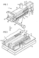
- Fig. 2 and Fig. 16d elongated connectors 10, in particular connectors having contact pins (pin connectors) and are efficiently mounted on a printed circuit board 8. None of the figures shows the pin connector 10 completely mounted on a circuit board 8. However, the front part of Fig. 2 and also Fig. 16d gives a clear picture of a pin connector in its final mounting position.
- Fig. 2 as well as Fig. 16d shows pin contact elements 5 having wire wrap post sections 13 (yet to be described in more detail) projecting upwards while contact pins 12 extend into a pin connector body 11. Said contact pins 12 are adapted to receive, after removal of the circuit board 8 from a support plate 60, socket- type contact elements of a connector equipped therewith.
- the use of the pressing tool 1 shown in Fig. 1 makes it possible to press a pin contact element comb 2 into the circuit board 8 and simultaneously into a pin connector body 11. (Pressing direction 9 in Fig. 1, 2.)
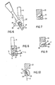
- Fig. 1 as well as Figs. 3-10 disclose a pressing tool 1 designed according to the invention.
- This pressing tool 1 is adapted to receive and hold a series of pin contact elements 5, which have to be inserted by means of a pressing operation into a circuit board 8 (shown especially in Fig. 2 and Fig. 16) as well as into a pin connector body (insulation body or connector body) which is used for supporting the circuit board 8 during the pressing operation.
- pin contact elements 5 are used even though the use of contact elements in general is contemplated.
- the pin contact elements 5 are provided preferably in the form of a pin contact element comb 2, in the case of which the individual pin contact elements 5 are connected by a pilot strip 6; said pilot strip 6 can be severed by the pressing tool 1 according to the invention without requiring the use of an additional tool.
- the pressing tool 1 comprises a frame section of portion 30 in the center of which a holding section 4 is provided in order to allow the mounting of the pressing tool 1 in, for example, a hand press (not shown).
- the clamping section of portion 3 is pivotally mounted in the frame portion 30 and serves for holding a contact element comb, especially in a pin contact element comb 2 in the receiving position shown in Fig. 8.
- the frame portion 30 comprises an L-shaped elongated portion 33 with side walls 31, 32, with the clamping portion 3 being arranged in the area of the recess of the "L" (see for example Fig. 8).
- the clamping portion 3 comprises a first clamping element (holder) 34 and a second clamping element (flap) 35.
- the holder 34 and the flap 35 are pivotally mounted on a bolt 36 fastened in side wall 31 and on a bolt 37 fastened in side wall 32.
- the holder 34 has a length somewhat longer than the length of the pin contact comb 2 to be received in clamping portion 3. Normally, that is to say in the receiving position of the clamping portion 3, the holder 34 assumes the position shown in Figs.
- a torsion spring 136 which (see Fig. 8) acts in counterclockwise direction.
- the side walls of the holder 34 which are not designated by reference numerals, limit the pivotal movement in counterclockwise direction by abutting at frame portion 30 as shown in Fig. 3.
- Guide teeth 39 are arranged over the entire length of holder 34 so as to guide the individual pin contact elements 5 of the pin contact comb 2 into their proper positions in the clamping portion 3.
- a rubber strip 52 extends behind the guide teeth 39; said rubber strip 52 is inserted into the upper side of holder 34 and is adapted to come into contact with the contact elements 5. Alternatively, the rubber strip can be inserted into the bottom side of flap 35.
- the pivotable flap 35 is connected in a non- rotatable manner with bolt 37 by means of a pin 38.
- the bolt 37 (see specifically Fig. 4) extends beyond the side wall 32 and supports a lever 53.
- Lever 53 is connected with bolt 37 by means of a pivot element 40.
- the pivot element 40 is pivotable about pin 41 which extends through pivot element 40 and bolt 37.
- Pivot element 40 is kept in the position shown in Fig. 4 by means of a compression spring 42.
- An abutment element 43 is provided on the pivot element 40 diametrically opposite to the fastening position of lever 53. Abutment element 43 comprises detent surface 44.
- the detent surface 44 is adapted to cooperate with an abutment surface 46 of a detent means 45 of the side wall 32 in the manner shown in Fig. 1.
- the spring 42 holds the pivot element 40 in the position shown in Fig. 1.
- a bevel 47 (see Fig. 4) permits the pivotal movement of lever 53 in lengthwise direction of the frame portion 30 so as to allow a movement out of the rest position shown in Fig. 1.
- Front surfaces 54 of adjacent teeth 39 (see Fig. 3) of the holder 34 form contact surfaces for the press-fit sections 14 of the pin contact elements 5.
- the front surfaces 54 limit the insertion of the pin contact element comb 2 into the clamping portion 3 such that the individual contact elements 5 are aligned uniformly and are arranged with their intended severing portions 49 under an elongated edge 50 (Fig. 10) of the elongated portion 33.
- the front surfaces 54 are used to transmit the pressing force to the individual contact elements 5 at the time the pressing operation is carried out.
- the pilot strip 6 of the contact elements 5 is arranged under a counter pressure surface 51 formed by clamping portion 3 (Fig. 8) provided that the contact element comb 2 is properly inserted into its mounting or receiving position. Surface 51 takes up the pressure of the holder 34 during the press-in operation.
- FIG. 1 and 16 *Mounting or support plate 60 (Fig. 1 and 16) is used with the method and apparatus of the invention for supporting the circuit board 8.
- Mounting plate 60 is generally somewhat larger than the circuit board 8 which has to be equipped with pin connector bodies 11.
- the pin connector bodies 11 to be mounted on the circuit board 8 are arranged (see Fig. 2) with a desired distance from each other on the mounting plate 60.
- the pin connector bodies support the circuit board 8.
- Fig. 16a shows bore holes 61 in the mounting plate 60 on both sides so as to receive mounting and centering pins 62 (Fig. 2 and 16).
- the pin connector bodies 11 are arranged with their diametrically provided fastening openings 70 (Fig. 11) on the mounting pins 62.
- Openings 80 (Fig. 2, 16) provided on opposite sides in the circuit board 8, again arranged with a predetermined distance, permit the insertion of the circuit board 8 onto the mounting pins 62 in a supporting relationship with the pin connector bodies 11.
- openings 7 plated with an electrically conductive material are provided in the circuit board. These openings 7 are best to be recognized in Figs. 16c and 16d.
- the openings 7 are then found in alignment with corresponding slots (openings) 90 (Fig. 11) of the pin connector bodies 11.
- a pin connector body 11 with, for example, three rows a, b, c of slots as shown in Fig. 11, three rows of openings 7 are provided in the circuit board 8 in corresponding positions.
- the openings 7 are not shown in Fig. 2.
- the circuit board 8 consists generally of an insulating material and the contact elements 5 are intended to be pressed into the above-mentioned openings 7.
- a simple circuit board or even a circuit board of the so-called stacked design can be used with the invention.
- the circuit board can support electric components and can be a printed circuit board.
- the circuit board can also be a back plane circuit board. Instead of using the expression "circuit board”, one can more generally refer to a "receiving element for elongate connectors" or to a "sheet element".
- Fig. 1 schematically shows a pin contact element comb 2
- Fig. 13 shows a small section of it, namely, two pin contact elements 5 connected with each other by pilot strip 6.
- Each pin contact element 5 comprises a press-fit section 14 in its middle area and arranged at opposite ends a pin contact or contact pin 12 (in general terms a contact section) and a wire wrap post section 13b (in general terms a termination section).
- each pin contact element 5 is connected via its wire wrap post section 13 with pilot strip 6, and the contact section 12 is a contact pin or knife contact.
- the presence of intended severing portions 49 between the termination section 13 - preferably the wire wrap post sections - and the pilot strip 6 facilitates the separation of the pilot strip 6.
- the pin or plug connector body 11 (insulating body) according to the invention is shown especially in Figs. 11 and 12 as well as in Fig. 16. Since, preferably, a pin connector body 11 is used according to the invention and is also shown in the drawing, the latter expression will be used in the following description.
- the pin connector body 11 is made of a plastic material and comprises a pin connector body wall section 15 and a pin connector body base section 16.
- the wall section 15 is formed by two parallel walls which form a pin connector body space 19 which is open at its two narrow sides.
- the already mentioned fastening openings 70 are formed diametrically opposite to each other.
- the base section 16 is penetrated by a plurality of slots 90, already mentioned, which extend between a bottom side 17 and an inner-upper side 92.
- the slots 90 can be arranged in the rows a, b, c (see Fig. 11) already mentioned. For example, 32 slots (or more or less) can be arranged in each row a, b, c.
- the bottom side 17 of the pin connector body 11 is not plane but exhibits cams 93, 94 adjacent to the slots 90. These cams are shown only for the rows 1, 2 and 3 in Fig. 11.
- grooves 95 extend in a lengthwise direction between each two rows of slots 90.
- Ledges 96 are formed by grooves 97 on both sides of the pin connector body 11 and extend around the fastening openings 70.
- the ledges 96 are of the same height as the cams 93, 94.
- the pin connector body 11 thus forms a smooth but interrupted support surface with its bottom side 17 (which is directed upward in Fig. 2 and 16) for the circuit board 8 so that air may escape when bottom side 17 contacts the circuit board 8. So as to form cams 93, 94, grooves 98 extend transversely to grooves 95.
- the pin connector bodies 11 are arranged at the desired locations on centering pins 62 which were already inserted in mounting plate 60.
- the pin connector bodies 11 contact with their upper side 18 the mounting plate 60.
- the circuit board 8 is arranged on the centering pins 62 and comes into contact with the bottom side 17 of the pin connector bodies 11 which are provided with the cams 93 and 94. The just described procedure assures that the openings 7 in the circuit board 8 are aligned with the slots 90 in the pin connector bodies 11.
- the mounting plate 60 is now mounted on the table of a press (not shown) in alignment with the press-in tool 1 arranged in the upper part of the press.
- the pin contact element comb 2 of the type shown in Fig. 13 is inserted into the pressing tool 1 such that the pin contact element comb 2 lies with its abutment surfaces of the press-fit sections 14 at the front surfaces 54 of teeth 39 (see Fig. 3).
- the movable flap 35 is moved by about 30° by means of lever 53 until the pin contact element comb 2 is firmly clamped in clamping portion 3.
- the holder 34 provides a counterpressure support due to the action of the compression spring 136.
- the entire pressing tool 1 is moved downwardly so as to press the pin contact elements (with the pin sections first) to a certain degree into the aligned openings 7 of the circuit board 8, while at the same time, the insertion of the pin contact elements into the pin connector bodies 11, which are arranged below the circuit board 8, occurs.
- the flap 35 is opened by moving the lever 53 against the force exerted by compression spring 42, the severed pilot strip 6 is released and drops.
- the pilot strip 6 can be guided into a box over a chute.
- another pin contact element comb 2 can be pressed into circuit board. Similar operations are continued until all the desired contact elements are inserted.
Description
- The invention refers to a method and to an apparatus for mounting elongated electrical connectors on a sheet element, for example a circuit board, wherein the sheet element has openings for receiving and holding contact elements of the electrical connectors.
- The invention refers in particular to a method and to an apparatus for mounting electric pin connectors, comprising a pin connector body adapted to support contact elements, on a sheet element, for example a circuit board, having openings adapted to receive said contact elements; said contact elements have, preferably, the shape of a pin; each pin comprises at one end a contact pin (knife contact) and at the other end a termination section; a press-fit section is provided between said contact pin and said termination section. The contact elements are preferably arranged in the form of a strip (contact element comb) and can be pressed simultaneously into the respective openings of the sheet element.
- A method is already known according to which a plurality of contact springs is arranged together in the form of a strip; thereupon said contact springs are inserted into openings of a circuit board until wider portions, which serve as press-fit portions, come into engagement with the edges of said openings. When mounting a connector body, ribs thereof come into engagement with said strip. By pressing on the upper side of said body, e.g. by means of a stem of a press, the wider portions are pressed into the openings, which are plated with a conductive material. With this known method, it is disadvantageous, among other things, that a counter support plate must be provided for each connector body; said support plate has to be provided with holes for accommodating the wire wrap posts.
- According to another known method for mounting press-fit contact elements, a strip comprising a plurality of said contact elements is inserted into a pressing tool, in order to subsequently press the contact elements into the openings of a circuit board by means of said pressing tool. This method requires the use of a suitable hole matrix (i.e.-support plate provided with holes), in order to accommodate the leading ends of the contact elements while the press-fit portions are pressed into the openings of the circuit board. Furthermore, after removal of a pilot strip the additional step of mounting the connector body is necessary. Consequently, not only an expensive support plate with holes must be used as support plate for the circuit board, but also a relatively large number of method steps is necessary.
- US-A-4 127 935 relates to a method for assembly of electrical connectors. In accordance with this method contacts are inserted into an insulator, an insulator which is first supported on the upper surface of a back-up board so that each sleeve of the insulator is positioned above and in vertical alignment with relatively large clearance holes in the board. Thereupon, an insulator having rows of contacts lightly supported in the sleeves thereof, is positioned above a printed circuit board with the tail portions of each of the contacts being received with clearance into aligned circular mounting apertures in said circuit board. By means of a seating tool the contacts are moved downwardly through the sleeves and press fit the shank portions of the contacts into the apertures in the printed circuit board. It is noted that this method requires a back-up board and two steps to complete the connector.
- US-A-3 769 679 relates to an apparatus for manufacturing connector terminals. This apparatus requires a backing plate having a plurality of guide holes drilled therethrough and a number of upstanding alignment pins is mounted along the edge. A circuit board into which terminals are to be inserted is placed upon the surface of the backing plate. Also, contact terminals are shown which are joined by a support strip. After the contacts have been press fit into the circuit board, the support strip is no longer needed and is removed. This is done by a braking tool.
- In accordance with this invention, the method set forth in the precharacterizing part of
claim 1 is characterized by the features of the characterizing part ofclaim 1. - Also in accordance with this invention, there is provided a pressing tool as set forth in the precharacterizing part of
claim 3, a tool which is characterized by the features of the characterizing part ofclaim 3. - In addition, this invention provides an insulating connector body for use in the method of
claim 1, said insulating connector body being characterized in that cams are provided adjacent to slots for forming a support surface with their upper sides. - The pressing tool of the invention, which generally can be used with any method for providing press-fit contacts, has the advantage that the pilot strip which connects the individual contact elements is cleanly and practically automatically removed without requiring an additional tool.
- Preferred embodiments of the invention are disclosed in the dependent claims.
-
- Fig. 1 illustrates a pressing tool designed in accordance with the invention;
- Fig. 2 illustrates a method for forming pin connectors on a circuit board. It should be noted that
- Fig. 1 and Fig. 2 belong together to the extent that the pressing tool shown in Fig. 1 can be moved in the direction of the arrow 9 present between Figs. 1 and 2 towards the circuit board shown in Fig. 2;
- Fig. 3 shows a perspective view of the gripping or clamping portion of the pressing tool with certain parts being cut away;
- Fig. 4 is a partial front view of the pressing tool shown in Fig. 1 in a position adapted to receive the contact elements;
- Fig. 5 shows a top view of the pressing tool of Fig. 1;
- Fig. 6 is a side view of the pressing tool from the left in Fig. 4 in the position adapted to receive the contact elements;
- Fig. 7 is a cross sectional view along line C-D in Fig. 4;
- Fig. 8 is a cross sectional view along line A-B in Fig. 4 with a strip of contact elements being received in the pressing tool;
- Fig. 9 again shows a cross section along line C-D in Fig. 4 with a strip of contact elements arranged in clamping or gripping position in the clamping portion of the pressing tool;
- Fig. 10 is a schematic cross section along line A-B in Fig. 4, this time with the clamping portion arranged in pressing position;
- Fig. 11 shows a partial top view of an elongated pin connector body according to the invention;
- Fig. 12 shows a partial side view of the pin connector body of the invention shown in Fig. 11;
- Fig. 13 is a partial view of a strip of pin contact elements (pin contact element comb);
- Fig. 14 shows a cross section along line A-A in Fig. 13 together with a part of the circuit board forming an opening;
- Fig. 15 is a cross section along line B-B in Fig. 13;
- Fig. 16 shows different procedural steps occurring during the pressing operation of the contact elements into a connector body arranged on a circuit board.
- I. Overview of a preferred embodiment of the method and apparatus of the invention.
- According to the invention - see Fig. 2 and Fig. 16d -
elongated connectors 10, in particular connectors having contact pins (pin connectors) and are efficiently mounted on a printedcircuit board 8. None of the figures shows thepin connector 10 completely mounted on acircuit board 8. However, the front part of Fig. 2 and also Fig. 16d gives a clear picture of a pin connector in its final mounting position. Fig. 2 as well as Fig. 16d showspin contact elements 5 having wire wrap post sections 13 (yet to be described in more detail) projecting upwards whilecontact pins 12 extend into a pin connector body 11. Saidcontact pins 12 are adapted to receive, after removal of thecircuit board 8 from asupport plate 60, socket- type contact elements of a connector equipped therewith. The use of thepressing tool 1 shown in Fig. 1 makes it possible to press a pin contact element comb 2 into thecircuit board 8 and simultaneously into a pin connector body 11. (Pressing direction 9 in Fig. 1, 2.) - II. The pressing tool
- Fig. 1 as well as Figs. 3-10 disclose a
pressing tool 1 designed according to the invention. Thispressing tool 1 is adapted to receive and hold a series ofpin contact elements 5, which have to be inserted by means of a pressing operation into a circuit board 8 (shown especially in Fig. 2 and Fig. 16) as well as into a pin connector body (insulation body or connector body) which is used for supporting thecircuit board 8 during the pressing operation. Preferablypin contact elements 5 are used even though the use of contact elements in general is contemplated. Thepin contact elements 5 are provided preferably in the form of a pin contact element comb 2, in the case of which the individualpin contact elements 5 are connected by apilot strip 6; saidpilot strip 6 can be severed by thepressing tool 1 according to the invention without requiring the use of an additional tool. - The
pressing tool 1 comprises a frame section ofportion 30 in the center of which aholding section 4 is provided in order to allow the mounting of thepressing tool 1 in, for example, a hand press (not shown). The clamping section ofportion 3 is pivotally mounted in theframe portion 30 and serves for holding a contact element comb, especially in a pin contact element comb 2 in the receiving position shown in Fig. 8. - The
frame portion 30 comprises an L-shapedelongated portion 33 withside walls portion 3 being arranged in the area of the recess of the "L" (see for example Fig. 8). The clampingportion 3 comprises a first clamping element (holder) 34 and a second clamping element (flap) 35. Theholder 34 and theflap 35 are pivotally mounted on abolt 36 fastened inside wall 31 and on abolt 37 fastened inside wall 32. Theholder 34 has a length somewhat longer than the length of the pin contact comb 2 to be received in clampingportion 3. Normally, that is to say in the receiving position of the clampingportion 3, theholder 34 assumes the position shown in Figs. 3, 7, 8 and 9 due to the effect of a torsion spring 136 which (see Fig. 8) acts in counterclockwise direction. The side walls of theholder 34, which are not designated by reference numerals, limit the pivotal movement in counterclockwise direction by abutting atframe portion 30 as shown in Fig. 3.Guide teeth 39 are arranged over the entire length ofholder 34 so as to guide the individualpin contact elements 5 of the pin contact comb 2 into their proper positions in the clampingportion 3. Furthermore, arubber strip 52 extends behind theguide teeth 39; saidrubber strip 52 is inserted into the upper side ofholder 34 and is adapted to come into contact with thecontact elements 5. Alternatively, the rubber strip can be inserted into the bottom side offlap 35. - While the
holder 34 is pivotally mounted onbolt 37, thepivotable flap 35 is connected in a non- rotatable manner withbolt 37 by means of apin 38. The bolt 37 (see specifically Fig. 4) extends beyond theside wall 32 and supports alever 53.Lever 53 is connected withbolt 37 by means of apivot element 40. Thepivot element 40 is pivotable aboutpin 41 which extends throughpivot element 40 andbolt 37.Pivot element 40 is kept in the position shown in Fig. 4 by means of acompression spring 42. Anabutment element 43 is provided on thepivot element 40 diametrically opposite to the fastening position oflever 53.Abutment element 43 comprisesdetent surface 44. Thedetent surface 44 is adapted to cooperate with anabutment surface 46 of a detent means 45 of theside wall 32 in the manner shown in Fig. 1. Thespring 42 holds thepivot element 40 in the position shown in Fig. 1. A bevel 47 (see Fig. 4) permits the pivotal movement oflever 53 in lengthwise direction of theframe portion 30 so as to allow a movement out of the rest position shown in Fig. 1. - Front surfaces 54 of adjacent teeth 39 (see Fig. 3) of the
holder 34 form contact surfaces for the press-fit sections 14 of thepin contact elements 5. The front surfaces 54 limit the insertion of the pin contact element comb 2 into the clampingportion 3 such that theindividual contact elements 5 are aligned uniformly and are arranged with their intendedsevering portions 49 under an elongated edge 50 (Fig. 10) of theelongated portion 33. In addition, thefront surfaces 54 are used to transmit the pressing force to theindividual contact elements 5 at the time the pressing operation is carried out. Thepilot strip 6 of thecontact elements 5 is arranged under acounter pressure surface 51 formed by clamping portion 3 (Fig. 8) provided that the contact element comb 2 is properly inserted into its mounting or receiving position.Surface 51 takes up the pressure of theholder 34 during the press-in operation. - III. Before the method according to the invention is explained, some details of the invention, namely, the mounting
plate 60, thecircuit board 8, the pin contact element comb 2 and the pin connector body will be explained. - *Mounting or support plate 60 (Fig. 1 and 16) is used with the method and apparatus of the invention for supporting the
circuit board 8. Mountingplate 60 is generally somewhat larger than thecircuit board 8 which has to be equipped with pin connector bodies 11. The pin connector bodies 11 to be mounted on thecircuit board 8 are arranged (see Fig. 2) with a desired distance from each other on the mountingplate 60. The pin connector bodies support thecircuit board 8. Fig. 16a shows bore holes 61 in the mountingplate 60 on both sides so as to receive mounting and centering pins 62 (Fig. 2 and 16). The pin connector bodies 11 are arranged with their diametrically provided fastening openings 70 (Fig. 11) on the mounting pins 62. Openings 80 (Fig. 2, 16) provided on opposite sides in thecircuit board 8, again arranged with a predetermined distance, permit the insertion of thecircuit board 8 onto the mountingpins 62 in a supporting relationship with the pin connector bodies 11. - Furthermore,
openings 7 plated with an electrically conductive material are provided in the circuit board. Theseopenings 7 are best to be recognized in Figs. 16c and 16d. - When the
circuit board 8 is arranged on the mountingplate 60 in the described manner, theopenings 7 are then found in alignment with corresponding slots (openings) 90 (Fig. 11) of the pin connector bodies 11. When using a pin connector body 11 with, for example, three rows a, b, c of slots as shown in Fig. 11, three rows ofopenings 7 are provided in thecircuit board 8 in corresponding positions. For reasons of simplicity theopenings 7 are not shown in Fig. 2. - The
circuit board 8 consists generally of an insulating material and thecontact elements 5 are intended to be pressed into the above-mentionedopenings 7. A simple circuit board or even a circuit board of the so-called stacked design can be used with the invention. The circuit board can support electric components and can be a printed circuit board. The circuit board can also be a back plane circuit board. Instead of using the expression "circuit board", one can more generally refer to a "receiving element for elongate connectors" or to a "sheet element". - Fig. 1 schematically shows a pin contact element comb 2, and Fig. 13 shows a small section of it, namely, two
pin contact elements 5 connected with each other bypilot strip 6. Eachpin contact element 5 comprises a press-fit section 14 in its middle area and arranged at opposite ends a pin contact or contact pin 12 (in general terms a contact section) and a wire wrap post section 13b (in general terms a termination section). In the preferred embodiment shown in the drawing, eachpin contact element 5 is connected via its wirewrap post section 13 withpilot strip 6, and thecontact section 12 is a contact pin or knife contact. The presence of intended severingportions 49 between the termination section 13 - preferably the wire wrap post sections - and thepilot strip 6 facilitates the separation of thepilot strip 6. - The pin or plug connector body 11 (insulating body) according to the invention is shown especially in Figs. 11 and 12 as well as in Fig. 16. Since, preferably, a pin connector body 11 is used according to the invention and is also shown in the drawing, the latter expression will be used in the following description. The pin connector body 11 is made of a plastic material and comprises a pin connector
body wall section 15 and a pin connectorbody base section 16. Thewall section 15 is formed by two parallel walls which form a pinconnector body space 19 which is open at its two narrow sides. In thebase section 16, the already mentionedfastening openings 70 are formed diametrically opposite to each other. Thebase section 16 is penetrated by a plurality ofslots 90, already mentioned, which extend between abottom side 17 and an inner-upper side 92. Theslots 90 can be arranged in the rows a, b, c (see Fig. 11) already mentioned. For example, 32 slots (or more or less) can be arranged in each row a, b, c. According to the invention, thebottom side 17 of the pin connector body 11 is not plane but exhibitscams slots 90. These cams are shown only for therows grooves 95 extend in a lengthwise direction between each two rows ofslots 90.Ledges 96 are formed bygrooves 97 on both sides of the pin connector body 11 and extend around thefastening openings 70. Theledges 96 are of the same height as thecams circuit board 8 so that air may escape whenbottom side 17 contacts thecircuit board 8. So as to formcams grooves 98 extend transversely togrooves 95. - IV. Carrying out of the method according to the invention.
- In order to equip a circuit board 8 - see Fig. 2 - with pin contact element combs 2, the pin connector bodies 11 are arranged at the desired locations on centering
pins 62 which were already inserted in mountingplate 60. The pin connector bodies 11 contact with theirupper side 18 the mountingplate 60. Thereupon, thecircuit board 8 is arranged on the centering pins 62 and comes into contact with thebottom side 17 of the pin connector bodies 11 which are provided with thecams openings 7 in thecircuit board 8 are aligned with theslots 90 in the pin connector bodies 11. - The mounting
plate 60 is now mounted on the table of a press (not shown) in alignment with the press-intool 1 arranged in the upper part of the press. The pin contact element comb 2 of the type shown in Fig. 13 is inserted into thepressing tool 1 such that the pin contact element comb 2 lies with its abutment surfaces of the press-fit sections 14 at thefront surfaces 54 of teeth 39 (see Fig. 3). Then themovable flap 35 is moved by about 30° by means oflever 53 until the pin contact element comb 2 is firmly clamped in clampingportion 3. Theholder 34 provides a counterpressure support due to the action of the compression spring 136. - By pivoting the
lever 53 further by 90°, the pin contact element comb 2 is brought into the vertical position shown in Fig. 10. During this pivotal movement, thepin contact elements 5 are severed from thepilot strip 6 by action of thecounterpressure surface 51. Therubber strip 52 compensates for a possible deflection of theflap 35 during the clamping procedure. Since thedetent surface 44 ofabutment 43 comes into engagement withabutment surface 46 of detent means 45, the contact elements which were already severed from thepilot strip 6 are fixedly clamped in a vertical position, with the contact pins 12 (contact sections) of thecontact elements 5 pointing downwardly. Theholder 34 which is pressed againstflap 35 bytorsion spring 36 serves as a counter support. The invention allows the repeated precise positioning of pin contact elements in a vertical position. - By actuating the press (not shown), the entire
pressing tool 1 is moved downwardly so as to press the pin contact elements (with the pin sections first) to a certain degree into the alignedopenings 7 of thecircuit board 8, while at the same time, the insertion of the pin contact elements into the pin connector bodies 11, which are arranged below thecircuit board 8, occurs. - After the press-in operation is carried out, the
flap 35 is opened by moving thelever 53 against the force exerted bycompression spring 42, the severedpilot strip 6 is released and drops. Thepilot strip 6 can be guided into a box over a chute. Subsequently, another pin contact element comb 2 can be pressed into circuit board. Similar operations are continued until all the desired contact elements are inserted.
Claims (11)
Applications Claiming Priority (2)
| Application Number | Priority Date | Filing Date | Title |
|---|---|---|---|
| DE3133155 | 1981-08-21 | ||
| DE19813133155 DE3133155A1 (en) | 1981-08-21 | 1981-08-21 | METHOD AND DEVICE FOR ATTACHING CONTACT STRIPS |
Publications (2)
| Publication Number | Publication Date |
|---|---|
| EP0072921A1 EP0072921A1 (en) | 1983-03-02 |
| EP0072921B1 true EP0072921B1 (en) | 1986-12-03 |
Family
ID=6139830
Family Applications (1)
| Application Number | Title | Priority Date | Filing Date |
|---|---|---|---|
| EP82106460A Expired EP0072921B1 (en) | 1981-08-21 | 1982-08-16 | Method and equipment for the mounting of electrical terminal boards |
Country Status (5)
| Country | Link |
|---|---|
| US (1) | US4503610A (en) |
| EP (1) | EP0072921B1 (en) |
| CA (1) | CA1204917A (en) |
| DE (1) | DE3133155A1 (en) |
| ZA (1) | ZA825387B (en) |
Families Citing this family (20)
| Publication number | Priority date | Publication date | Assignee | Title |
|---|---|---|---|---|
| DE3318135A1 (en) * | 1983-05-18 | 1984-11-22 | Erni Elektroapparate Gmbh, 7321 Adelberg | SOLDER-FREE ELECTRICAL CONNECTION |
| US4598471A (en) * | 1985-01-22 | 1986-07-08 | Symtron Corporation | Pin inserter for electronic boards |
| US4731924A (en) * | 1986-08-04 | 1988-03-22 | American Telephone And Telegraph Company | Method and apparatus for inserting multi-leaded articles into a substrate |
| US5074030A (en) * | 1990-10-31 | 1991-12-24 | Molex Incorporated | Press and modular press block for electrical connector application tooling |
| DE4136853C1 (en) * | 1991-11-08 | 1993-04-08 | Harting Elektronik Gmbh, 4992 Espelkamp, De | |
| JP3201047B2 (en) * | 1993-01-28 | 2001-08-20 | 安藤電気株式会社 | Press-fit connector press-fitting device for printed circuit boards |
| US5600881A (en) * | 1993-05-13 | 1997-02-11 | Itt Corporation | Connector seating press |
| US5453016A (en) * | 1993-11-15 | 1995-09-26 | Berg Technology, Inc. | Right angle electrical connector and insertion tool therefor |
| SG85664A1 (en) * | 1993-11-15 | 2002-01-15 | Connector Systems Tech Nv | Insertion tool for right angle electrical connector |
| US5778527A (en) * | 1996-09-03 | 1998-07-14 | International Business Machines Corporation | Apparatus and method for forming "L"-shaped terminals from structures stamped in a flat strip and for inserting such terminals into an electronic package |
| US5896649A (en) * | 1997-03-26 | 1999-04-27 | The Whitaker Corporation | Seating tool for installing electrical connectors to printed circuit boards |
| US6035529A (en) * | 1997-11-25 | 2000-03-14 | Micron Electronics, Inc. | Header pin pre-loaded method |
| US6216338B1 (en) * | 1997-11-25 | 2001-04-17 | Micron Electronics, Inc. | Header pin pre-load apparatus |
| US6208158B1 (en) | 1998-06-03 | 2001-03-27 | Schein Research, Inc. | Zero static force assembly for wireless test fixtures |
| US20030166349A1 (en) * | 2002-03-01 | 2003-09-04 | Huss John P. | Pin installation guidance apparatus, methods and articles of manufacture |
| JP2009233695A (en) * | 2008-03-26 | 2009-10-15 | Fujitsu Ltd | Hand press |
| JP2011077022A (en) * | 2009-09-03 | 2011-04-14 | Sumitomo Wiring Syst Ltd | Board terminal |
| DE102009053694A1 (en) * | 2009-11-18 | 2011-05-19 | Continental Aktiengesellschaft | Method for fastening individual contact pins in printed circuit boards, involves pressing individual contact pins into openings of printed circuit board, fastening contact pins in board, and removing receiving device |
| EP2679081B1 (en) * | 2011-02-25 | 2018-04-11 | Telefonaktiebolaget LM Ericsson (publ) | A method for mounting connection pins in a component carrier, a die tool for mounting connection pins, a component carrier forming a module for an electronic assembly, and such an assembly |
| US20140013576A1 (en) * | 2012-07-11 | 2014-01-16 | Fujitsu Network Communications, Inc. | Press Fit Tool Assembly for Circuit Board Connector |
Citations (1)
| Publication number | Priority date | Publication date | Assignee | Title |
|---|---|---|---|---|
| DE7422768U (en) * | 1974-07-04 | 1974-11-14 | Kontaktron Gmbh | Solderless electrical connection |
Family Cites Families (9)
| Publication number | Priority date | Publication date | Assignee | Title |
|---|---|---|---|---|
| GB849941A (en) * | 1958-01-13 | 1960-09-28 | Pressac Ltd | A method of and means for fixedly securing electric contact tags to base boards |
| US3550250A (en) * | 1968-02-28 | 1970-12-29 | Joseph J Cervenka | Machine for applying terminals to bobbins |
| US3769679A (en) * | 1970-05-20 | 1973-11-06 | Elab Corp | Apparatus for manufacturing connector terminals |
| US3946477A (en) * | 1974-03-28 | 1976-03-30 | Amp Incorporated | Apparatus for aligning and inserting pins into holes of a substrate |
| US4053199A (en) * | 1975-03-05 | 1977-10-11 | Amp Incorporated | Cable connectable bulkhead filter array |
| US4045868A (en) * | 1975-07-21 | 1977-09-06 | Elfab Corporation | Method of fabrication and assembly of electrical connector |
| US4127935A (en) * | 1976-02-20 | 1978-12-05 | Elfab Corporation | Method for assembly of electrical connectors |
| DE2713728A1 (en) * | 1977-03-28 | 1978-10-05 | Siemens Ag | Connector pin for circuit card - is provided with serrated sections giving positive location inside contact housing |
| US4216580A (en) * | 1978-12-20 | 1980-08-12 | Western Electric Company, Inc. | Methods of and apparatus for assembling articles with a support |
-
1981
- 1981-08-21 DE DE19813133155 patent/DE3133155A1/en not_active Withdrawn
-
1982
- 1982-07-27 ZA ZA825387A patent/ZA825387B/en unknown
- 1982-08-16 US US06/408,547 patent/US4503610A/en not_active Expired - Fee Related
- 1982-08-16 EP EP82106460A patent/EP0072921B1/en not_active Expired
- 1982-08-20 CA CA000409847A patent/CA1204917A/en not_active Expired
Patent Citations (1)
| Publication number | Priority date | Publication date | Assignee | Title |
|---|---|---|---|---|
| DE7422768U (en) * | 1974-07-04 | 1974-11-14 | Kontaktron Gmbh | Solderless electrical connection |
Also Published As
| Publication number | Publication date |
|---|---|
| ZA825387B (en) | 1983-05-25 |
| CA1204917A (en) | 1986-05-27 |
| DE3133155A1 (en) | 1983-03-10 |
| US4503610A (en) | 1985-03-12 |
| EP0072921A1 (en) | 1983-03-02 |
Similar Documents
| Publication | Publication Date | Title |
|---|---|---|
| EP0072921B1 (en) | Method and equipment for the mounting of electrical terminal boards | |
| AU2005236529B2 (en) | A cap, a termination assembly and a housing assembly for a modular telecom connection jack | |
| US4035047A (en) | Electrical connector | |
| US4260209A (en) | Transmission cable connector | |
| US3845535A (en) | Apparatus for connecting conductors to contact terminals in an electrical connector | |
| US3848954A (en) | Clip terminal and applicator tool combination | |
| US4429451A (en) | Hand tool for applying electrical connectors | |
| WO1983001213A1 (en) | Method and apparatus for making fork contacts | |
| US4127935A (en) | Method for assembly of electrical connectors | |
| CA1055579A (en) | Connector with wire-engaging carrier | |
| JPS5832479B2 (en) | seitan souchinimochiirusouchi | |
| US4133596A (en) | Electrical connector | |
| GB1565481A (en) | Crimping and wire lead insertion machines | |
| EP0154387A2 (en) | Electrical harness fabrication machine | |
| US3810289A (en) | Cable terminating machine | |
| US3842392A (en) | Pre-loaded electrical connectors, assembly apparatus and method | |
| US4554733A (en) | Termination tooling for applying connectors to flat cable | |
| US4754636A (en) | Connector locating device for crimping tools | |
| EP0124581B1 (en) | Flat cable connector and terminator therefor | |
| US4441779A (en) | Contact device for a multiconductor cable | |
| US4557034A (en) | Tool for mounting connectors to multi-conductor cords or wires | |
| JPH0576756B2 (en) | ||
| US4928379A (en) | Press for use in aligning and terminating flat cable | |
| US4002395A (en) | Connector | |
| US4288918A (en) | Method and apparatus for making a crimped, insulation-pierce electrical connection |
Legal Events
| Date | Code | Title | Description |
|---|---|---|---|
| PUAI | Public reference made under article 153(3) epc to a published international application that has entered the european phase |
Free format text: ORIGINAL CODE: 0009012 |
|
| AK | Designated contracting states |
Designated state(s): FR GB IT SE |
|
| RAP1 | Party data changed (applicant data changed or rights of an application transferred) |
Owner name: ALLIED CORPORATION |
|
| 17P | Request for examination filed |
Effective date: 19830823 |
|
| ITF | It: translation for a ep patent filed |
Owner name: INTERPATENT ST.TECN. BREV. |
|
| GRAA | (expected) grant |
Free format text: ORIGINAL CODE: 0009210 |
|
| AK | Designated contracting states |
Kind code of ref document: B1 Designated state(s): FR GB IT SE |
|
| PG25 | Lapsed in a contracting state [announced via postgrant information from national office to epo] |
Ref country code: SE Effective date: 19861231 |
|
| ET | Fr: translation filed | ||
| PLBE | No opposition filed within time limit |
Free format text: ORIGINAL CODE: 0009261 |
|
| STAA | Information on the status of an ep patent application or granted ep patent |
Free format text: STATUS: NO OPPOSITION FILED WITHIN TIME LIMIT |
|
| 26N | No opposition filed | ||
| PG25 | Lapsed in a contracting state [announced via postgrant information from national office to epo] |
Ref country code: GB Effective date: 19890816 |
|
| GBPC | Gb: european patent ceased through non-payment of renewal fee | ||
| PG25 | Lapsed in a contracting state [announced via postgrant information from national office to epo] |
Ref country code: FR Effective date: 19900427 |
|
| REG | Reference to a national code |
Ref country code: FR Ref legal event code: ST |