EP0070715B1 - Glow discharge method and apparatus and photoreceptor devices made therewith - Google Patents
Glow discharge method and apparatus and photoreceptor devices made therewith Download PDFInfo
- Publication number
- EP0070715B1 EP0070715B1 EP82303757A EP82303757A EP0070715B1 EP 0070715 B1 EP0070715 B1 EP 0070715B1 EP 82303757 A EP82303757 A EP 82303757A EP 82303757 A EP82303757 A EP 82303757A EP 0070715 B1 EP0070715 B1 EP 0070715B1
- Authority
- EP
- European Patent Office
- Prior art keywords
- article
- layer
- electrode
- enclosure
- articles
- Prior art date
- Legal status (The legal status is an assumption and is not a legal conclusion. Google has not performed a legal analysis and makes no representation as to the accuracy of the status listed.)
- Expired
Links
Images


Classifications
-
- H—ELECTRICITY
- H01—ELECTRIC ELEMENTS
- H01J—ELECTRIC DISCHARGE TUBES OR DISCHARGE LAMPS
- H01J37/00—Discharge tubes with provision for introducing objects or material to be exposed to the discharge, e.g. for the purpose of examination or processing thereof
- H01J37/32—Gas-filled discharge tubes
- H01J37/32431—Constructional details of the reactor
- H01J37/32532—Electrodes
- H01J37/32541—Shape
-
- C—CHEMISTRY; METALLURGY
- C23—COATING METALLIC MATERIAL; COATING MATERIAL WITH METALLIC MATERIAL; CHEMICAL SURFACE TREATMENT; DIFFUSION TREATMENT OF METALLIC MATERIAL; COATING BY VACUUM EVAPORATION, BY SPUTTERING, BY ION IMPLANTATION OR BY CHEMICAL VAPOUR DEPOSITION, IN GENERAL; INHIBITING CORROSION OF METALLIC MATERIAL OR INCRUSTATION IN GENERAL
- C23C—COATING METALLIC MATERIAL; COATING MATERIAL WITH METALLIC MATERIAL; SURFACE TREATMENT OF METALLIC MATERIAL BY DIFFUSION INTO THE SURFACE, BY CHEMICAL CONVERSION OR SUBSTITUTION; COATING BY VACUUM EVAPORATION, BY SPUTTERING, BY ION IMPLANTATION OR BY CHEMICAL VAPOUR DEPOSITION, IN GENERAL
- C23C16/00—Chemical coating by decomposition of gaseous compounds, without leaving reaction products of surface material in the coating, i.e. chemical vapour deposition [CVD] processes
- C23C16/44—Chemical coating by decomposition of gaseous compounds, without leaving reaction products of surface material in the coating, i.e. chemical vapour deposition [CVD] processes characterised by the method of coating
- C23C16/50—Chemical coating by decomposition of gaseous compounds, without leaving reaction products of surface material in the coating, i.e. chemical vapour deposition [CVD] processes characterised by the method of coating using electric discharges
-
- G—PHYSICS
- G03—PHOTOGRAPHY; CINEMATOGRAPHY; ANALOGOUS TECHNIQUES USING WAVES OTHER THAN OPTICAL WAVES; ELECTROGRAPHY; HOLOGRAPHY
- G03G—ELECTROGRAPHY; ELECTROPHOTOGRAPHY; MAGNETOGRAPHY
- G03G5/00—Recording-members for original recording by exposure, e.g. to light, to heat or to electrons; Manufacture thereof; Selection of materials therefor
- G03G5/02—Charge-receiving layers
- G03G5/04—Photoconductive layers; Charge-generation layers or charge-transporting layers; Additives therefor; Binders therefor
- G03G5/08—Photoconductive layers; Charge-generation layers or charge-transporting layers; Additives therefor; Binders therefor characterised by the photoconductive material being inorganic
- G03G5/082—Photoconductive layers; Charge-generation layers or charge-transporting layers; Additives therefor; Binders therefor characterised by the photoconductive material being inorganic and not being incorporated in a bonding material, e.g. vacuum deposited
- G03G5/08214—Silicon-based
- G03G5/08235—Silicon-based comprising three or four silicon-based layers
-
- G—PHYSICS
- G03—PHOTOGRAPHY; CINEMATOGRAPHY; ANALOGOUS TECHNIQUES USING WAVES OTHER THAN OPTICAL WAVES; ELECTROGRAPHY; HOLOGRAPHY
- G03G—ELECTROGRAPHY; ELECTROPHOTOGRAPHY; MAGNETOGRAPHY
- G03G5/00—Recording-members for original recording by exposure, e.g. to light, to heat or to electrons; Manufacture thereof; Selection of materials therefor
- G03G5/02—Charge-receiving layers
- G03G5/04—Photoconductive layers; Charge-generation layers or charge-transporting layers; Additives therefor; Binders therefor
- G03G5/08—Photoconductive layers; Charge-generation layers or charge-transporting layers; Additives therefor; Binders therefor characterised by the photoconductive material being inorganic
- G03G5/082—Photoconductive layers; Charge-generation layers or charge-transporting layers; Additives therefor; Binders therefor characterised by the photoconductive material being inorganic and not being incorporated in a bonding material, e.g. vacuum deposited
- G03G5/08214—Silicon-based
- G03G5/08278—Depositing methods
-
- A—HUMAN NECESSITIES
- A46—BRUSHWARE
- A46B—BRUSHES
- A46B2200/00—Brushes characterized by their functions, uses or applications
- A46B2200/10—For human or animal care
- A46B2200/1066—Toothbrush for cleaning the teeth or dentures
Definitions
- the invention relates to photoreceptors for electrophotography disposed upon the surface of an electrically conducting substrate, and to improved photoreceptors which are composed of amorphous silicon having a dielectric layer which increases the voltage which can be applied to the surface (the surface voltage Vs), in the dark, while reducing the residual voltage under illumination.
- the photoreceptor utilizing hydrogenated amorphous silicon (a-Si:H) and a dielectric layer described above is an improvement over a photoreceptor described in US-A-4 330 182, a continuation-in-part of US ⁇ A4 226 897 in which blocking layers were disclosed.
- a photoreceptor according to the present invention is characterised in that a first layer of semiconductor material is disposed upon the surface of the substrate, a dielectric layer is disposed upon the surface of the first layer of semiconducting material, and a second layer of semiconductor material is disposed upon the surface of the dielectric layer, and in that the thickness of the dielectric layer is sufficiently great to increase the surface voltage which can be applied to non-illuminated areas of the surface of the second layer of semiconducting material during corona charging, over that which can be applied to a layer of the semiconducting material alone, and sufficiently small to reduce the charge remaining on areas of the surface of the second layer of semiconducting material when the photoreceptor is illuminated by electromagnetic radiation.
- the present invention also provides apparatus (defined in claim 5) and a method (defined in claim 10) for producing photoreceptors according to the invention.
- the dielectric layer when formed whether by activated nitrogen species or by a glow discharge in silane and ammonia, was blocking to charge carriers flowing in the dark, but was substantially conducting to charge carriers generated by electromagnetic radiation analogous to a rectifier.
- the semiconductor layers used in the experiments included p-doped, n-doped, and intrinsic layers of a-Si:H.
- a photoreceptor was produced capable of being charged in either polarity by applying a P-doped a-Si:H layer, a nitride of silicon layer, and an intrinsic layer sequentially to an aluminum drum.
- a P-doped a-Si:H layer, a nitride of silicon layer, and an intrinsic layer sequentially to an aluminum drum.
- the drum was substituted for a selenium alloy photoreceptor drum in a commercially available electrostatic office copier with liquid toner, high quality image reproduction was attained.
- the image resolution was exceptionally high since there is no detectable grain in the a-Si:H, and the residual charging was low.
- other problems were eliminated which are usually associated with photoreceptors, such as, for example, reverse charging when its surface area was brushed to remove toner during the cleaning cycle.
- one object of the present invention is to increase the dark surface voltage accepted by a photoreceptor composed of a-Si:H. Another object is to reduce the residual charge on an a-Si:H photoreceptor under illumination. Still another object is to provide an improved electrophotographic system. Also an objective is to provide a rectifying barrier in a photoreceptor which blocks charge flowing in the photoreceptor while in the dark, and conducts charge generated under illumination. Finally, another object is to provide a method and apparatus which enables the glow discharge disclosed in US-A-4 225 222 to be maintained at a reduced voltage.
- a glow discharge apparatus is positioned on a header plate 12 which is hermetically sealed to an enclosure 6.
- a cylindrical drum 1 of aluminium having an outer surface 11 to be coated is supported in the enclosure 6 by a ceramic post 3.
- Ends discs 2a, b are fitted into the open ends of the cylinder 1.
- the disc 2b is connected to the centre conductor 13 of the ceramic post 3, which electrically connects the cylinder 1 to the negative terminal of a power supply 10.
- the ceramic post 3 is hermetically sealed into the header 12.
- Counter electrodes 4a, b of, for instance, stainless steel tubing, are supported by ceramic posts 19a, b respectively, posts 19a, b being hermetically sealed into the header 12.
- the center conductors 8a, b of posts 19a, b electrically connect the counter electrodes 4a, b respectively to the positive terminal of the power supply 10 through protective impedances 17a, b respectively.
- a heating element 9 mounted inside the cylinder 1 is electrically connected through suitable terminals (not shown) to an external power source (not shown).
- Heating elements 14a, b are mounted inside the counter electrodes 4a, b and are connected through suitable terminals (not shown) in header 12 to an external power source (not shown).
- the enclosure 6 may be evacuated by a vacuum . pump (not shown) by way of a tube 7, before gases G from gas supply tanks (not shown) are introduced into the enclosure 6 through appropriate valves 16a, b ... z, via a line 15, hermetically fitted in the header 12, and a second line 5.
- the atmosphere in enclosure 6 is evacuated through tubing 7 to a pressure of about 1.36 mPa (0.1 Torr) or less and the enclosure 6 is back-filled with the desired film-forming gases G.
- Various coatings may be produced in the apparatus of Fig. 1 such as, for example, the photoreceptor illustrated in Fig. 2.
- a substrate surface 21 is coated first with an n-type layer 22 of a a-Si:H using gases G consisting of a mixture of silane (SiH 4 ) and phosphine (PH 3 ).
- gases G consisting of a mixture of silane (SiH 4 ) and phosphine (PH 3 ).
- the P/Si mixture which is in the ratio of 0.01% to 1% or greater, is admitted into the line 5 by adjusting the valves 16a, b.
- the gases G may be diluted, for example, to 5% SiH 4 in He and 1% PH 3 in He and operated in the pressure range of 13.6 to 41.0 mPa (1 to 3 Torr).
- the temperature of substrate 1 is maintained at 230°C or higher by adjusting the current to heater 9.
- Counter electrodes 4a, b may be 200°C or higher by adjusting heaters 14a, b to increase the electrical conductivity of the material deposited on the surfaces of counter electrodes 4a, b during deposition which would otherwise impede the flow of current from the plasma to the anodes 4a, b.
- the layer 22 may be coated to 30 nm and thicker by adjusting voltage V to about 360 volts and maintaining a current density of 0.1 mA/cm 2 for about one minute or longer.
- the phosphine flow valve 16b is closed and the SiH 4 continues to form an intrinsic a-Si:H layer 23 to attain the desired thickness, dependent on the desired operating voltage of the final device.
- the SiH 4 valve 16a is closed and the enclosure 6 is evacuated.
- NH 3 is then admitted through the valve 16c to a pressure of about 2.73 mPa (0.2 Torr) and the glow discharge continued for about 30 minutes with power source 10 adjusted to 300 volts and the current I of 0.1 mA/cm 2 and higher, thereby forming a nitride of silicon layer 24 in a similar manner to that described in the above mentioned U.S. patent no. 4,226,897.
- the nitride layer appears to block the flow of holes from the aluminium substrate as well as to block the holes which are generated thermally in the a-Si:H layer from flowing to the surface.
- the charge carriers generated by illumination appear to tunnel through the nitride layer 24 and discharge the Vs to a low value, indicating that the dielectric layer possesses rectification properties.
- a photoreceptor having a surface 31 of the substrate 1 which, for example, may be the aluminium drum illustrated in Fig. 1.
- a p + semiconductor layer 32 is deposited on the surface 31 in the apparatus of Fig. 1 having a B/Si ratio preferably in the range of 0.01% to 1% with a thickness range of 30 nm to 1 pm.
- the temperature is maintained in the range of 250° to 450°C. The higher temperatures are preferred initially for best adhesion to the substrate surface 31, after which the temperature is preferably reduced to 250°C.
- the photoreceptor illustrated in Fig. 3 with a 5 11m thick intrinsic a-Si:H layer 34 was charged in the dark to a Vs of +80 volts. Surprisingly, the same photoreceptor could be charged in the dark to a Vs of -110 volts. Both polarities of Vs discharged to a few volts under illumination of 2 microjoules at 550 nm. Without the nitride layer 33, Vs on layer 34 charged in the dark to less than +25 volts, and charged negatively to only a few volts. The dielectric layer 33 appears to block charge carriers present in the dark, while to be conducting to charge carriers generated by electromagnetic radiation when charged to either polarity. Thus, the dielectric film has properties analogous to a rectifier, except that the effect is independent of polarity.
- a top semi- transparent electrode of Cr was evaporated on the intrinsic a-Si:H layer 34 to form a photodiode structure; and, when an external voltage of 10 volts was applied between the semitransparent electrode and substrate, the current flowing in the dark was less than a microamp, whereas under illumination several milliamps were measured.
- the gases G containing a mixture of silane and NH 3 were admitted simultaneously during the glow discharge to form a Si x Ny dielectric film.
- the discharge was maintained for about 6 minutes to deposit a 100 nm Si x Ny layer 33 on p layer 32. Similar dark Vs and illuminated discharge values were obtained to those described above when the dielectric layer 33 was produced by discharging in NH 3 alone.
- the photoreceptor illustrated in Fig. 3 is the preferred embodiment of the invention, since the dielectric layer 33 is positioned between two semiconductor layers and, therefore, dielectric layer 33 is protected from the mechanical wear involved during the toning, image transfer, and cleaning cycles of the Carlson process. Also under test in a commercial electrophotographic copy machine, high quality images were produced.
- a p-type layer 42 is applied to the surface 41 of substrate 40, after which a Si x Ny layer 43 is applied to the surface of layer 42, as described in connection with Fig. 3.
- An n-type layer 44 in the range of 30 nm to 1 pm thick was applied to the surface of a Si x Ny layer 43 and an intrinsic a-Si:H layer 45 applied to the layer 44.
- the photoreceptor had layers in the following sequence: intrinsic a-Si:H/n a-Si:H/di- electric/p a-Si:H/metal substrate.
- the substrate 1 is a glass plate 51 with a semi-transparent, conducting- metal-oxide coating 52 composed of, for example, fluorinated tin oxide 150 nm thick.
- the coating 52 may be coated with a protective layer 53 of 3 nm silicon oxide formed by oxidizing a plasma deposited a-Si:H layer.
- the layers described in connection with Fig. 3 were applied sequentially to the oxide layer 53; i.e., a p-type a-Si:H layer 54, an nitride layer 55, an intrinsic a-Si:H layer 56.
- the photoreceptor illustrated in Fig. 5 charged to Vs of +50 volts and -70 volts in the dark and discharged to a low value under illumination as low as 0.2 microjoules/cm 2 when the thickness of the intrinsic a-Si:H layer 56 was similar to that described in connection with Fig. 3.
- the devices illustrated in Figs. 2-5 were next plasma deposited in the apparatus illustrated in U.S. Patent No. 3,069,283 using a uniform electric field, and similar results were found to those described above.
- the silane used to produce the intrinsic, n-type, and p-type layers was replaced with the following gases: disilane, fluorosilane, and fluorodisilane.
- the photoreceptor produced similar results under test to those obtained with silane-He mixture.
- the power source 10 illustrated in Fig. 1 was charged to 60 Hz
- photoreceptors were produced such as illustrated in Figs. 2-5, similar results were found.
- a-Si:H produced by sputtering or evaporating Si in a hydrogen atmosphere gave similar results.
- FIG. 6 a cross-sectional view of an electrostatic copier particularly suited to the present photoreceptor is illustrated schematically.
- a rotating drum 61 mounted on an appropriate shaft moves the a-Si:H photoreceptor 62 produced, for example, as described in connection with Fig. 3.
- a corotron charging unit 63 Positioned around the periphery of drum 61 are a corotron charging unit 63, an exposure station 64, a toner development system 65 with its development electrode adjusted to the appropriate potential, a paper transfer station 67 with an appropriate transfer corona 67a, and a cleaning station 66.
- Paper feed rollers 68 hold the paper 68a against the drum under the transfer corona station 67 as is well known in the art.
- An erase lamp may be used as illustrated.
- the optics for imaging a page onto photoreceptor 64 were removed and a He-Ne laser (not shown) was installed in the exposure station 64 and raster scanned across the a-Si:H surface 61, while being modulated with an acousto-optic modulator in accordance with a data stream, as is known in the art.
- a He-Ne laser (not shown) was installed in the exposure station 64 and raster scanned across the a-Si:H surface 61, while being modulated with an acousto-optic modulator in accordance with a data stream, as is known in the art.
- high resolution spots or images were transferred to the paper with a conventional treated surface for liquid toner. Both analog images and digital spots were recorded successfully.
- FIG. 7 a cross-sectional view of glow discharge apparatus mounted in enclosure 79 hermetically sealed to header 78 is illustrated schematically.
- a pair of drums 70a, b to be coated are connected by leads 76a, b respectively to an electrical transformer 77.
- Electrodes 71a, b alternatively function as anode and cathode during each half cycle of the voltage induced on the transformer 77.
- the drums 70a, b are supported by shafts 72a, b mounted in bearings (not shown) which are supported on the header plate 78 by insulated blocks 73a, b respectively.
- the drums 70a, b have surfaces 71a, b to be plasma coated from film-forming gases.
- the transformer 77 is connected to the drums 70a, b through protective impedances 75a, b and leads 76a, b which may be conveniently connected to the shafts 72a, b respectively through bearings (not shown) or other sliding contacts. Film-forming gases G are introduced as illustrated into the vicinity of drums 70a, b from line 74 and appropriate flow controllers FC and feed tanks (not shown).
- the method of operation of the deposition system of Fig. 7 is similar to that of the system of Fig. 1 in that the film forming gases are introduced into the region of the drum surfaces 71a, b through line 74 and flow controllers FC from tanks (not shown), after which the voltage from the transformer 77 is adjusted to maintain a glow- discharge with the desired current density of, or greater than, 0.1 mAlcm 2 and higher.
- both electrodes 70a, b have substrate surfaces 71a, b to which the coatings are applied on alternate cycles, thereby eliminating the necessity for a counter electrode which otherwise would wastfully collect some deposit.
- the frequency of the power from a power source (not shown) applied to transformer 77 may be in the range of 60 Hz to 100 MHz with appropriate matching networks.
- the drums may be rotated by an external motor (not shown) and drive shafts (not shown) to produce a uniform discharge.
- an external motor not shown
- drive shafts not shown
- the cathode glow around the drum surface 71 a or b connected during its negative half cycle can be adjusted to produce a uniform deposition
- the opposing drum 71a or b is anodic for that half cycle, and its deposit occurs on the area closest to the cathode.
- rotation of drums 71a, b then produced uniform coatings.
- the drums 70a, b illustrated in Fig. 7A were replaced with flat plate substrates 80a, b, having a separation S between opposing surfaces 81a, b.
- film forming gases from tanks (not shown) are admitted through flow controllers 82a, b, c, through a line 83 in the header 84 into the vicinity of the substrate surfaces 81a, b.
- the encosure 85 is evacuated through the line 86 by a vacuum pump (not shown) as described above.
- One terminal of a power supply 87 is connected through leads 88a, b to the substrates 80a, b respectively, through protective impedances 89a, b.
- the other terminal of the power supply 87 is connected to the header or to the gas supply lead 83 which acts as the counter electrode.
- Heaters 91a, b in the substrates 80a, b are powered by an external power source (not shown) to maintain the desired substrate temperature, or an external source may radiantly heat substrates 80a, b.
- the desired film forming gases such as, for example, silane and its dopants, as described in connection with Fig. 3, are admitted through line 83 into the enclosure 85.
- the power supply 87 may be pulsating D.C. with the most negative polarity connected through the leads 88a, b to the substrates 80a, b to maintain a glow discharge around substrate surfaces 81a, b.
- the separation S is adjusted to position the negative glow regions above surfaces 81 a, b in close proximity to one another, the voltage from power source 87 required to maintain the same current was observed to decrease.
- the voltage required to sustain 50 mA decreased from 360 to 340 volts when the separation S was decreased from 50.8 to 25.4 mm (2 inches to 1 inch).
- a number of substrates 91 are held in a conducting tray 92 which is electrically connected to the header 94 and to ground.
- the header 94 forms a vacuum- tight enclosure with a quartz tube 93 by means of a gasket (not shown).
- the conducting wafer tray 92 may be cantilevered from the header 94.
- An IR oven 98 positioned around quartz tube 93 may be used to radiantly heat substrate 91.
- Gases G are admitted from tanks (not shown) and a flow controller 99 through tubing 96 in the header 94 and past the substrates 91.
- the reaction byproducts of gases G are exhausted through tubing 95 by a vacuum pump (not shown).
- a counter electrode 97 in the form of nickel tubing is mounted on an electrical feed-through 101 in the header 94.
- the center conductor of the feed-through 101 may be connected to the positive terminal of a power supply 102, the negative terminal of which may be grounded to header 94.
- the separation S between substrates 91 is adjusted for the desired pressure of gases G so that the cathode glow regions have juxtaposed surfaces of substrates 91 are in sufficiently close proximity to interact and reduce the voltage required for deposition or etching.
- the substrates 91 may be of any desired material instead of the Si wafers and gases G may be any mentioned above or others, deposition or etching being determined by the gases G being used.
- pulsating D.C., A.C., or R.F. power supplies may be used between the substrates 91 and the counter electrode 97, although the enhanced glow discharge only occurs during the portion of the voltage cycles in which substrates 91 are negative relative to counter electrode 97.
Landscapes
- Chemical & Material Sciences (AREA)
- Physics & Mathematics (AREA)
- Engineering & Computer Science (AREA)
- Inorganic Chemistry (AREA)
- General Physics & Mathematics (AREA)
- Plasma & Fusion (AREA)
- Materials Engineering (AREA)
- Chemical Kinetics & Catalysis (AREA)
- General Chemical & Material Sciences (AREA)
- Mechanical Engineering (AREA)
- Metallurgy (AREA)
- Organic Chemistry (AREA)
- Analytical Chemistry (AREA)
- Photoreceptors In Electrophotography (AREA)
- Chemical Vapour Deposition (AREA)
- Physical Or Chemical Processes And Apparatus (AREA)
- Physical Vapour Deposition (AREA)
- Light Receiving Elements (AREA)
Description
- The invention relates to photoreceptors for electrophotography disposed upon the surface of an electrically conducting substrate, and to improved photoreceptors which are composed of amorphous silicon having a dielectric layer which increases the voltage which can be applied to the surface (the surface voltage Vs), in the dark, while reducing the residual voltage under illumination.
- The photoreceptor utilizing hydrogenated amorphous silicon (a-Si:H) and a dielectric layer described above is an improvement over a photoreceptor described in US-A-4 330 182, a continuation-in-part of US―A4 226 897 in which blocking layers were disclosed.
- In the past, prior art devices described in US-A-4 225 222 which issued September 30, 1980, to Kempter decribed p-n junctions in amorphous silicon for electrophotography. Other amorphous photoreceptors were described by Mort et al in Photographic Science and Engineering, Vol. 24, No. 5, pages 241-250. Also, GB-A-2 018 446 filed on March 2, 1979 by Misumi et al and US-A-4 265 991 which issued May 5,1981 to Hirai, described blocking layers on imaging-forming members. Other blocking layers on amorphous silicon photoreceptors were described by Shimizu, Komatsu and Inoue in Photographic Science & Engineering, Vol. 24, No. 5, September 1980, in pages 250-254. These blocking layers increased in the dark surface voltage (Vs) but retained substantial surface charge under illumination, thereby reducing voltage contrast.
- A photoreceptor according to the present invention is characterised in that a first layer of semiconductor material is disposed upon the surface of the substrate, a dielectric layer is disposed upon the surface of the first layer of semiconducting material, and a second layer of semiconductor material is disposed upon the surface of the dielectric layer, and in that the thickness of the dielectric layer is sufficiently great to increase the surface voltage which can be applied to non-illuminated areas of the surface of the second layer of semiconducting material during corona charging, over that which can be applied to a layer of the semiconducting material alone, and sufficiently small to reduce the charge remaining on areas of the surface of the second layer of semiconducting material when the photoreceptor is illuminated by electromagnetic radiation. The present invention also provides apparatus (defined in claim 5) and a method (defined in claim 10) for producing photoreceptors according to the invention.
- Apparatus suitable for making photoreceptors according to the present invention and using asymmetric electrical fields is described in above- mentioned US-A-4 226 897. Suitable apparatus with uniform electrical fields is described in US-A-3 069 283. Improved apparatus is described herein.
- In a series of experiments, it was found that when a thin dielectric layer was applied to an a-Si:H photoreceptor by exposing the a-Si:H to activated species of nitrogen using, for example, the method described in the above mentioned US-A-4 226 897, the dark Vs was increased significantly while the Vs due to residual charge after exposure was reduced to a low value. Although a nitride layer on a-Si:H was found previously to increase the Schottky barrier voltage by a few millivolts, it was found that the increase in Vs was in excess of ten volts and higher when the nitride layer was applied to the surface of an a-Si:H photoreceptor. In the preferred embodiment, it was found that improved photoreceptor properties resulted when a dielectric layer was applied between semiconductor layers. The dielectric layer, when formed whether by activated nitrogen species or by a glow discharge in silane and ammonia, was blocking to charge carriers flowing in the dark, but was substantially conducting to charge carriers generated by electromagnetic radiation analogous to a rectifier. The semiconductor layers used in the experiments included p-doped, n-doped, and intrinsic layers of a-Si:H.
- Furthermore, a photoreceptor was produced capable of being charged in either polarity by applying a P-doped a-Si:H layer, a nitride of silicon layer, and an intrinsic layer sequentially to an aluminum drum. When the drum was substituted for a selenium alloy photoreceptor drum in a commercially available electrostatic office copier with liquid toner, high quality image reproduction was attained. The image resolution was exceptionally high since there is no detectable grain in the a-Si:H, and the residual charging was low. Also; other problems were eliminated which are usually associated with photoreceptors, such as, for example, reverse charging when its surface area was brushed to remove toner during the cleaning cycle.
- In addition, improved apparatus is described herein which is particularly useful for plasma coating photoreceptor drums and tape during manufacture on a commercial scale.
- Thus, one object of the present invention is to increase the dark surface voltage accepted by a photoreceptor composed of a-Si:H. Another object is to reduce the residual charge on an a-Si:H photoreceptor under illumination. Still another object is to provide an improved electrophotographic system. Also an objective is to provide a rectifying barrier in a photoreceptor which blocks charge flowing in the photoreceptor while in the dark, and conducts charge generated under illumination. Finally, another object is to provide a method and apparatus which enables the glow discharge disclosed in US-A-4 225 222 to be maintained at a reduced voltage.
- The invention will be described with reference to the drawings, in which:
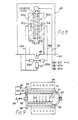
- Fig. 1 is a schematic, cross-sectional view of glow discharge apparatus having a known electrode arrangement for coating cylindrical drums;
- Figs. 2, 3 and 4 are cross-sections of three embodiments of an amorphous silicon photoreceptor made with the apparatus of Fig. 1 in which thicknesses of layers have been exaggerated,
- Fig. 5 is a cross-section of an amorphous silicon photoreceptor deposited on a semi-transparent substrate;
- Fig. 6 is a cross-section of an electrophoto- ghraphic copy machine which uses the amorphous silicon photoreceptor of Fig. 3,
- Fig. 7 is a cross-section illustrating schematically glow discharge apparatus for simulataneously coating or etching a plurality of cylindrical drums, using a known electrode arrangement;
- Fig. 7A shows apparatus according to the invention, for coating or etching a plurality of cylindrical drums,
- Fig. 8 is a side view in cross-section illustrating schematically glow discharge apparatus according to the invention for coating planar members, and
- Fig. 9 is a cross-sectional view of glow discharge apparatus according to the invention for simulataneously coating or etching a plurality of planar substrates.
- Referring to Fig. 1 a glow discharge apparatus is positioned on a
header plate 12 which is hermetically sealed to an enclosure 6. Acylindrical drum 1 of aluminium having anouter surface 11 to be coated is supported in the enclosure 6 by aceramic post 3. Ends discs 2a, b are fitted into the open ends of thecylinder 1. The disc 2b is connected to thecentre conductor 13 of theceramic post 3, which electrically connects thecylinder 1 to the negative terminal of apower supply 10. Theceramic post 3 is hermetically sealed into theheader 12. Counter electrodes 4a, b of, for instance, stainless steel tubing, are supported byceramic posts 19a, b respectively,posts 19a, b being hermetically sealed into theheader 12. The center conductors 8a, b ofposts 19a, b electrically connect the counter electrodes 4a, b respectively to the positive terminal of thepower supply 10 through protective impedances 17a, b respectively. A heating element 9 mounted inside thecylinder 1 is electrically connected through suitable terminals (not shown) to an external power source (not shown). Heating elements 14a, b are mounted inside the counter electrodes 4a, b and are connected through suitable terminals (not shown) inheader 12 to an external power source (not shown). - The enclosure 6 may be evacuated by a vacuum . pump (not shown) by way of a
tube 7, before gases G from gas supply tanks (not shown) are introduced into the enclosure 6 through appropriate valves 16a, b ... z, via aline 15, hermetically fitted in theheader 12, and a second line 5. - In operation, the atmosphere in enclosure 6 is evacuated through
tubing 7 to a pressure of about 1.36 mPa (0.1 Torr) or less and the enclosure 6 is back-filled with the desired film-forming gases G. Various coatings may be produced in the apparatus of Fig. 1 such as, for example, the photoreceptor illustrated in Fig. 2. - Referring now to Fig. 2, a
substrate surface 21 is coated first with an n-type layer 22 of a a-Si:H using gases G consisting of a mixture of silane (SiH4) and phosphine (PH3). The P/Si mixture, which is in the ratio of 0.01% to 1% or greater, is admitted into the line 5 by adjusting the valves 16a, b. The gases G may be diluted, for example, to 5% SiH4 in He and 1% PH3 in He and operated in the pressure range of 13.6 to 41.0 mPa (1 to 3 Torr). The temperature ofsubstrate 1 is maintained at 230°C or higher by adjusting the current to heater 9. Counter electrodes 4a, b may be 200°C or higher by adjusting heaters 14a, b to increase the electrical conductivity of the material deposited on the surfaces of counter electrodes 4a, b during deposition which would otherwise impede the flow of current from the plasma to the anodes 4a, b. Thelayer 22 may be coated to 30 nm and thicker by adjusting voltage V to about 360 volts and maintaining a current density of 0.1 mA/cm2 for about one minute or longer. - Next, the phosphine flow valve 16b is closed and the SiH4 continues to form an intrinsic a-Si:
H layer 23 to attain the desired thickness, dependent on the desired operating voltage of the final device. The SiH4 valve 16a is closed and the enclosure 6 is evacuated. NH3 is then admitted through the valve 16c to a pressure of about 2.73 mPa (0.2 Torr) and the glow discharge continued for about 30 minutes withpower source 10 adjusted to 300 volts and the current I of 0.1 mA/cm2 and higher, thereby forming a nitride ofsilicon layer 24 in a similar manner to that described in the above mentioned U.S. patent no. 4,226,897. - Under test, using a one pm thick a-Si:
H layer 23, a surface voltage Vs of -30 volts was produced in the dark using a conventional Corotron corona charger. No positive charging was noted. Without thenitride layer 24, a surface voltage Vs of only about -15 volts was produced with the same thickness of a-Si:H layer 22. Next, under illumination of 0.2 microjoules at 550 nm, the surface voltage Vs of the photoreceptor with thenitride layer 24, decreased to approximately zero. Finally, thedrum 1 coated as shown in Fig. 2 was used in a commercially available electrophotographic office copier in place of the conventional selenium drum. When thedrum 1 was negatively charged, exposed, and developed with liquid toner by the Carlson method, it produced high quality toned images which transferred to standard paper. - Thus, in the dark, the nitride layer appears to block the flow of holes from the aluminium substrate as well as to block the holes which are generated thermally in the a-Si:H layer from flowing to the surface. Significantly, the charge carriers generated by illumination appear to tunnel through the
nitride layer 24 and discharge the Vs to a low value, indicating that the dielectric layer possesses rectification properties. - Referring now to Fig. 3, a photoreceptor is illustrated having a
surface 31 of thesubstrate 1 which, for example, may be the aluminium drum illustrated in Fig. 1. First, a p+ semiconductor layer 32 is deposited on thesurface 31 in the apparatus of Fig. 1 having a B/Si ratio preferably in the range of 0.01% to 1% with a thickness range of 30 nm to 1 pm. During deposition the temperature is maintained in the range of 250° to 450°C. The higher temperatures are preferred initially for best adhesion to thesubstrate surface 31, after which the temperature is preferably reduced to 250°C. At the higher temperatures, chemical vapour deposition (CVD) was noted to occur by pyrolysis on thesubstrate surface 31 and, indeed, suitable p+ layers 32 were produced at 450°C without applying the glow discharge. A nitride ofsilicon layer 33 was then produced on the p+ layer 32 by a glow discharge in NH3 for 30 minutes, as described above. Finally, the temperature of thesubstrate 1 was held at 250°C and an intrinsic a-Si:H layer 34 of about 5 pm thickness was plasma deposited on thenitride layer 33 by a glow discharge in silane, thereby providing layers in the following sequence: Intrinsic a-Si:H/dielectric/p+ a-Si:H. - Under test, the photoreceptor illustrated in Fig. 3 with a 5 11m thick intrinsic a-Si:
H layer 34 was charged in the dark to a Vs of +80 volts. Surprisingly, the same photoreceptor could be charged in the dark to a Vs of -110 volts. Both polarities of Vs discharged to a few volts under illumination of 2 microjoules at 550 nm. Without thenitride layer 33, Vs onlayer 34 charged in the dark to less than +25 volts, and charged negatively to only a few volts. Thedielectric layer 33 appears to block charge carriers present in the dark, while to be conducting to charge carriers generated by electromagnetic radiation when charged to either polarity. Thus, the dielectric film has properties analogous to a rectifier, except that the effect is independent of polarity. - Indeed, in a further experiment, a top semi- transparent electrode of Cr was evaporated on the intrinsic a-Si:
H layer 34 to form a photodiode structure; and, when an external voltage of 10 volts was applied between the semitransparent electrode and substrate, the current flowing in the dark was less than a microamp, whereas under illumination several milliamps were measured. - Next, the gases G containing a mixture of silane and NH3 were admitted simultaneously during the glow discharge to form a SixNy dielectric film. The discharge was maintained for about 6 minutes to deposit a 100 nm SixNy layer 33 on
p layer 32. Similar dark Vs and illuminated discharge values were obtained to those described above when thedielectric layer 33 was produced by discharging in NH3 alone. - In addition to producing positive and negative charging, the photoreceptor illustrated in Fig. 3 is the preferred embodiment of the invention, since the
dielectric layer 33 is positioned between two semiconductor layers and, therefore,dielectric layer 33 is protected from the mechanical wear involved during the toning, image transfer, and cleaning cycles of the Carlson process. Also under test in a commercial electrophotographic copy machine, high quality images were produced. - Referring to Fig. 4, a p-
type layer 42 is applied to thesurface 41 ofsubstrate 40, after which a SixNy layer 43 is applied to the surface oflayer 42, as described in connection with Fig. 3. An n-type layer 44 in the range of 30 nm to 1 pm thick was applied to the surface of a SixNy layer 43 and an intrinsic a-Si:H layer 45 applied to thelayer 44. Thus the photoreceptor had layers in the following sequence: intrinsic a-Si:H/n a-Si:H/di- electric/p a-Si:H/metal substrate. - Under corotron charging, a negative Vs of -20 volts was accepted by a
layer 44 of one pm thickness. No positive charging was observed since the negative majority carriers in the n-type layer inlayer 44 drift to a positive charge. However, thedielectric layer 43 increased in the Vs by blocking holes from the p-layer and from thesubstrate 11. Again, there is no residual voltage under illumination since the photo-induced charge carriers appear to tunnel throughdielectric layer 42. - Referring to Fig. 5, the
substrate 1 is aglass plate 51 with a semi-transparent, conducting- metal-oxide coating 52 composed of, for example, fluorinated tin oxide 150 nm thick. Thecoating 52 may be coated with aprotective layer 53 of 3 nm silicon oxide formed by oxidizing a plasma deposited a-Si:H layer. - Next, with the
substrate 1 held at 250°C the layers described in connection with Fig. 3 were applied sequentially to theoxide layer 53; i.e., a p-type a-Si:H layer 54, annitride layer 55, an intrinsic a-Si:H layer 56. - In operation the photoreceptor illustrated in Fig. 5 charged to Vs of +50 volts and -70 volts in the dark and discharged to a low value under illumination as low as 0.2 microjoules/cm2 when the thickness of the intrinsic a-Si:
H layer 56 was similar to that described in connection with Fig. 3. - The devices illustrated in Figs. 2-5 were next plasma deposited in the apparatus illustrated in U.S. Patent No. 3,069,283 using a uniform electric field, and similar results were found to those described above. Also, the silane used to produce the intrinsic, n-type, and p-type layers was replaced with the following gases: disilane, fluorosilane, and fluorodisilane. In each case the photoreceptor produced similar results under test to those obtained with silane-He mixture. Also, when the
power source 10 illustrated in Fig. 1 was charged to 60 Hz, audio frequencies from 60 to 20 Hz or radio frequencies from 20 Hz to 200 MHz and photoreceptors were produced such as illustrated in Figs. 2-5, similar results were found. Finally, a-Si:H produced by sputtering or evaporating Si in a hydrogen atmosphere gave similar results. - Referring to Fig. 6, a cross-sectional view of an electrostatic copier particularly suited to the present photoreceptor is illustrated schematically. A
rotating drum 61 mounted on an appropriate shaft moves the a-Si:H photoreceptor 62 produced, for example, as described in connection with Fig. 3. Positioned around the periphery ofdrum 61 are a corotron charging unit 63, anexposure station 64, atoner development system 65 with its development electrode adjusted to the appropriate potential, a paper transfer station 67 with anappropriate transfer corona 67a, and a cleaningstation 66.Paper feed rollers 68 hold the paper 68a against the drum under the transfer corona station 67 as is well known in the art. An erase lamp may be used as illustrated. - In operation with an a-Si:H photoreceptor such as described in connection with Fig. 3, high quality images were obtained with a Vs as low as 80 volts when a typewritten letter was copied onto the surface of the
photoreceptor 62. When an insulating Mylar belt was added to the surface ofphotoreceptor 62 and a corona charger (not shown) was added to the exposure station, good images were obtained for Vs as low as 50 volts. - Next, referring to the
exposure station 64, the optics for imaging a page ontophotoreceptor 64 were removed and a He-Ne laser (not shown) was installed in theexposure station 64 and raster scanned across the a-Si:H surface 61, while being modulated with an acousto-optic modulator in accordance with a data stream, as is known in the art. Again, high resolution spots or images were transferred to the paper with a conventional treated surface for liquid toner. Both analog images and digital spots were recorded successfully. - Finally, referring to Fig. 7, a cross-sectional view of glow discharge apparatus mounted in
enclosure 79 hermetically sealed toheader 78 is illustrated schematically. A pair of drums 70a, b to be coated are connected by leads 76a, b respectively to anelectrical transformer 77.Electrodes 71a, b alternatively function as anode and cathode during each half cycle of the voltage induced on thetransformer 77. The drums 70a, b are supported by shafts 72a, b mounted in bearings (not shown) which are supported on theheader plate 78 byinsulated blocks 73a, b respectively. The drums 70a, b havesurfaces 71a, b to be plasma coated from film-forming gases. Thetransformer 77 is connected to the drums 70a, b throughprotective impedances 75a, b and leads 76a, b which may be conveniently connected to the shafts 72a, b respectively through bearings (not shown) or other sliding contacts. Film-forming gases G are introduced as illustrated into the vicinity of drums 70a, b fromline 74 and appropriate flow controllers FC and feed tanks (not shown). - The method of operation of the deposition system of Fig. 7 is similar to that of the system of Fig. 1 in that the film forming gases are introduced into the region of the drum surfaces 71a, b through
line 74 and flow controllers FC from tanks (not shown), after which the voltage from thetransformer 77 is adjusted to maintain a glow- discharge with the desired current density of, or greater than, 0.1 mAlcm2 and higher. However, both electrodes 70a, b havesubstrate surfaces 71a, b to which the coatings are applied on alternate cycles, thereby eliminating the necessity for a counter electrode which otherwise would wastfully collect some deposit. The frequency of the power from a power source (not shown) applied totransformer 77 may be in the range of 60 Hz to 100 MHz with appropriate matching networks. The drums may be rotated by an external motor (not shown) and drive shafts (not shown) to produce a uniform discharge. Although the cathode glow around thedrum surface 71 a or b connected during its negative half cycle can be adjusted to produce a uniform deposition, the opposingdrum 71a or b is anodic for that half cycle, and its deposit occurs on the area closest to the cathode. However, rotation ofdrums 71a, b then produced uniform coatings. - In tests, all analog and homolog molecules of silane, H2, and the halogens were found to produce useful films as well as dopants and other film-forming gases available commercially.
- In addition, referring to Fig. 7A it was found that when leads 76a, b electrically connected both the drums 70a, b to the negative terminal of
D.C. power supply 180 while the positive terminal was connected toheader 78 ormetallic gas line 74, an improved glow discharge occurred to the drum surfaces 71a, b. Indeed, when the separation S between thesurfaces 71 a, b, as designated by "S" in Fig. 7A was varied and the current was maintained constant, the voltage required to sustain the glow discharge decreased when the separation S was adjusted so that the cathode glows abovesurfaces 71a, b approached one another. Under these conditions less power is required and better film quality insurfaces 71a, b was attained. - In operation, the heaviest deposit was noted to occur in the region of closest separation; however, nonuniformity in thickness was averaged out by rotation of drums 70a, b as shown. Similar results were obtained with a pulsating
D.C. supply 180, and with an A.C. or R.F. supply with a negative bias preferably on drums 70a, b. - Finally, referring to Fig. 8, the drums 70a, b illustrated in Fig. 7A were replaced with flat plate substrates 80a, b, having a separation S between opposing
surfaces 81a, b. As described above, film forming gases from tanks (not shown) are admitted through flow controllers 82a, b, c, through aline 83 in theheader 84 into the vicinity of thesubstrate surfaces 81a, b. Theencosure 85 is evacuated through theline 86 by a vacuum pump (not shown) as described above. One terminal of a power supply 87 is connected through leads 88a, b to the substrates 80a, b respectively, through protective impedances 89a, b. The other terminal of the power supply 87 is connected to the header or to thegas supply lead 83 which acts as the counter electrode. Heaters 91a, b in the substrates 80a, b are powered by an external power source (not shown) to maintain the desired substrate temperature, or an external source may radiantly heat substrates 80a, b. - In operation, the desired film forming gases such as, for example, silane and its dopants, as described in connection with Fig. 3, are admitted through
line 83 into theenclosure 85. The power supply 87 may be pulsating D.C. with the most negative polarity connected through the leads 88a, b to the substrates 80a, b to maintain a glow discharge aroundsubstrate surfaces 81a, b. When the separation S is adjusted to position the negative glow regions abovesurfaces 81 a, b in close proximity to one another, the voltage from power source 87 required to maintain the same current was observed to decrease. For example, using 101.6 mm x 203.2 mm (4" x 8") aluminium plate substrates 80a, b and 5% silane in He at 27.3 mPa (2 Torr) pressure, the voltage required to sustain 50 mA decreased from 360 to 340 volts when the separation S was decreased from 50.8 to 25.4 mm (2 inches to 1 inch). - Under test, uniform films with good semiconductor properties were noted. Other gases gave similar results provided the cathode glows on the substrate surfaces were adjusted in close or overlapping proximity. (The effect was useful until the separation S was so small the glow discharge was extinguished). Under such conditions the apparatus illustrated in Fig. 8 was found to deposit improved a-Si:H films from silane, disilane, Sif4, difluorosilane and various combinations of dopants including hydrogen, fluorine, diborane, phosphine and arsine. Other semiconductor gases found to deposit improved films included germane and trimethyl gallium with arsine.
- In addition, when a silicon wafer was placed on the surface 81 of the
electrode 80 in the apparatus illustrated in Fig. 8 and the reactive gases that are etchants of Si such as, for example, CH4 and 02, were introduced throughtube 83, rapid etching of Si, Si02 and Si3N4 was observed under glow discharge. Also, BC13 was found to etch AI layers on Si. Introduction 02 alone was found to form Si02 on a Si wafer during a glow discharge and the addition of a few percent of CF4 enhanced the oxidation rate. Although this etching reaction is similar to that known in the art, the apparatus of Fig. 8 was found to reduce the power required to operate in a stable manner at lower pressures and to produce better anisotropic etching than conventional parallel planar reactors or inductively coupled reactors. - Referring to Fig. 9, a number of
substrates 91, such as Si wafers, are held in a conductingtray 92 which is electrically connected to theheader 94 and to ground. Theheader 94 forms a vacuum- tight enclosure with aquartz tube 93 by means of a gasket (not shown). The conductingwafer tray 92 may be cantilevered from theheader 94. AnIR oven 98 positioned aroundquartz tube 93 may be used toradiantly heat substrate 91. Gases G are admitted from tanks (not shown) and aflow controller 99 throughtubing 96 in theheader 94 and past thesubstrates 91. The reaction byproducts of gases G are exhausted throughtubing 95 by a vacuum pump (not shown). - To provide an electric field to the
substrates 91, acounter electrode 97 in the form of nickel tubing is mounted on an electrical feed-through 101 in theheader 94. The center conductor of the feed-through 101 may be connected to the positive terminal of apower supply 102, the negative terminal of which may be grounded toheader 94. - Again, as described in connection with Fig. 7 and Fig. 8, the separation S between
substrates 91 is adjusted for the desired pressure of gases G so that the cathode glow regions have juxtaposed surfaces ofsubstrates 91 are in sufficiently close proximity to interact and reduce the voltage required for deposition or etching. Thesubstrates 91 may be of any desired material instead of the Si wafers and gases G may be any mentioned above or others, deposition or etching being determined by the gases G being used. Also, pulsating D.C., A.C., or R.F. power supplies may be used between thesubstrates 91 and thecounter electrode 97, although the enhanced glow discharge only occurs during the portion of the voltage cycles in which substrates 91 are negative relative to counterelectrode 97. - In addition to using the well known Carlson method of toning the electrostatic images on the photoreceptors, it was found that by coating the photoreceptors illustrated in Figs. 2-5 with a conventional thermoplastic polymer and then corona charging them, a physcial image was produced in the polymer. Specifically, when the photoreceptor was exposed to a light image from, say, a laser beam, the surface charge was selectively discharged. The application of heat to the softening point of the polymer then permitted the portion of the surface which retained charge to physically deform in accordance with the charge pattern. The pattern was then read by a laser, as is known in the art.
Claims (14)
Applications Claiming Priority (2)
| Application Number | Priority Date | Filing Date | Title |
|---|---|---|---|
| US284333 | 1981-07-17 | ||
| US06284333 US4484809B1 (en) | 1977-12-05 | 1981-07-17 | Glow discharge method and apparatus and photoreceptor devices made therewith |
Publications (2)
| Publication Number | Publication Date |
|---|---|
| EP0070715A1 EP0070715A1 (en) | 1983-01-26 |
| EP0070715B1 true EP0070715B1 (en) | 1987-03-18 |
Family
ID=23089803
Family Applications (1)
| Application Number | Title | Priority Date | Filing Date |
|---|---|---|---|
| EP82303757A Expired EP0070715B1 (en) | 1981-07-17 | 1982-07-16 | Glow discharge method and apparatus and photoreceptor devices made therewith |
Country Status (4)
| Country | Link |
|---|---|
| US (1) | US4484809B1 (en) |
| EP (1) | EP0070715B1 (en) |
| JP (1) | JPH067269B2 (en) |
| DE (1) | DE3275764D1 (en) |
Cited By (3)
| Publication number | Priority date | Publication date | Assignee | Title |
|---|---|---|---|---|
| SG97169A1 (en) * | 1999-12-07 | 2003-07-18 | Applied Materials Inc | Method and apparatus for reducing fixed charges in a semiconductor device |
| US6794311B2 (en) | 2000-07-14 | 2004-09-21 | Applied Materials Inc. | Method and apparatus for treating low k dielectric layers to reduce diffusion |
| US7144606B2 (en) | 1999-06-18 | 2006-12-05 | Applied Materials, Inc. | Plasma treatment to enhance adhesion and to minimize oxidation of carbon-containing layers |
Families Citing this family (14)
| Publication number | Priority date | Publication date | Assignee | Title |
|---|---|---|---|---|
| US4666808A (en) * | 1983-04-01 | 1987-05-19 | Kyocera Corp. | Amorphous silicon electrophotographic sensitive member |
| JPS6011849A (en) * | 1983-06-21 | 1985-01-22 | Sanyo Electric Co Ltd | Electrostatic latent image bearing material |
| DE3481225D1 (en) * | 1983-09-30 | 1990-03-08 | Mita Industrial Co Ltd | ELECTROPHOTOGRAPHIC DEVICE, CONTAINING A LIGHT SENSITIVE LAYER OF AMORPHOUS SILICON LIGHT GUIDE. |
| US4657374A (en) * | 1984-06-23 | 1987-04-14 | Matsushita Electric Industrial Co., Ltd. | Development system for photoreceptor having surface potential and a large amount of charge |
| US4619877A (en) * | 1984-08-20 | 1986-10-28 | Eastman Kodak Company | Low field electrophotographic process |
| US4607937A (en) * | 1984-11-16 | 1986-08-26 | Sanyo Electric Co., Ltd. | Electrostatic recording apparatus |
| DE3681862D1 (en) * | 1985-08-23 | 1991-11-14 | Siemens Ag | METHOD FOR PRODUCING A HIGHLY LOCKING DIODE ARRANGEMENT BASED ON A-SI: H FOR IMAGE SENSOR LINES. |
| JPS62258464A (en) * | 1986-04-08 | 1987-11-10 | Canon Inc | light receiving member |
| US4737429A (en) * | 1986-06-26 | 1988-04-12 | Xerox Corporation | Layered amorphous silicon imaging members |
| US5178063A (en) * | 1986-12-16 | 1993-01-12 | L & C Family Partnership | Method and apparatus for automatic numbering of forms on a rotary printing press |
| US5001500A (en) * | 1986-12-16 | 1991-03-19 | L & C Family Partnership | Endless belt printing apparatus |
| US6282400B1 (en) * | 1998-06-01 | 2001-08-28 | Canon Kabushiki Kaisha | Image-forming apparatus and image forming method using a controlled dynamic frictional force between a cleaning blade and a photosensitive member |
| JP4133408B2 (en) * | 2003-02-14 | 2008-08-13 | 株式会社東芝 | Induction heating cooker |
| GB201110906D0 (en) | 2011-06-27 | 2011-08-10 | Amazon Bio Guard Ltd | A portable apparatus for generating and broadcasting an aerosol mist |
Family Cites Families (24)
| Publication number | Priority date | Publication date | Assignee | Title |
|---|---|---|---|---|
| US3017251A (en) * | 1958-08-19 | 1962-01-16 | Du Pont | Process for the production of silicon |
| GB903021A (en) * | 1959-07-17 | 1962-08-09 | Standard Telephones Cables Ltd | Improvements in or relating to the production of silicon |
| DE2746967C2 (en) * | 1977-10-19 | 1981-09-24 | Siemens AG, 1000 Berlin und 8000 München | Electrophotographic recording drum |
| DE2753750C2 (en) * | 1977-12-02 | 1982-12-23 | Hoechst Ag, 6000 Frankfurt | Device for the surface treatment of foil webs by means of electrical corona discharge |
| US4226897A (en) * | 1977-12-05 | 1980-10-07 | Plasma Physics Corporation | Method of forming semiconducting materials and barriers |
| US4265991A (en) * | 1977-12-22 | 1981-05-05 | Canon Kabushiki Kaisha | Electrophotographic photosensitive member and process for production thereof |
| DE2803331C3 (en) * | 1978-01-26 | 1981-09-03 | Klöckner Ionon GmbH, 5000 Köln | System for the partial treatment of elongated workpieces by means of a high-current glow discharge |
| JPS54126676A (en) * | 1978-02-21 | 1979-10-02 | Ici Ltd | Chemical method on surface of rotating article |
| GB2018446B (en) * | 1978-03-03 | 1983-02-23 | Canon Kk | Image-forming member for electrophotography |
| JPS54145537A (en) * | 1978-05-04 | 1979-11-13 | Canon Inc | Preparation of electrophotographic image forming material |
| JPS54145539A (en) * | 1978-05-04 | 1979-11-13 | Canon Inc | Electrophotographic image forming material |
| JPS5511330A (en) * | 1978-07-08 | 1980-01-26 | Shunpei Yamazaki | Semiconductor device having continuous junction |
| US4202928A (en) * | 1978-07-24 | 1980-05-13 | Rca Corporation | Updateable optical storage medium |
| US4200666A (en) * | 1978-08-02 | 1980-04-29 | Texas Instruments Incorporated | Single component monomer for silicon nitride deposition |
| US4363828A (en) * | 1979-12-12 | 1982-12-14 | International Business Machines Corp. | Method for depositing silicon films and related materials by a glow discharge in a disiland or higher order silane gas |
| JPS56146142A (en) * | 1980-04-16 | 1981-11-13 | Hitachi Ltd | Electrophotographic sensitive film |
| JPS56150752A (en) * | 1980-04-25 | 1981-11-21 | Hitachi Ltd | Electrophotographic sensitive film |
| JPS574053A (en) * | 1980-06-09 | 1982-01-09 | Canon Inc | Photoconductive member |
| JPS574172A (en) * | 1980-06-09 | 1982-01-09 | Canon Inc | Light conductive member |
| JPS5727263A (en) * | 1980-07-28 | 1982-02-13 | Hitachi Ltd | Electrophotographic photosensitive film |
| US4394426A (en) * | 1980-09-25 | 1983-07-19 | Canon Kabushiki Kaisha | Photoconductive member with α-Si(N) barrier layer |
| US4341582A (en) * | 1980-12-22 | 1982-07-27 | The Perkin-Elmer Corporation | Load-lock vacuum chamber |
| JPS57115552A (en) * | 1981-01-08 | 1982-07-19 | Nippon Telegr & Teleph Corp <Ntt> | Electrophotographic receptor |
| US4409311A (en) * | 1981-03-25 | 1983-10-11 | Minolta Camera Kabushiki Kaisha | Photosensitive member |
-
1981
- 1981-07-17 US US06284333 patent/US4484809B1/en not_active Expired - Lifetime
-
1982
- 1982-07-16 DE DE8282303757T patent/DE3275764D1/en not_active Expired
- 1982-07-16 JP JP57124266A patent/JPH067269B2/en not_active Expired - Lifetime
- 1982-07-16 EP EP82303757A patent/EP0070715B1/en not_active Expired
Cited By (3)
| Publication number | Priority date | Publication date | Assignee | Title |
|---|---|---|---|---|
| US7144606B2 (en) | 1999-06-18 | 2006-12-05 | Applied Materials, Inc. | Plasma treatment to enhance adhesion and to minimize oxidation of carbon-containing layers |
| SG97169A1 (en) * | 1999-12-07 | 2003-07-18 | Applied Materials Inc | Method and apparatus for reducing fixed charges in a semiconductor device |
| US6794311B2 (en) | 2000-07-14 | 2004-09-21 | Applied Materials Inc. | Method and apparatus for treating low k dielectric layers to reduce diffusion |
Also Published As
| Publication number | Publication date |
|---|---|
| EP0070715A1 (en) | 1983-01-26 |
| US4484809A (en) | 1984-11-27 |
| JPH067269B2 (en) | 1994-01-26 |
| US4484809B1 (en) | 1995-04-18 |
| DE3275764D1 (en) | 1987-04-23 |
| JPS5837648A (en) | 1983-03-04 |
Similar Documents
| Publication | Publication Date | Title |
|---|---|---|
| US4484809A (en) | Glow discharge method and apparatus and photoreceptor devices made therewith | |
| US4634648A (en) | Electrophotographic imaging members with amorphous carbon | |
| US5534070A (en) | Plasma CVD process using a very-high-frequency and plasma CVD apparatus | |
| EP0717127B1 (en) | Plasma processing method and apparatus | |
| US5817181A (en) | Process for forming deposited film for light-receiving member, light-received member produced by the process deposited film forming apparatus, and method for cleaning deposited film forming apparatus | |
| US4569719A (en) | Glow discharge method and apparatus and photoreceptor devices made therewith | |
| US5129359A (en) | Microwave plasma CVD apparatus for the formation of functional deposited film with discharge space provided with gas feed device capable of applying bias voltage between the gas feed device and substrate | |
| US6435130B1 (en) | Plasma CVD apparatus and plasma processing method | |
| US5958644A (en) | Process to form light-receiving member with outer layer made by alternately forming and etching | |
| US4613556A (en) | Heterogeneous electrophotographic imaging members of amorphous silicon and silicon oxide | |
| WO2006134781A1 (en) | Method and device for depositing film, deposited film and photosensitive body employing same | |
| US4741801A (en) | Glow discharge method and apparatus and photoreceptor devices made therewith | |
| JP4562163B2 (en) | Method for producing electrophotographic photosensitive member and electrophotographic photosensitive member | |
| US5108860A (en) | Electrophotographic recording material and method for the manufacture thereof | |
| US4698288A (en) | Electrophotographic imaging members having a ground plane of hydrogenated amorphous silicon | |
| US4758487A (en) | Electrostatographic imaging members with amorphous boron | |
| JP2994658B2 (en) | Apparatus and method for forming deposited film by microwave CVD | |
| JP2867150B2 (en) | Microwave plasma CVD equipment | |
| JPH1060653A (en) | Method for forming deposited film by high frequency plasma CVD method | |
| JPH04247877A (en) | Deposited film forming device | |
| JP3122008B2 (en) | Method and apparatus for forming deposited film | |
| JP2784784B2 (en) | Method and apparatus for forming functional deposited film by microwave plasma CVD | |
| KR0156562B1 (en) | Manufacturing method of electrophotographic photosensitive member | |
| JP2925310B2 (en) | Deposition film formation method | |
| JP3257575B2 (en) | Deposited film forming apparatus and deposited film forming method |
Legal Events
| Date | Code | Title | Description |
|---|---|---|---|
| PUAI | Public reference made under article 153(3) epc to a published international application that has entered the european phase |
Free format text: ORIGINAL CODE: 0009012 |
|
| AK | Designated contracting states |
Designated state(s): DE FR GB NL |
|
| 17P | Request for examination filed |
Effective date: 19830608 |
|
| GRAA | (expected) grant |
Free format text: ORIGINAL CODE: 0009210 |
|
| AK | Designated contracting states |
Kind code of ref document: B1 Designated state(s): DE FR GB NL |
|
| REF | Corresponds to: |
Ref document number: 3275764 Country of ref document: DE Date of ref document: 19870423 |
|
| ET | Fr: translation filed | ||
| PLBE | No opposition filed within time limit |
Free format text: ORIGINAL CODE: 0009261 |
|
| STAA | Information on the status of an ep patent application or granted ep patent |
Free format text: STATUS: NO OPPOSITION FILED WITHIN TIME LIMIT |
|
| 26N | No opposition filed | ||
| PGFP | Annual fee paid to national office [announced via postgrant information from national office to epo] |
Ref country code: DE Payment date: 20010709 Year of fee payment: 20 |
|
| PGFP | Annual fee paid to national office [announced via postgrant information from national office to epo] |
Ref country code: GB Payment date: 20010711 Year of fee payment: 20 |
|
| PGFP | Annual fee paid to national office [announced via postgrant information from national office to epo] |
Ref country code: FR Payment date: 20010712 Year of fee payment: 20 |
|
| PGFP | Annual fee paid to national office [announced via postgrant information from national office to epo] |
Ref country code: NL Payment date: 20010730 Year of fee payment: 20 |
|
| REG | Reference to a national code |
Ref country code: GB Ref legal event code: IF02 |
|
| PG25 | Lapsed in a contracting state [announced via postgrant information from national office to epo] |
Ref country code: GB Free format text: LAPSE BECAUSE OF EXPIRATION OF PROTECTION Effective date: 20020715 |
|
| PG25 | Lapsed in a contracting state [announced via postgrant information from national office to epo] |
Ref country code: NL Free format text: LAPSE BECAUSE OF EXPIRATION OF PROTECTION Effective date: 20020716 |
|
| REG | Reference to a national code |
Ref country code: GB Ref legal event code: PE20 Effective date: 20020715 |
|
| NLV7 | Nl: ceased due to reaching the maximum lifetime of a patent |
Effective date: 20020716 |