EP0068883A2 - A level converter circuit - Google Patents
A level converter circuit Download PDFInfo
- Publication number
- EP0068883A2 EP0068883A2 EP82303392A EP82303392A EP0068883A2 EP 0068883 A2 EP0068883 A2 EP 0068883A2 EP 82303392 A EP82303392 A EP 82303392A EP 82303392 A EP82303392 A EP 82303392A EP 0068883 A2 EP0068883 A2 EP 0068883A2
- Authority
- EP
- European Patent Office
- Prior art keywords
- bipolar transistor
- level
- converter circuit
- level converter
- transistor
- Prior art date
- Legal status (The legal status is an assumption and is not a legal conclusion. Google has not performed a legal analysis and makes no representation as to the accuracy of the status listed.)
- Granted
Links
Images


Classifications
-
- H—ELECTRICITY
- H03—ELECTRONIC CIRCUITRY
- H03K—PULSE TECHNIQUE
- H03K19/00—Logic circuits, i.e. having at least two inputs acting on one output; Inverting circuits
- H03K19/02—Logic circuits, i.e. having at least two inputs acting on one output; Inverting circuits using specified components
- H03K19/08—Logic circuits, i.e. having at least two inputs acting on one output; Inverting circuits using specified components using semiconductor devices
- H03K19/094—Logic circuits, i.e. having at least two inputs acting on one output; Inverting circuits using specified components using semiconductor devices using field-effect transistors
- H03K19/0944—Logic circuits, i.e. having at least two inputs acting on one output; Inverting circuits using specified components using semiconductor devices using field-effect transistors using MOSFET or insulated gate field-effect transistors, i.e. IGFET
- H03K19/09448—Logic circuits, i.e. having at least two inputs acting on one output; Inverting circuits using specified components using semiconductor devices using field-effect transistors using MOSFET or insulated gate field-effect transistors, i.e. IGFET in combination with bipolar transistors [BIMOS]
-
- H—ELECTRICITY
- H03—ELECTRONIC CIRCUITRY
- H03K—PULSE TECHNIQUE
- H03K19/00—Logic circuits, i.e. having at least two inputs acting on one output; Inverting circuits
- H03K19/0175—Coupling arrangements; Interface arrangements
- H03K19/017509—Interface arrangements
- H03K19/017518—Interface arrangements using a combination of bipolar and field effect transistors [BIFET]
Definitions
- the present invention relates to a level converter circuit, more particularly to a level converter circuit which converts the signal level being output from an integrated circuit (IC) memory device and the like into another arbitrary signal level.
- IC integrated circuit
- TTL transistor-transistor logic
- MOS metal oxide semiconductor
- ECL emitter coupled logic
- ECL emitter coupled logic
- the output signals of a random access memory (RAM) consisting of MOS IC's may be coupled with the inputs of a logic circuit consisting of ECL IC's. In such a case, it is necessary to convert the TTL signal level into an ECL signal level.
- RAM random access memory
- ground potential V SS is used as the base potential, for example, 0 V
- voltage V CC higher than ground potential V SS by, for example, 5 V is used as the voltage supply.
- ground potential V SS is used as the base potential, for example, 0 V
- voltage V EE lower than ground potential V SS for example, -5.2 V is used as the voltage supply.
- a prior art level converter circuit used for converting TTL level into the ECL level is illustrated in Fig. 1.
- the level converter circuit of Fig. 1 comprises buffer circuit B 1 , PNP transistor Q 1 , and resistors R 1 , R 2 , and R 3 .
- the operation of the level converter circuit of Fig. 1 is illustrated in Fig. 2.
- the input signal supplied to the input terminal I.P. of the level converter circuit of Fig. 1 is a TTL level signal in the range between 0 V (V SS ) and + 5.0 V (V CC ), as shown in Fig. 2.
- the maximum level of the low (L) level signal is +0.4 V and the minimum level of the high (H) level signal is +2.4 V.
- the output signal of the level converter circuit of Fig. 1 is an ECL level signal in the range between 0 V (VSS) and -5.2 V (VEE).
- ECL level signal the maximum level of the L level signal is -1.6 V, and the minimum level of the H level signal is -0.8 V.
- H level signal V H1 of the TTL level supplied to input terminal I.P. is converted into H level signal VH2 of the ECL level by the level converter circuit.
- the converted signal is output from output terminal O.P.
- L level signal V L1 of the TTL level supplied to input terminal I.P. is converted into L level signal V L2 of the ECL level by the level converter circuit. That converted signal is output from output terminal O.P..
- An embodiment of the present invention 'can provide a level converter circuit in which the output signal level of the TTL or MOS IC being operated between the two voltage supplies is converted into another signal level, the output signal being able to be supplied to the input of another type of IC, for example, an ECL IC.
- a level converter circuit for converting a first logic signal using a lower voltage supply as abase (or gate) potential into a second logic signal using a higher voltage supply as a base potential; said level converter circuit comprising an input terminal for receiving the first logic signal, an output terminal for outputting the second logic signal, a first bipolar transistor having a collector connected to the higher voltage supply, a second bipolar transistor connected between the higher voltage supply and the output terminal, the second bipolar transistor having a base connected to an emitter of the first bipolar transistor, and means for turning on the second bipolar transistor or both bipolar transistors in response to the first logic signal applied to the input terminal.
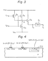
- a level converter circuit in accordance with one embodiment of the present invention is illustrated in Fig. 3.
- the level converter circuit of Fig.3 comprises depression (deplettion) type MOS transistor Q 2 , enhancement type MOS transistor Q 3 , and NPN-type bipolar transistors Q 4 and Q 5 .
- MOS transistors Q 2 and Q 3 are connected in series between voltage supply lines V SS and V EE .
- the gates of MOS transistors Q 2 and Q 3 are connected to input terminals T 1 and T 2 , respectively.
- Conjunction A between the source of MOS transistor Q 2 and the drain of MOS transistor Q 3 is also connected to the emitter of bipolar transistor Q 4 and the base of bipolar transistor Q 5 .
- the collectors of bipolar transistors Q 4 and Q 5 are both connected to voltage supply line V SS .
- the base of bipolar transistor Q 4 is connected to input terminal T 2 .
- the emitter of bipolar transistor Q 5 is connected to output terminal T 3 .
- Output terminal T 3 may be connected to an ECL circuit or another type circuit. In Fig. 3, it is connected to one end of dummy load resistor R L equivalent to an ECL circuit. The other end of resistor R L is connected to external voltage supply terminal T 4 .
- An arbitrary voltage may be applied to terminal T 4 corresponding to dummy load resistor R L .
- resistor R may be 50 ⁇ and the voltage applied to the terminal T 4 may be -2.0 V with regard to voltage supply V SS .
- the level converter circuit may be formed on the same IC semiconductor substrate on which a RAM device is formed.
- Figure 4 illustrates a sectional view of the P-type semiconductor substrate on which MOS transistors Q 2 , Q 3 and bipolar transistor Q 4 are formed. As shown in Fig. 4, NPN transistor Q 4 is formed in the N-well formed in the P-type substrate.
- higher voltage supply line V SS may be the ground potential, for example, 0 V.
- the lower voltage supply line V EE may be -5.2 V.
- Logic signal S 1 alternating between V SS and V EE is applied to input terminal T 1 .
- Inverted signal S 2 of logic signal S 1 is applied to input terminal T 2 .
- the emitter voltage of bipolar transistor Q 5 becomes the value V SS -V BE , that is, the voltage lower than the base voltage of bipolar transistor Q 5 by base-emitter voltage V BB .
- the "H" level voltage of the ECL level is obtained at output terminal T 3 .
- bipolar transistor Q 5 Since the emitter voltage of bipolar transistor Q 4 is applied to the base of bipolar transistor Q 5 , bipolar transistor Q 5 is turned ON, and the emitter voltage of bipolar transistor Q 5 becomes lower than the base voltage by base-emitter voltage V BE of bipolar transistor Q 5 . Thus, the voltage V SS -2V EB is obtained at the output terminal T 3 . This voltage is used as the "L" level signal of the ECL level.
- the output signal of the level converter circuit of Fig. 3 can be directly applied to the input of the typical ECL circuit shown in Fig. 5.
- the ECL circuit of Fig. 5 comprises NPN type bipolar transistors Q 6 , Q 7 , and Q 8 and resistors R 4 and R 5 .
- the level conversion according to the level converter circuit of Fig. 3 is illustrated in Fig. 6.
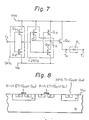
- a level converter circuit in accordance with another embodiment of the present invention is illustrated in Fig. 7.
- the level converter circuit of Fig. 7 comprises P-channel MOS transistors Q 9 and Q 11 , N-channel MOS transistors Q 10 and Q 12 , and NPN type bipolar transistors Q 13 and Q 14 .
- the P-channel MOS transistor Q 9 and the N-channel MOS transistor Q 10 are connected in series between higher voltage supply line V SS and lower voltage supply line V and form a complementary metal-oxide semiconductor (CMOS) inverter INV 1
- CMOS complementary metal-oxide semiconductor
- P-channel MOS transistor Q11 and N-channel MOS transistor Q 12 are also connected in series between voltage supply lines V SS and V EE and form a CMOS inverter INV 2 .
- inverter INV 1 The input of inverter INV 1 is connected to input terminal T , and the output of inverter INV 1 is connected to the input of inverter INV 2 and to the base of bipolar transistor Q 13 .
- the collectors of bipolar transistors Q 13 and Q 14 are both connected to voltage supply line V SS .
- the emitter of bipolar transistor Q 13 and the base of bipolar transistor Q 14 are connected to the output of inverter INV 2 , that is, the conjunction A between the source of MOS transistor Q 11 and the drain of MOS transistor Q 12 .
- the emitter of bipolar transistor Q 14 is connected to output terminal T 6 .
- Output terminal T 6 is connected to external voltage supply terminal T 7 through dummy load resistor R L .
- the level converter circuit of Fig. 7 may be formed on the N-type semiconductor substrate as illustrated in Fig. 8.
- N-channel MOS transistor Q 10 or Q 12 P -channel MOS transistor Q 9 or Q 11 , and NPN type bipolar transistor Q 13 or Q 14 are formed.
- a logic signal is applied to input terminal T 5 .
- V SS the "H" level signal
- V EE the output signal of inverter INV 5 becomes "L” level (V EE ).
- P-channel MOS transistor Q 11 is turned ON, and N-channel MOS transistor Q 12 and bipolar transistor Q 13 are turned OFF
- the base voltage of bipolar transistor Q 14 becomes the V SS level
- the emitter voltage of bipolar transistor Q 14 that is, the voltage of output terminal T 6 , becomes the value V SS -V BE , just as in the circuit of Fig. 3.
- a level converter circuit which consists of MOS transistors and bipolar transistors formed on the same IC substrate; said level converter circuit converting the MOS level signals obtained from the MOS transistors of the inner circuit into an arbitrary voltage level by means of the bipolar transistors.
- the level converter circuit according to the present invention has the following advantages:
Abstract
Description
- The present invention relates to a level converter circuit, more particularly to a level converter circuit which converts the signal level being output from an integrated circuit (IC) memory device and the like into another arbitrary signal level.
- Recently, it is often necessary to couple the output signals of transistor-transistor logic (TTL) or metal oxide semiconductor (MOS) IC's with the inputs of emitter coupled logic (ECL) ICs or to couple the output signals of ECL ICs with the input of TTL or MOS ICs. For example, the output signals of a random access memory (RAM) consisting of MOS IC's may be coupled with the inputs of a logic circuit consisting of ECL IC's. In such a case, it is necessary to convert the TTL signal level into an ECL signal level. Generally, for the TTL level, ground potential VSS is used as the base potential, for example, 0 V, and voltage VCC higher than ground potential VSS by, for example, 5 V is used as the voltage supply. For the ECL level, ground potential VSS is used as the base potential, for example, 0 V, and voltage VEE lower than ground potential VSS , for example, -5.2 V is used as the voltage supply.
- A prior art level converter circuit used for converting TTL level into the ECL level is illustrated in Fig. 1. The level converter circuit of Fig. 1 comprises buffer circuit B1 , PNP transistor Q1 , and resistors R1 , R2 , and R3. The operation of the level converter circuit of Fig. 1 is illustrated in Fig. 2. The input signal supplied to the input terminal I.P. of the level converter circuit of Fig. 1 is a TTL level signal in the range between 0 V (VSS) and +5.0 V (VCC), as shown in Fig. 2. In the TTL level signal, the maximum level of the low (L) level signal is +0.4 V and the minimum level of the high (H) level signal is +2.4 V. The output signal of the level converter circuit of Fig. 1 is an ECL level signal in the range between 0 V (VSS) and -5.2 V (VEE). In the ECL level signal, the maximum level of the L level signal is -1.6 V, and the minimum level of the H level signal is -0.8 V.
- H level signal VH1 of the TTL level supplied to input terminal I.P. is converted into H level signal VH2 of the ECL level by the level converter circuit. The converted signal is output from output terminal O.P. Similarly, L level signal VL1 of the TTL level supplied to input terminal I.P. is converted into L level signal VL2 of the ECL level by the level converter circuit. That converted signal is output from output terminal O.P..
- As described above, in the level converter circuit of Fig. 1, three voltage supply lines +5.0 V, 0 V, and -5.2 V are necessary. However, using three voltage supply lines. is disadvantageous for increasing the integration scale of the IC.
- An embodiment of the present invention 'can provide a level converter circuit in which the output signal level of the TTL or MOS IC being operated between the two voltage supplies is converted into another signal level, the output signal being able to be supplied to the input of another type of IC, for example, an ECL IC.
- In accordance with the present invention, there is provided a level converter circuit for converting a first logic signal using a lower voltage supply as abase (or gate) potential into a second logic signal using a higher voltage supply as a base potential; said level converter circuit comprising an input terminal for receiving the first logic signal, an output terminal for outputting the second logic signal, a first bipolar transistor having a collector connected to the higher voltage supply, a second bipolar transistor connected between the higher voltage supply and the output terminal, the second bipolar transistor having a base connected to an emitter of the first bipolar transistor, and means for turning on the second bipolar transistor or both bipolar transistors in response to the first logic signal applied to the input terminal.
-
- Figure 1 illustrates a circuit diagram of a level converter circuit of a prior art:
- Fig. 2 illustrates the level conversion in the circuit of Fig. 1;
- Fig. 3 illustrates a circuit diagram of a level converter circuit in accordance with one embodiment of the present invention;
- Fig. 4 illustrates a sectional view of a semiconductor substrate on which the circuit of Fig. 3 is formed;
- Fig. 5 illustrates a circuit diagram of a typical ECL circuit;
- Fig. 6 illustrates the level conversion according to an embodiment of the present invention;
- Fig. 7 illustrates a circuit diagram of a level converter circuit in accordance with another embodiment of the present invention; and
- Fig. 8 illustrates the sectional view of a semiconductor substrate on which the circuit of Fig. 7 is formed.
- A level converter circuit in accordance with one embodiment of the present invention is illustrated in Fig. 3. The level converter circuit of Fig.3 comprises depression (deplettion) type MOS transistor Q2 , enhancement type MOS transistor Q3 , and NPN-type bipolar transistors Q4 and Q5.
- In the level converter circuit of Fig. 3, MOS transistors Q2 and Q3 are connected in series between voltage supply lines VSS and VEE. The gates of MOS transistors Q2 and Q3 are connected to input terminals T1 and T2 , respectively. Conjunction A between the source of MOS transistor Q2 and the drain of MOS transistor Q3 is also connected to the emitter of bipolar transistor Q4 and the base of bipolar transistor Q5. The collectors of bipolar transistors Q4 and Q5 are both connected to voltage supply line VSS. The base of bipolar transistor Q4 is connected to input terminal T2. The emitter of bipolar transistor Q5 is connected to output terminal T3.
- Output terminal T3 may be connected to an ECL circuit or another type circuit. In Fig. 3, it is connected to one end of dummy load resistor RL equivalent to an ECL circuit. The other end of resistor RL is connected to external voltage supply terminal T4. An arbitrary voltage may be applied to terminal T4 corresponding to dummy load resistor RL. For example, resistor R may be 50 Ω and the voltage applied to the terminal T4 may be -2.0 V with regard to voltage supply VSS.
- The level converter circuit may be formed on the same IC semiconductor substrate on which a RAM device is formed. Figure 4 illustrates a sectional view of the P-type semiconductor substrate on which MOS transistors Q2 , Q3 and bipolar transistor Q4 are formed. As shown in Fig. 4, NPN transistor Q4 is formed in the N-well formed in the P-type substrate.
- In the level converter circuit of Fig. 3, higher voltage supply line VSS may be the ground potential, for example, 0 V. The lower voltage supply line VEE may be -5.2 V. Logic signal S1 alternating between VSS and VEE is applied to input terminal T1. Inverted signal S2 of logic signal S1 is applied to input terminal T2.
- Thus, when the "H" level signal (V ) is applied to terminal T1 , the "L" level signal (VEE) is applied to terminal T2. In this case, MOS transistor Q2 is turned on, and MOS transistor Q3 and bipolar transistor Q4 are turned OFF. Accordingly, the voltage of conjunction A, that is, the base voltage of bipolar transistor Q5 , becomes the "H" level (V SS) through MOS transistor Q2, and bipolar transistor Q5 is turned ON. Since the emitter of bipolar transistor Q5 is connected to the external voltage supply through dummy load resistor RL , the current flows between the collector and emitter of bipolar transistor Q5. The emitter voltage of bipolar transistor Q5 becomes the value VSS-VBE , that is, the voltage lower than the base voltage of bipolar transistor Q5 by base-emitter voltage VBB. Thus, the "H" level voltage of the ECL level is obtained at output terminal T3.
- Then, when the "L" level signal (VEE) is applied to input terminal T1 and the "H" level signal (VSS) is applied to input terminal T2 , MOS transistor Q2 is turned OFF and MOS transistor Q3 and bipolar transistor Q4 are turned ON. Accordingly, the current flows through bipolar transistor Q4 and MOS transistor Q3 , and the emitter voltage of bipolar transistor Q4 becomes lower than voltage VSS of input terminal T2 by base-emitter voltage VBE of bipolar transistor Q4. Since the emitter voltage of bipolar transistor Q4 is applied to the base of bipolar transistor Q5 , bipolar transistor Q5 is turned ON, and the emitter voltage of bipolar transistor Q5 becomes lower than the base voltage by base-emitter voltage VBE of bipolar transistor Q5. Thus, the voltage VSS-2VEB is obtained at the output terminal T3. This voltage is used as the "L" level signal of the ECL level.
- As described above, the output signal of the level converter circuit of Fig. 3 can be directly applied to the input of the typical ECL circuit shown in Fig. 5. The ECL circuit of Fig. 5 comprises NPN type bipolar transistors Q6 , Q7 , and Q8 and resistors R4 and R5. The level conversion according to the level converter circuit of Fig. 3 is illustrated in Fig. 6.
- A level converter circuit in accordance with another embodiment of the present invention is illustrated in Fig. 7. The level converter circuit of Fig. 7 comprises P-channel MOS transistors Q9 and Q11 , N-channel MOS transistors Q10 and Q12 , and NPN type bipolar transistors Q13 and Q14. The P-channel MOS transistor Q9 and the N-channel MOS transistor Q10 are connected in series between higher voltage supply line VSS and lower voltage supply line V and form a complementary metal-oxide semiconductor (CMOS) inverter INV1 P-channel MOS transistor Q11 and N-channel MOS transistor Q12 are also connected in series between voltage supply lines VSS and VEE and form a CMOS inverter INV2. The input of inverter INV1 is connected to input terminal T , and the output of inverter INV1 is connected to the input of inverter INV2 and to the base of bipolar transistor Q13. The collectors of bipolar transistors Q13 and Q14 are both connected to voltage supply line VSS. The emitter of bipolar transistor Q13 and the base of bipolar transistor Q14 are connected to the output of inverter INV2 , that is, the conjunction A between the source of MOS transistor Q11 and the drain of MOS transistor Q12. The emitter of bipolar transistor Q14 is connected to output terminal T6. Output terminal T6 is connected to external voltage supply terminal T7 through dummy load resistor RL.
- The level converter circuit of Fig. 7 may be formed on the N-type semiconductor substrate as illustrated in Fig. 8. On the N-type substrate of Fig. 8, N-channel MOS transistor Q10 or Q12 , P-channel MOS transistor Q9 or Q11 , and NPN type bipolar transistor Q13 or Q14 are formed.
- In the level converter circuit of Fig. 7, a logic signal is applied to input terminal T5. When the "H" level signal (VSS) is applied to input terminal T5 , the output signal of inverter INV5 becomes "L" level (VEE). Accordingly P-channel MOS transistor Q11 is turned ON, and N-channel MOS transistor Q12 and bipolar transistor Q13 are turned OFF Thus, the base voltage of bipolar transistor Q14 becomes the VSS level, and the emitter voltage of bipolar transistor Q14 , that is, the voltage of output terminal T6 , becomes the value VSS-VBE, just as in the circuit of Fig. 3. When the "L" level signal (VEE) is applied to input terminal T5 , the output signal of inverter INV becomes the "H" level (VSs), and, accordingly, P-channel MOS transistor Q11 is turned OFF and N-channel MOS transistor Q12 and bipolar transistor Q13 are turned ON. Thus, the emitter voltage of bipolar transistor Q13 , that is, the base voltag of bipolar transistor Q14 , becomes the voltage VSS-VBE , and the emitter voltage of bipolar transistor Q14 , that is the voltage of output terminal T6 becomes the voltage VSS-2VBE , just as in the circuit of Fig. 3.
- As described above, according to the present invention, there can be provided a level converter circuit which consists of MOS transistors and bipolar transistors formed on the same IC substrate; said level converter circuit converting the MOS level signals obtained from the MOS transistors of the inner circuit into an arbitrary voltage level by means of the bipolar transistors. The level converter circuit according to the present invention has the following advantages:
- 1. The TTL level signals output from the MOS RAM device can be readily converted into ECL signals.
- 2. It is made possible to couple the ECL logic circuit directly to a RAM or other MOS circuit without using the TTL to ECL converter of a prior art.
- 3. The integration scale of IC's can be increased.
Claims (5)
Applications Claiming Priority (2)
| Application Number | Priority Date | Filing Date | Title |
|---|---|---|---|
| JP102875/81 | 1981-06-30 | ||
| JP56102875A JPS585029A (en) | 1981-06-30 | 1981-06-30 | Level converting circuit |
Publications (3)
| Publication Number | Publication Date |
|---|---|
| EP0068883A2 true EP0068883A2 (en) | 1983-01-05 |
| EP0068883A3 EP0068883A3 (en) | 1983-08-10 |
| EP0068883B1 EP0068883B1 (en) | 1986-09-10 |
Family
ID=14339063
Family Applications (1)
| Application Number | Title | Priority Date | Filing Date |
|---|---|---|---|
| EP82303392A Expired EP0068883B1 (en) | 1981-06-30 | 1982-06-29 | A level converter circuit |
Country Status (4)
| Country | Link |
|---|---|
| US (1) | US4538076A (en) |
| EP (1) | EP0068883B1 (en) |
| JP (1) | JPS585029A (en) |
| DE (1) | DE3273172D1 (en) |
Cited By (6)
| Publication number | Priority date | Publication date | Assignee | Title |
|---|---|---|---|---|
| EP0239841A2 (en) * | 1986-03-31 | 1987-10-07 | Kabushiki Kaisha Toshiba | Voltage output circuit |
| US4798981A (en) * | 1986-03-31 | 1989-01-17 | Kabushiki Kaisha Toshiba | Input circuit |
| EP0314455A2 (en) * | 1987-10-30 | 1989-05-03 | Fujitsu Limited | Semiconductor memory devices having level converters |
| US4829200A (en) * | 1987-10-13 | 1989-05-09 | Delco Electronics Corporation | Logic circuits utilizing a composite junction transistor-MOSFET device |
| EP0326996A2 (en) * | 1988-01-30 | 1989-08-09 | Nec Corporation | Semiconductor integrated circuit including an effective signal level conversion circuit |
| EP0431893A2 (en) * | 1989-12-05 | 1991-06-12 | Hewlett-Packard Company | Novel BICMOS logic gate circuit and structures |
Families Citing this family (9)
| Publication number | Priority date | Publication date | Assignee | Title |
|---|---|---|---|---|
| JPS60125015A (en) * | 1983-12-12 | 1985-07-04 | Hitachi Ltd | Inverter circuit |
| US4866308A (en) * | 1988-04-11 | 1989-09-12 | International Business Machines Corporation | CMOS to GPI interface circuit |
| US4890019A (en) * | 1988-09-20 | 1989-12-26 | Digital Equipment Corporation | Bilingual CMOS to ECL output buffer |
| FR2638916B1 (en) * | 1988-11-08 | 1994-04-01 | Bull Sa | INTEGRATED BINARY AMPLIFIER AND INTEGRATED CIRCUIT INCORPORATING THE SAME |
| US5247207A (en) * | 1989-12-20 | 1993-09-21 | National Semiconductor Corporation | Signal bus line driver circuit |
| US5045734A (en) * | 1990-06-08 | 1991-09-03 | Sundstrand Corporation | High power switch |
| US5153465A (en) * | 1991-08-06 | 1992-10-06 | National Semiconductor Corporation | Differential, high-speed, low power ECL-to-CMOS translator |
| JP2778862B2 (en) * | 1991-10-14 | 1998-07-23 | 三菱電機株式会社 | Transistor circuit |
| DE102021103807A1 (en) * | 2021-02-18 | 2022-08-18 | Endress+Hauser SE+Co. KG | level converter |
Citations (2)
| Publication number | Priority date | Publication date | Assignee | Title |
|---|---|---|---|---|
| US3660676A (en) * | 1970-01-07 | 1972-05-02 | Siemens Ag | Circuit arrangement for converting signal voltages |
| US3684897A (en) * | 1970-08-19 | 1972-08-15 | Cogar Corp | Dynamic mos memory array timing system |
Family Cites Families (3)
| Publication number | Priority date | Publication date | Assignee | Title |
|---|---|---|---|---|
| US3959666A (en) * | 1974-07-01 | 1976-05-25 | Honeywell Information Systems, Inc. | Logic level translator |
| DE2610122C3 (en) * | 1976-03-11 | 1978-11-09 | Licentia Patent-Verwaltungs-Gmbh, 6000 Frankfurt | Three-pole semiconductor arrangement |
| US4128775A (en) * | 1977-06-22 | 1978-12-05 | National Semiconductor Corporation | Voltage translator for interfacing TTL and CMOS circuits |
-
1981
- 1981-06-30 JP JP56102875A patent/JPS585029A/en active Granted
-
1982
- 1982-06-28 US US06/392,750 patent/US4538076A/en not_active Expired - Fee Related
- 1982-06-29 DE DE8282303392T patent/DE3273172D1/en not_active Expired
- 1982-06-29 EP EP82303392A patent/EP0068883B1/en not_active Expired
Patent Citations (2)
| Publication number | Priority date | Publication date | Assignee | Title |
|---|---|---|---|---|
| US3660676A (en) * | 1970-01-07 | 1972-05-02 | Siemens Ag | Circuit arrangement for converting signal voltages |
| US3684897A (en) * | 1970-08-19 | 1972-08-15 | Cogar Corp | Dynamic mos memory array timing system |
Non-Patent Citations (1)
| Title |
|---|
| BELL LABORATORIES RECORD, vol. 50, no. 6, June/July 1972, pages 195-198, Murray Hill (USA); * |
Cited By (11)
| Publication number | Priority date | Publication date | Assignee | Title |
|---|---|---|---|---|
| EP0239841A2 (en) * | 1986-03-31 | 1987-10-07 | Kabushiki Kaisha Toshiba | Voltage output circuit |
| EP0239841A3 (en) * | 1986-03-31 | 1988-01-20 | Kabushiki Kaisha Toshiba | Voltage output circuit |
| US4788459A (en) * | 1986-03-31 | 1988-11-29 | Kabushiki Kaisha Toshiba | Bi-CMOS voltage level conversion circuit |
| US4798981A (en) * | 1986-03-31 | 1989-01-17 | Kabushiki Kaisha Toshiba | Input circuit |
| US4829200A (en) * | 1987-10-13 | 1989-05-09 | Delco Electronics Corporation | Logic circuits utilizing a composite junction transistor-MOSFET device |
| EP0314455A2 (en) * | 1987-10-30 | 1989-05-03 | Fujitsu Limited | Semiconductor memory devices having level converters |
| EP0314455A3 (en) * | 1987-10-30 | 1990-12-05 | Fujitsu Limited | Semiconductor memory devices having level converters |
| EP0326996A2 (en) * | 1988-01-30 | 1989-08-09 | Nec Corporation | Semiconductor integrated circuit including an effective signal level conversion circuit |
| EP0326996A3 (en) * | 1988-01-30 | 1990-02-14 | Nec Corporation | Semiconductor integrated circuit including an effective signal level conversion circuit |
| EP0431893A2 (en) * | 1989-12-05 | 1991-06-12 | Hewlett-Packard Company | Novel BICMOS logic gate circuit and structures |
| EP0431893A3 (en) * | 1989-12-05 | 1992-02-12 | Hewlett-Packard Company | Novel bicmos logic gate circuit and structures |
Also Published As
| Publication number | Publication date |
|---|---|
| DE3273172D1 (en) | 1986-10-16 |
| US4538076A (en) | 1985-08-27 |
| EP0068883A3 (en) | 1983-08-10 |
| JPH0220017B2 (en) | 1990-05-07 |
| JPS585029A (en) | 1983-01-12 |
| EP0068883B1 (en) | 1986-09-10 |
Similar Documents
| Publication | Publication Date | Title |
|---|---|---|
| US4779016A (en) | Level conversion circuit | |
| EP0068883A2 (en) | A level converter circuit | |
| US4961011A (en) | BiMOS current mirror | |
| US4782251A (en) | Level conversion circuit | |
| JP2585599B2 (en) | Output interface circuit | |
| US3900746A (en) | Voltage level conversion circuit | |
| US5317214A (en) | Interface circuit having differential signal common mode shifting means | |
| US4656372A (en) | CMOS to ECL interface circuit | |
| JPH0436606B2 (en) | ||
| JPH0661757A (en) | Differential receiver | |
| US4031409A (en) | Signal converter circuit | |
| US5216299A (en) | Low power noise rejecting TTL to CMOS input buffer | |
| KR900004591B1 (en) | Input circuitry | |
| US5371421A (en) | Low power BiMOS amplifier and ECL-CMOS level converter | |
| EP0439158B1 (en) | High speed level conversion circuit | |
| US4446387A (en) | MOS Inverter-buffer circuit having a small input capacitance | |
| EP0239841B1 (en) | Voltage output circuit | |
| US5561388A (en) | Semiconductor device having CMOS circuit and bipolar circuit mixed | |
| EP0326996B1 (en) | Semiconductor integrated circuit including an effective signal level conversion circuit | |
| US5136189A (en) | Bicmos input circuit for detecting signals out of ecl range | |
| JP3165751B2 (en) | Semiconductor integrated circuit device | |
| JP3052433B2 (en) | Level shift circuit | |
| EP0323999A1 (en) | Level conversion circuit | |
| US5105106A (en) | Circuit configuration for converting TTL-level signals into CML or ECL-level signals | |
| WO1987003759A1 (en) | Electronic interface circuit |
Legal Events
| Date | Code | Title | Description |
|---|---|---|---|
| PUAI | Public reference made under article 153(3) epc to a published international application that has entered the european phase |
Free format text: ORIGINAL CODE: 0009012 |
|
| AK | Designated contracting states |
Designated state(s): DE FR GB |
|
| PUAL | Search report despatched |
Free format text: ORIGINAL CODE: 0009013 |
|
| AK | Designated contracting states |
Designated state(s): DE FR GB |
|
| 17P | Request for examination filed |
Effective date: 19840119 |
|
| GRAA | (expected) grant |
Free format text: ORIGINAL CODE: 0009210 |
|
| AK | Designated contracting states |
Kind code of ref document: B1 Designated state(s): DE FR GB |
|
| ET | Fr: translation filed | ||
| REF | Corresponds to: |
Ref document number: 3273172 Country of ref document: DE Date of ref document: 19861016 |
|
| PLBE | No opposition filed within time limit |
Free format text: ORIGINAL CODE: 0009261 |
|
| STAA | Information on the status of an ep patent application or granted ep patent |
Free format text: STATUS: NO OPPOSITION FILED WITHIN TIME LIMIT |
|
| 26N | No opposition filed | ||
| PGFP | Annual fee paid to national office [announced via postgrant information from national office to epo] |
Ref country code: GB Payment date: 19930408 Year of fee payment: 12 |
|
| PGFP | Annual fee paid to national office [announced via postgrant information from national office to epo] |
Ref country code: FR Payment date: 19930629 Year of fee payment: 12 |
|
| PGFP | Annual fee paid to national office [announced via postgrant information from national office to epo] |
Ref country code: DE Payment date: 19930830 Year of fee payment: 12 |
|
| PG25 | Lapsed in a contracting state [announced via postgrant information from national office to epo] |
Ref country code: GB Effective date: 19940629 |
|
| GBPC | Gb: european patent ceased through non-payment of renewal fee |
Effective date: 19940629 |
|
| PG25 | Lapsed in a contracting state [announced via postgrant information from national office to epo] |
Ref country code: FR Effective date: 19950228 |
|
| PG25 | Lapsed in a contracting state [announced via postgrant information from national office to epo] |
Ref country code: DE Effective date: 19950301 |
|
| REG | Reference to a national code |
Ref country code: FR Ref legal event code: ST |