EP0068801A2 - Optical storage medium - Google Patents
Optical storage medium Download PDFInfo
- Publication number
- EP0068801A2 EP0068801A2 EP82303256A EP82303256A EP0068801A2 EP 0068801 A2 EP0068801 A2 EP 0068801A2 EP 82303256 A EP82303256 A EP 82303256A EP 82303256 A EP82303256 A EP 82303256A EP 0068801 A2 EP0068801 A2 EP 0068801A2
- Authority
- EP
- European Patent Office
- Prior art keywords
- layer
- metal
- medium according
- reflectivity
- optical
- Prior art date
- Legal status (The legal status is an assumption and is not a legal conclusion. Google has not performed a legal analysis and makes no representation as to the accuracy of the status listed.)
- Granted
Links
- 230000003287 optical effect Effects 0.000 title claims abstract description 51
- 238000003860 storage Methods 0.000 title claims description 34
- 229910052751 metal Inorganic materials 0.000 claims abstract description 70
- 239000002184 metal Substances 0.000 claims abstract description 69
- 239000000463 material Substances 0.000 claims abstract description 50
- 239000004065 semiconductor Substances 0.000 claims abstract description 13
- 229910052732 germanium Inorganic materials 0.000 claims abstract description 6
- 229910052710 silicon Inorganic materials 0.000 claims description 50
- 239000010703 silicon Substances 0.000 claims description 33
- 229910021332 silicide Inorganic materials 0.000 claims description 27
- 229910052703 rhodium Inorganic materials 0.000 claims description 23
- FVBUAEGBCNSCDD-UHFFFAOYSA-N silicide(4-) Chemical compound [Si-4] FVBUAEGBCNSCDD-UHFFFAOYSA-N 0.000 claims description 19
- 238000010438 heat treatment Methods 0.000 claims description 17
- 229910052763 palladium Inorganic materials 0.000 claims description 15
- 229910052737 gold Inorganic materials 0.000 claims description 12
- 150000002739 metals Chemical class 0.000 claims description 12
- 229910052697 platinum Inorganic materials 0.000 claims description 12
- 229910052804 chromium Inorganic materials 0.000 claims description 7
- 238000000034 method Methods 0.000 claims description 7
- 239000000203 mixture Substances 0.000 claims description 7
- 229910052720 vanadium Inorganic materials 0.000 claims description 7
- 229910045601 alloy Inorganic materials 0.000 claims description 6
- 239000000956 alloy Substances 0.000 claims description 6
- 229910052782 aluminium Inorganic materials 0.000 claims description 6
- 229910052718 tin Inorganic materials 0.000 claims description 6
- 229910052745 lead Inorganic materials 0.000 claims description 5
- 229910052715 tantalum Inorganic materials 0.000 claims description 5
- 229910052723 transition metal Inorganic materials 0.000 claims description 5
- 150000003624 transition metals Chemical group 0.000 claims description 5
- 229910052750 molybdenum Inorganic materials 0.000 claims description 4
- 229910052742 iron Inorganic materials 0.000 claims description 3
- 229910052749 magnesium Inorganic materials 0.000 claims description 3
- 229910052748 manganese Inorganic materials 0.000 claims description 3
- 229910052759 nickel Inorganic materials 0.000 claims description 3
- 229910052758 niobium Inorganic materials 0.000 claims description 3
- 230000000737 periodic effect Effects 0.000 claims description 3
- 229910052721 tungsten Inorganic materials 0.000 claims description 3
- 239000000758 substrate Substances 0.000 abstract description 37
- GNPVGFCGXDBREM-UHFFFAOYSA-N germanium atom Chemical compound [Ge] GNPVGFCGXDBREM-UHFFFAOYSA-N 0.000 abstract description 2
- 239000010410 layer Substances 0.000 description 133
- 239000010948 rhodium Substances 0.000 description 61
- 239000010408 film Substances 0.000 description 58
- 238000002310 reflectometry Methods 0.000 description 47
- KDLHZDBZIXYQEI-UHFFFAOYSA-N palladium Substances [Pd] KDLHZDBZIXYQEI-UHFFFAOYSA-N 0.000 description 41
- XUIMIQQOPSSXEZ-UHFFFAOYSA-N Silicon Chemical group [Si] XUIMIQQOPSSXEZ-UHFFFAOYSA-N 0.000 description 30
- BASFCYQUMIYNBI-UHFFFAOYSA-N platinum Substances [Pt] BASFCYQUMIYNBI-UHFFFAOYSA-N 0.000 description 20
- 239000010931 gold Substances 0.000 description 15
- VYPSYNLAJGMNEJ-UHFFFAOYSA-N Silicium dioxide Chemical compound O=[Si]=O VYPSYNLAJGMNEJ-UHFFFAOYSA-N 0.000 description 13
- 239000010409 thin film Substances 0.000 description 13
- 229910019847 RhSi Inorganic materials 0.000 description 12
- 230000015572 biosynthetic process Effects 0.000 description 12
- 229910052714 tellurium Inorganic materials 0.000 description 12
- 230000008859 change Effects 0.000 description 10
- 230000007797 corrosion Effects 0.000 description 10
- 238000005260 corrosion Methods 0.000 description 10
- 229920003229 poly(methyl methacrylate) Polymers 0.000 description 10
- 239000004926 polymethyl methacrylate Substances 0.000 description 10
- 238000000137 annealing Methods 0.000 description 8
- 238000001579 optical reflectometry Methods 0.000 description 8
- 238000002161 passivation Methods 0.000 description 8
- 238000003917 TEM image Methods 0.000 description 7
- 229910052681 coesite Inorganic materials 0.000 description 7
- 150000001875 compounds Chemical class 0.000 description 7
- 229910052906 cristobalite Inorganic materials 0.000 description 7
- 230000000694 effects Effects 0.000 description 7
- MHOVAHRLVXNVSD-UHFFFAOYSA-N rhodium atom Chemical compound [Rh] MHOVAHRLVXNVSD-UHFFFAOYSA-N 0.000 description 7
- 229910052682 stishovite Inorganic materials 0.000 description 7
- 229910052905 tridymite Inorganic materials 0.000 description 7
- 238000006243 chemical reaction Methods 0.000 description 6
- 238000009792 diffusion process Methods 0.000 description 6
- 239000011651 chromium Substances 0.000 description 5
- 239000011521 glass Substances 0.000 description 5
- 230000008018 melting Effects 0.000 description 5
- 238000002844 melting Methods 0.000 description 5
- 229910021340 platinum monosilicide Inorganic materials 0.000 description 5
- 239000010936 titanium Substances 0.000 description 5
- 235000012431 wafers Nutrition 0.000 description 5
- VLJQDHDVZJXNQL-UHFFFAOYSA-N 4-methyl-n-(oxomethylidene)benzenesulfonamide Chemical compound CC1=CC=C(S(=O)(=O)N=C=O)C=C1 VLJQDHDVZJXNQL-UHFFFAOYSA-N 0.000 description 4
- XKRFYHLGVUSROY-UHFFFAOYSA-N Argon Chemical compound [Ar] XKRFYHLGVUSROY-UHFFFAOYSA-N 0.000 description 4
- GWEVSGVZZGPLCZ-UHFFFAOYSA-N Titan oxide Chemical compound O=[Ti]=O GWEVSGVZZGPLCZ-UHFFFAOYSA-N 0.000 description 4
- 239000000975 dye Substances 0.000 description 4
- 239000011669 selenium Substances 0.000 description 4
- 239000000377 silicon dioxide Substances 0.000 description 4
- 125000006850 spacer group Chemical group 0.000 description 4
- 238000012360 testing method Methods 0.000 description 4
- -1 VIB metals Chemical class 0.000 description 3
- 238000002679 ablation Methods 0.000 description 3
- 230000004913 activation Effects 0.000 description 3
- 230000008901 benefit Effects 0.000 description 3
- 230000015556 catabolic process Effects 0.000 description 3
- 238000006731 degradation reaction Methods 0.000 description 3
- 238000000151 deposition Methods 0.000 description 3
- 230000008021 deposition Effects 0.000 description 3
- 230000005855 radiation Effects 0.000 description 3
- 239000011232 storage material Substances 0.000 description 3
- PORWMNRCUJJQNO-UHFFFAOYSA-N tellurium atom Chemical compound [Te] PORWMNRCUJJQNO-UHFFFAOYSA-N 0.000 description 3
- JBRZTFJDHDCESZ-UHFFFAOYSA-N AsGa Chemical compound [As]#[Ga] JBRZTFJDHDCESZ-UHFFFAOYSA-N 0.000 description 2
- 229910001218 Gallium arsenide Inorganic materials 0.000 description 2
- 241000243142 Porifera Species 0.000 description 2
- 229910019596 Rh—Si Inorganic materials 0.000 description 2
- 229910052581 Si3N4 Inorganic materials 0.000 description 2
- RTAQQCXQSZGOHL-UHFFFAOYSA-N Titanium Chemical compound [Ti] RTAQQCXQSZGOHL-UHFFFAOYSA-N 0.000 description 2
- 238000002441 X-ray diffraction Methods 0.000 description 2
- 229910052786 argon Inorganic materials 0.000 description 2
- 230000005540 biological transmission Effects 0.000 description 2
- 229910052797 bismuth Inorganic materials 0.000 description 2
- 229910052798 chalcogen Inorganic materials 0.000 description 2
- 150000001787 chalcogens Chemical class 0.000 description 2
- 229910017052 cobalt Inorganic materials 0.000 description 2
- 239000010941 cobalt Substances 0.000 description 2
- GUTLYIVDDKVIGB-UHFFFAOYSA-N cobalt atom Chemical compound [Co] GUTLYIVDDKVIGB-UHFFFAOYSA-N 0.000 description 2
- 230000007613 environmental effect Effects 0.000 description 2
- 238000005286 illumination Methods 0.000 description 2
- 229910052738 indium Inorganic materials 0.000 description 2
- 229910052741 iridium Inorganic materials 0.000 description 2
- 230000007774 longterm Effects 0.000 description 2
- 238000005259 measurement Methods 0.000 description 2
- PXHVJJICTQNCMI-UHFFFAOYSA-N nickel Substances [Ni] PXHVJJICTQNCMI-UHFFFAOYSA-N 0.000 description 2
- 229910000510 noble metal Inorganic materials 0.000 description 2
- 230000003647 oxidation Effects 0.000 description 2
- 238000007254 oxidation reaction Methods 0.000 description 2
- 229920000728 polyester Polymers 0.000 description 2
- 230000008569 process Effects 0.000 description 2
- 239000010453 quartz Substances 0.000 description 2
- 239000003870 refractory metal Substances 0.000 description 2
- 229910052711 selenium Inorganic materials 0.000 description 2
- 235000012461 sponges Nutrition 0.000 description 2
- 229910052719 titanium Inorganic materials 0.000 description 2
- VYZAMTAEIAYCRO-UHFFFAOYSA-N Chromium Chemical compound [Cr] VYZAMTAEIAYCRO-UHFFFAOYSA-N 0.000 description 1
- 229910019001 CoSi Inorganic materials 0.000 description 1
- 241000206607 Porphyra umbilicalis Species 0.000 description 1
- BUGBHKTXTAQXES-UHFFFAOYSA-N Selenium Chemical compound [Se] BUGBHKTXTAQXES-UHFFFAOYSA-N 0.000 description 1
- 229910001215 Te alloy Inorganic materials 0.000 description 1
- LOJCBXDREMTWPF-UHFFFAOYSA-N [Si].[Rh] Chemical compound [Si].[Rh] LOJCBXDREMTWPF-UHFFFAOYSA-N 0.000 description 1
- 230000002411 adverse Effects 0.000 description 1
- 238000005275 alloying Methods 0.000 description 1
- 239000004411 aluminium Substances 0.000 description 1
- XAGFODPZIPBFFR-UHFFFAOYSA-N aluminium Chemical compound [Al] XAGFODPZIPBFFR-UHFFFAOYSA-N 0.000 description 1
- 238000004458 analytical method Methods 0.000 description 1
- QVGXLLKOCUKJST-UHFFFAOYSA-N atomic oxygen Chemical compound [O] QVGXLLKOCUKJST-UHFFFAOYSA-N 0.000 description 1
- 230000004888 barrier function Effects 0.000 description 1
- JCXGWMGPZLAOME-UHFFFAOYSA-N bismuth atom Chemical compound [Bi] JCXGWMGPZLAOME-UHFFFAOYSA-N 0.000 description 1
- 150000001786 chalcogen compounds Chemical class 0.000 description 1
- 238000012512 characterization method Methods 0.000 description 1
- 239000007795 chemical reaction product Substances 0.000 description 1
- 239000011248 coating agent Substances 0.000 description 1
- 238000000576 coating method Methods 0.000 description 1
- 239000003086 colorant Substances 0.000 description 1
- 238000010276 construction Methods 0.000 description 1
- 239000000356 contaminant Substances 0.000 description 1
- 229910052802 copper Inorganic materials 0.000 description 1
- 239000013078 crystal Substances 0.000 description 1
- 239000002178 crystalline material Substances 0.000 description 1
- 239000000428 dust Substances 0.000 description 1
- 230000008020 evaporation Effects 0.000 description 1
- 238000001704 evaporation Methods 0.000 description 1
- 238000013213 extrapolation Methods 0.000 description 1
- GNBHRKFJIUUOQI-UHFFFAOYSA-N fluorescein Chemical compound O1C(=O)C2=CC=CC=C2C21C1=CC=C(O)C=C1OC1=CC(O)=CC=C21 GNBHRKFJIUUOQI-UHFFFAOYSA-N 0.000 description 1
- 239000005350 fused silica glass Substances 0.000 description 1
- 150000002343 gold Chemical class 0.000 description 1
- PCHJSUWPFVWCPO-UHFFFAOYSA-N gold Chemical compound [Au] PCHJSUWPFVWCPO-UHFFFAOYSA-N 0.000 description 1
- 229910052809 inorganic oxide Inorganic materials 0.000 description 1
- 239000011777 magnesium Substances 0.000 description 1
- 229910001635 magnesium fluoride Inorganic materials 0.000 description 1
- 230000014759 maintenance of location Effects 0.000 description 1
- 238000004519 manufacturing process Methods 0.000 description 1
- 238000004377 microelectronic Methods 0.000 description 1
- 238000000386 microscopy Methods 0.000 description 1
- 238000002156 mixing Methods 0.000 description 1
- 231100000252 nontoxic Toxicity 0.000 description 1
- 230000003000 nontoxic effect Effects 0.000 description 1
- 231100000956 nontoxicity Toxicity 0.000 description 1
- 229910052762 osmium Inorganic materials 0.000 description 1
- 229910052760 oxygen Inorganic materials 0.000 description 1
- 239000001301 oxygen Substances 0.000 description 1
- 229920002120 photoresistant polymer Polymers 0.000 description 1
- 239000000049 pigment Substances 0.000 description 1
- 239000000047 product Substances 0.000 description 1
- 230000002035 prolonged effect Effects 0.000 description 1
- 239000011241 protective layer Substances 0.000 description 1
- 239000000376 reactant Substances 0.000 description 1
- 239000011347 resin Substances 0.000 description 1
- 229920005989 resin Polymers 0.000 description 1
- 230000004044 response Effects 0.000 description 1
- 229910052702 rhenium Inorganic materials 0.000 description 1
- 229910052707 ruthenium Inorganic materials 0.000 description 1
- 238000004621 scanning probe microscopy Methods 0.000 description 1
- 229910052709 silver Inorganic materials 0.000 description 1
- 239000010944 silver (metal) Substances 0.000 description 1
- 239000002356 single layer Substances 0.000 description 1
- 238000003746 solid phase reaction Methods 0.000 description 1
- 238000010671 solid-state reaction Methods 0.000 description 1
- 238000001228 spectrum Methods 0.000 description 1
- 229910052717 sulfur Inorganic materials 0.000 description 1
- 230000009897 systematic effect Effects 0.000 description 1
- GUVRBAGPIYLISA-UHFFFAOYSA-N tantalum atom Chemical compound [Ta] GUVRBAGPIYLISA-UHFFFAOYSA-N 0.000 description 1
- 229910052713 technetium Inorganic materials 0.000 description 1
- 238000013169 thromboelastometry Methods 0.000 description 1
- 238000004627 transmission electron microscopy Methods 0.000 description 1
- 238000001771 vacuum deposition Methods 0.000 description 1
- GPPXJZIENCGNKB-UHFFFAOYSA-N vanadium Chemical compound [V]#[V] GPPXJZIENCGNKB-UHFFFAOYSA-N 0.000 description 1
- 238000011179 visual inspection Methods 0.000 description 1
- 229910052725 zinc Inorganic materials 0.000 description 1
Images


Classifications
-
- G—PHYSICS
- G11—INFORMATION STORAGE
- G11B—INFORMATION STORAGE BASED ON RELATIVE MOVEMENT BETWEEN RECORD CARRIER AND TRANSDUCER
- G11B7/00—Recording or reproducing by optical means, e.g. recording using a thermal beam of optical radiation by modifying optical properties or the physical structure, reproducing using an optical beam at lower power by sensing optical properties; Record carriers therefor
- G11B7/24—Record carriers characterised by shape, structure or physical properties, or by the selection of the material
- G11B7/241—Record carriers characterised by shape, structure or physical properties, or by the selection of the material characterised by the selection of the material
- G11B7/242—Record carriers characterised by shape, structure or physical properties, or by the selection of the material characterised by the selection of the material of recording layers
- G11B7/243—Record carriers characterised by shape, structure or physical properties, or by the selection of the material characterised by the selection of the material of recording layers comprising inorganic materials only, e.g. ablative layers
- G11B2007/24302—Metals or metalloids
- G11B2007/24308—Metals or metalloids transition metal elements of group 11 (Cu, Ag, Au)
-
- G—PHYSICS
- G11—INFORMATION STORAGE
- G11B—INFORMATION STORAGE BASED ON RELATIVE MOVEMENT BETWEEN RECORD CARRIER AND TRANSDUCER
- G11B7/00—Recording or reproducing by optical means, e.g. recording using a thermal beam of optical radiation by modifying optical properties or the physical structure, reproducing using an optical beam at lower power by sensing optical properties; Record carriers therefor
- G11B7/24—Record carriers characterised by shape, structure or physical properties, or by the selection of the material
- G11B7/241—Record carriers characterised by shape, structure or physical properties, or by the selection of the material characterised by the selection of the material
- G11B7/242—Record carriers characterised by shape, structure or physical properties, or by the selection of the material characterised by the selection of the material of recording layers
- G11B7/243—Record carriers characterised by shape, structure or physical properties, or by the selection of the material characterised by the selection of the material of recording layers comprising inorganic materials only, e.g. ablative layers
- G11B2007/24302—Metals or metalloids
- G11B2007/2431—Metals or metalloids group 13 elements (B, Al, Ga, In)
-
- G—PHYSICS
- G11—INFORMATION STORAGE
- G11B—INFORMATION STORAGE BASED ON RELATIVE MOVEMENT BETWEEN RECORD CARRIER AND TRANSDUCER
- G11B7/00—Recording or reproducing by optical means, e.g. recording using a thermal beam of optical radiation by modifying optical properties or the physical structure, reproducing using an optical beam at lower power by sensing optical properties; Record carriers therefor
- G11B7/24—Record carriers characterised by shape, structure or physical properties, or by the selection of the material
- G11B7/241—Record carriers characterised by shape, structure or physical properties, or by the selection of the material characterised by the selection of the material
- G11B7/242—Record carriers characterised by shape, structure or physical properties, or by the selection of the material characterised by the selection of the material of recording layers
- G11B7/243—Record carriers characterised by shape, structure or physical properties, or by the selection of the material characterised by the selection of the material of recording layers comprising inorganic materials only, e.g. ablative layers
- G11B2007/24302—Metals or metalloids
- G11B2007/24312—Metals or metalloids group 14 elements (e.g. Si, Ge, Sn)
Definitions
- This invention relates to optical storage media and methods of recording' thereon.
- a bi-layer anti-reflection structure can include Al or a dielectric stack of TiO 2 /MgF 2 /TiO 2 .
- US 3,959,799 teaches read-only storage media consisting of adjacent thin layers of two or more materials which react, upon heating, to form a reaction product different from those of the reactants. More specifically, a storage medium is described which comprises alternate aluminium and selenium layers which react to form a transparent product, A1 2 Se 3 , by locally heating the layers such as by the employment of a laser pulse.
- U.S. patent 4,069,487 suggests that a laser optical storage system can be used in which a metallic element (selected from Pt, Rh, Au, Ag, Pd, Ir, Cr, Mo, Ta, Zn, Cu, Al, In, Sn, Pb, and Bi Col. 8) can be layered with a non-metallic layer such as a chalcogen compound, inorganic oxide or resin (dye or pigment).
- a chalcogen compound such as S, Se and Te.
- Widely publicised optical storage materials such as Te and Te-based alloys suffer from relatively short lifetimes primarily because of corrosion of these very thin films on the order of 100 atomic-layers.
- An archival storage system is required to provide data integrity for a period of at least 10 years in an ordinary environment.
- U.S. 4,000,492 shows thin metal films upon a transparent substrate with a first layer of Bi, In or Sn and a second layer closer to the laser source composed of BiS 3r SbS 3 and Se.
- optical recording media which result in the removal of material in regions approximating the diffraction-limited spot size of the recording laser. While high contrast between the written and unwritten areas has generally been achieved, the signal-to-noise ratio has been limited in some cases by edge effects around the periphery of the spots, which cause some scattering of the read beam. Additionally, these media, such as those based on Te and Te alloys, suffer from corrosion effects.
- An object,of this invention is to provide an optical storage medium which provides extremely high densities of machine readable data.
- Another object of this invention is to provide archival level storage of data with assurance of both clarity of the data and long-term retention of the data.
- Another object of this invention is to provide an optical recording medium which is capable of storing information in response to a laser beam of acceptable power level and which will also have sufficient lifetime for archival storage purposes.
- an optical storage medium including first and second adjacent layers of different materials which, upon marking with an energy beam, form a marked area having optical properties different from the optical properties of the unmarked areas, said first layer comprising a metal; and said second layer comprising a metal or a semiconductor.
- the semiconductor of the second layer is silicon
- the metal of the first layer is a transition metal
- the metals preferred of the first layer include the group VB, VIB, VIIB and VIII elements on the periodic chart, plus Mg and Au.
- the more advantageous metals include V, Nb, Ta, Cr, Mo, W, Mn, Fe, Co, Rh, Ni, Pd, Pt and Au.
- Those metals which are most effective include Pd, Pt, Cr, Ta, Rh, V and Co.
- the layer in contact with the silicon layer is preferably of a material which can be locally combined or reacted with silicon by local heating to produce a silicide which is an optically distinguishable mark and which is stable.
- the silicon layer may be the outer layer so that the other layer is not exposed by prolonged storage in standard ranges of ambient environmental conditions such as those found in offices and conventional manufacturing environments.
- the materials of the first and second layers can endothermically combine or react together to form the optically distinguishable marked area.
- the metals are selected from the group comprising Al, Au, Pb, and Sn and the semiconductors are chosen from the group comprising Ge and Si.
- the endothermically formed marked area comprises an alloy or mixture of the materials.
- the materials disclosed here produce an optical recording medium capable of recording information at high recording density with acceptable laser power levels and which has lifetime characteristics suitable for archival storage purposes.
- a method of recording data for subsequent optical readout in which an energy beam is used to apply local heating to first and second adjacent layers, one of which layers is of metal and the other of which layers is of metal or semiconductor which can be locally combined or reacted with the metal of the first layer by local heating, to produce an optically distinguishable mark and which is stable.
- FIG. 1 is a schematic representation of an optical storage medium according to one embodiment of the invention.
- the medium comprises substrate Sl which can be transparent or opaque, depending upon the application for which the medium is to be employed.
- substrate Upon the substrate is a layer in the form of a thin film of silicon (Si).
- silicon layer Upon the silicon layer is another layer in the form of a thin film of a metal Ml which when heated sufficiently (by means such as laser beam Bl) can combine with the silicon to provide a mark readable by a sensor, such as an optical senscr of the type employed in optical recording devices.
- the data recorded can be stored with such high density that visual inspection is possible only with optical magnification.
- the metal film Ml upon the top of the silicon provides high reflectivity of light.
- the metal Ml can be covered with a protective layer to inhibit degradation of the metal film.
- the preferred metals Ml for use in the metal layer are rhodium, cobalt, palladium, platinum, chromium, tantalum and vanadium.
- the group VB metals V, Nb and Ta are all useful in this connection.
- Group VIB, VIIB, VIII metals, Mg and Au are all applicable in particular among all other metals.
- the group VIB metals are Cr, Mo, and W.
- the group VIIB metals are Mn, Tc, and Re.
- the group VIII metals are Fe, Co, Ni, Ru, Rh, Pd, Os, Ir and Pt.
- Au is, of course, the nearest neighbour of Pt on the periodic chart although it is a group IB metal.
- FIG.2 Another embodiment of the invention (Fig.2) is similar to that of Fig.l with substrate S2 being composed of any substrate material suitable for a recording medium.
- a metal layer M2 in the form of a thin film is deposited upon the substrate S2 first.
- a thin film silicon layer is deposited upon the metal M2.
- Another advantage of the structure of Fig.2 is that the silicon layer on the metal layer M2 provides a passivation layer, per se, requiring no additional film to protect the metal layer M2, because the substrate protects the lower surface.
- a multi-layer optical storage medium (Fig.3) has a substrate S3 which may be a recording disk for high deneray storage.
- the next layer is a reflective mirror layer MR, which may be of titanium. or other metal which is highly reflective and which is sufficendingly refractory.
- Ti has a melting point of 1668°C so that it is suitable for use without degradation.
- a dielectric spacer layer SP which is preferably composed of a material, such as SiO 2 , which is of an appropriate thickness to maximize the wavelength of the laser beam B 5 which is directed upon a pair of thin films A and 5 which are respectively a metal layer and a silicon layer.
- films A and B are interchangeable, so that the metal may be on top as film A (as in Fig.1) or below as film B (as in Fig.2). In either case, the light which passes through the films A and B is reflected back to heat the upper films so as to increase the efficiency of the laser beam B 5 , thereby requiring less energy from beam B 5 to write data at a given point.
- the placement of the silicon as the upper film A should enhance the efficiency of the data recording function.
- silicide a compound of metal and silicon
- Fig.4 shows the dark spot of a Pd 2 Si contact 0.025mm in diameter in an etched hole on an oxidized Si wafer surrounded by a much preghter pd area.
- Fig.5 shows differences in reflectivity between these and a black reference.
- Pd 2 Si and PtsI are two compounds which have many desirable properties including stability and optical contrast.
- Pd 2 Si and PtSi are both formed when local spots are heated by a laser beam during recording.
- Fig.l shows a schematic drawing of a structure in which the readout is done by reflection.
- a substrate of Si or a thin film of Si is deposited onto a suitable substrate by means of vacuum deposition technique or CVD process.
- a thin layer of Pd or Pt film is then deposited onto the Si film, where the thickness of Pd and Pt may range from 20 nm to 60 nm (200 ⁇ to 600 ⁇ ).
- the percentage of optical reflectivity of these films ranges from 80% for Pd to 84% for Pt at a wavelength of interest, say 640nm (6400 ⁇ ).
- the spectra shown in Fig.7 are for films of 100 nm (1000 ⁇ ) thickness.
- Digital information is recorded by local heating of spots with pulsed laser beam by moving the storage film or by scanning the laser beam by moving the storage film or by scanning the laser beam over the stationary storage film.
- the temperature of the local spots may exceed several hundred degrees Celsius, and this causes the formation of compounds such as pd 2 Si and PtSi by thermal diffusion or melting.
- the percentage of optical reflectivity of these compounds is very low, typically less than 40%. For example, at the wavelength of interest, at 640nm (6400 ⁇ ), the percent of reflectivity is 28% for Pd 2 Si and 44% for PtSi, as shown in Fig.7 and Table I.
- a dielectric thin film in the thickness range of 100nm (1000 ⁇ ) may be deposited over the Pd surface as an anti-reflection coating which may also serve as a passivation layer, to enhance the corrosion resistance.
- the active layers A and B may be Rh on Si or Si on Rh and can be deposited on a SiO dielectric spacer layer SP.
- the thickness of each active layer typically less than 15nm, is chosen such that there is maximum contrast between the laser written spot and the unreacted background.
- the active layers A and B are on a Ti mirror (40 to 50 nm thick) separated by an SiO 2 dielectric spacer (90 to 100 nm thick).
- Information is stored by local heating of spots with a laser beam where heating causes reaction of Rh and Si to form silicides.
- the difference in optical reflectivity before and after formation of silicide is sufficient to give an adequate contrast ratio for readback.
- the reflectivity of a Rh film of 200 nm (2000A) on Si at the wavelength of interest (643.7 nm) is typically 67%, and this reduces to 37% after formation of RhSi by annealing at 500°C for 60 minutes.
- the main advantage of this is that it avoids the difficult process of ablating perfectly circular holes as used in conventional low-temperature storage materials such as Te and Te-based alloys.
- Rh is known to be almost corrosion free, and other optical files fabricated with Rh film (with very high laser energy) are certified to be archival by the National Bureau of Standards in the United States.of America. Rhodium offers resistance to atmospheric corrosion of the disk, thus providing a longer lifetime than metals which are more reactive.
- any variaition in the structure may be used, for example a trilayer structure of Si-Rh-Si can be employed to optimize the optical properties.
- the lifetime of media is determined largely by degradation of the film caused by corrosion or interfacial diffusion.
- Pt/Si, Rh/Si and Pd/Si films are much less easily corroded than conventional storage media such as Te.
- Fig.8 shows glancing-incidence Seeman-Bohlin x-ray diffraction spectra of a Si (25nm)/Rh (25nm) film as deposited, annealed at 150°C for 49 days and 98 days.
- the extra reflections in (d) belong to RhSi.
- the intensity of the reflections in (a) is less than those of (b) and (d) due to shorter counting time. Only after 98 days is some RhSi formation observed; about 30nm of Rh has been transformed to RhSi estimated from the relative intensity change of Rh reflections before and after the annealing.
- bi-layer film structure of Si and transition metals are promising materials for archival optical storage. They show a large reflectivity change before and after silicide formation and some of them, such as Si/Rh, have extremely good stability at room temperature. Furthermore, they are non-toxic.
- bi-layer thin films of Si/metal have been prepared by consecutive deposition on oxidized Si wafers, fused quartz, and photoresist coated quartz for reflectivity and stability measurements.
- the bi-layer configuration of Si/metal/substrate of Fig.2 rather than metal/Si/substrate of Fig.l was selected because of lower reflectivity, lower writing energy, and better surface passivation by the Si.
- Three near-noble metals, Pd, Pt and Rh were chosen to form the bi-layers because their silicides are easier to form than those of refractory metals.
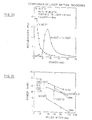
- FIG. 9 shows reflectivity-wavelength curves for six Si/Rh films cn quartz with 25nm Rh covered by 15, 20, 25, 30, 35 and 40nm Si films.
- the reflectivity shows maxima and minima and they vary with film thickness. It is noted that these curves show a much stronger dependence of reflectivity on wavelength than those in FIG. 7.
- the reflectivity-wavelength curve for the annealed sample Si (25nm)/Rh (25nm) for example is shown by the broken line in FIG. 9. Before annealing, the sample showed a reflectivity minimum at ⁇ 6630nm. At this wavelength, which is desirable for writing, a ⁇ R of about 47% is observed.
- More intense laser illumination produced red areas, associated with solid state reaction of the Rh and Si films and formation of a fine grain silicide of undetermined structure and composition.
- FIG. 9 shows the reflectivity of a bi-layei of FIG. 2 for indicated thicknesses of Rh and Si. Note that for a wavelength of 600nm of light frcm a laser beam or the like the reflectance of Curve B is zero. Note the contrast with the RhSi compound curve shown in dotted form. Curve C is for 250A each of Rh and Si and it has a minimum slightly above zero at about 660nm. The curve in FIG. 10 shows slightly different results for Rh nominally 250A and Si 250A after annealing at 700°C for 30 minutes. At the preferred frequency (of a gallium arsenide laser) the difference in reflectivity is 47%. Just above 7000A the difference in reflectivity is very large in percentage terms, nearly infinite according to the data shown.
- FIG. 11 shows the curves of reflectivity percent as a function of wavelength for a thinner 150A thick film of Rh. Thicknesses G, H and J of Si are comparable to those for curves C, D and E in FIG. 9, and it can be seen that the minimum of zero at about 780nm of curve H differs very substantially from the result shown for curve D in FIG. 9. The percentage contrast is much greater also at 810nm. It can be seen that at 600nm a red laser can be used with curve B in Fig.9 and curve G in Fig.11 to achieve extremely large ratios of reflectivity. Thus optimisation will be enhanced by employing curves of this type for the material used for recording.
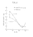
- Fig.12 shows the percentages of reflectivity as a function of Si thickness for the bi-layer of Fig.2 and the silicide of rhodium in the dotted line curve. For these thicknesses, it can be seen that the maximum difference in reflectivity is provided at 150A, for an 800nm laser beam. These thicknesses correspond to those for curve A in Fig.9, but no such data is shown in Fig.11.
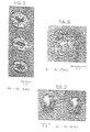
- Fig.13 is of a photograph magnified 30k times of a bright field transmission electron micrograph (TEM) of a mark made by a 5600 Argstrom wavelength laser beam on a cobalt/silicon bi-layer as in Fig.2.
- TEM transmission electron micrograph
- Fig.14 is of a photograph also magnified 30k times of the same mark in the dark field mode.
- the centre (dark in Fig.13) is a thinner laver of amorphous Co Si which has been heated more bv the laser beam than the surrounding area.
- the next oval ring (lighter in Fig.12) is composed of Co x Si y amorphous material which is thicker.
- the dark ring about the light ring in Fig.12 is composed of crystalline CoSi compound material.
- the surrounding grey area is the bi-layer of Co/Si which is in its unexposed state. The optical contrast of the inner oval with the surrounding area is quite sharp as can be seen.
- Rhodium forms similar patterns with two amorphous Rh x Si y inner portions.
- the thinned amorphous centre surrounded by a thicker rim is caused by writing with a level of laser power exceeding the optimum value.
- This pattern indicates the beginning of formation of a hole in the amorphous centre, where material has been driven away towards the rim. Slightly lower levels of power of the laser beam does not lead to a thickened rim around the amorphous centre.
- Fig.15 is of a T EM magnified 20k times which shows three marks made by the same laser on a bi-layer of Au/Si in accordance with Fig.2 where the ratio of Au to Si is 84 atomic percent in the Au/Si Bi-layer according to a microprobe analysis.
- the centre of the mark is black where the amorphous material is located.
- Around the amorphous material is a ring of crystalline material.
- Fig.17 is a TEM magnified 20k times of a set of marks made in a medium rich in silicon with 87 atomic percent Si and 13 atomic percent Au.
- the centre has been transformed to the amorphous Au Si material x y with the formation of a bubble of material lifted slightly off the substrate as can be seen by the curvature shading at the lower portion of the photographs of the TEMs.
- the crystalline Au Si compound At the periphery is the crystalline Au Si compound and then the surrounding material is shown.
- Application of a greater period or intensity of laser radiation would cause the central bubble of amorphous material either to thin out or to collapse so that the contrast would be better, similarly to the marks in Fig.15.
- the percentage of optical reflectivity of an Si Au bilayer on an SiO 2 spacer layer on an Al mirror layer on a substrate is shown in Fig.18 for various wavelengths.
- Fig.19 shows a Pd/Si chart of reflectivity fraction as a function of wavelength for a 250A base of Pd coated with six different thicknesses of Si.
- curve N For the 8100A GaAs laser, curve N with 300A thickness of Si will provide the greatest contrast, as can be seen.
- Curves L and M have similar minima for lasers in the 5500A and 6700A ranges.
- Fig.20 shows a comparison of laser writing with tellurium (Te) and a FIG. 14 shows a comparison of laser writing with tellurium (Te) and a Rh.Si bi-layer as a function of power.
- a power level below 30mw of a 8741A wavelength laser is required to make a mark on Te.
- the curve drops rapidly to below 10% reflectivity at 20mw power.
- the reflectivity of the bi-layer is low u p to about 20mw of power and peaks at about 37mw of power reading about 45%. What happens with a Te coated medium is that the laser begins to open holes in the Te immediately.
- the first portion of the curve involves the reflectivity change as Rh and Si mix, and as the reflectivity curve for Rh/Si declines above 40mw of power, holes open in the Rh/Si bi-layer.
- Te there is ablation whereas with the bi-layer of Rh/Si there is no ablation below 30mw, but there is instead a reaction of the two layers, at least until the power level is raised high enough to form holes in the material.
- Table III shows the writing power required to produce a mark with various media most of which are thin film bi-layers in accordance with this invention. Comparison with tellurium is made in the last two entries.
- Palladium covered with silicon requires only a short pulse as do Si/Pd and Rh/Si with the power required being less for Pd/Si, increasing for Rh/Si and greatest for Si/Pd because of the reflectivity of the metal Pd being so much higher than Si in the other two cases.
- Mo/Si the power required to form silicides is only 35mw with a longer pulse of 500ns.
- the power is the same but the pulse length increases to 800ns and for Nb/Si, the power is less at 30mw but the time of the pulse required is greater at 1000ns.
- the power levels required are low, but the length of the pulse is 1000ns, which makes the writing speed slow.
- Au/Ge and Te are included in the table for the purpose of comparison. The power required to open a hole is higher and the pulse length is long.
- Rh/Si provides a high data rate of only 100ns pulse length. While Te is superior on this basis, requiring lower power or shorter pulses, it loses in comparison of lifetime. In terms of lifetimes, the life of Rh is extremely long, Pt is long, Pd less long, and Te extremely short.
- FIG. 20 shows the curves of power required to write on various materials on different substrates. Except for the Te on PMMA curve, the rest of the curves are Rh/Si in thicknesses of 300A/300A and 150A/300A. It can be seen that polyester and PMMA appear to require less energy. The glass suffers in this comparison from the fact that the thickness of the Rh was greater.
- Te less power to provide a mark for a given pulse width, and is far more easy to mark than Rh/Si 150A/300A on the PMMA substrate. Also, as is obvious, less power is required as the pulse width increases. The slope of the curve seems to be greater for PMMA. For a short pulse width of less than 50ns, the polyester requires a lower power.
- Single pulse laser writing on Pd/Si, Co/Si and V/Si bi-layer films with a thickness varying from 300 to 500A showed that films on AZ resist on glass can be written with 0.88w whereas on glass no effect was observed with less than 1.2w.
- the N 2 pumped dye laser had a single pulse width of 5ns and was focused to a spot size of about 1 ⁇ m. Scanning microscopy showed that although at >2.5w holes were blown in the film, intermediate to no effect at ⁇ 0.8w the film shows shallow mounds in the centre of the spot with one or more concentric grooves towards the edge.
- Silicide formation is quite systematic. It always starts with metal rich silicides and progresses towards the silicon rich silicides. Near noble metal silicides are easier to form, i.e., form at low temperatures, than silicides of refractory metals. For specific transition metals, Table IV shows the sequence of formation. The lower the acti- 7 ation energy shown, the easier it is to form the silicide.
- the medium 10 comprises a substrate 12 which can be transparent or opaque depending upon the application for which the medium is to be used.
- a layer 14 of a first material is deposited upon the substrate 12 and this first material is preferably a metal.
- a layer 16 of a second material is deposited upon the first layer 14, and the second material is preferably a metal or a semiconductor.
- a passivating layer 18 is deposited upon the medium 1G to protect the materials comprising layers 14 and 16 from corrosion due to exposure to environmental factors during the lifetime of the medium.
- Information is recorded in medium 10 by directing an energy beam of suitable power level to the medium.
- the energy beam is absorbed in layer 16 and, to a lesser extent in layer 14, to cause localized heating in the adjoining areas of layers 14 and 16 of sufficient magnitude to produce a change in the optical properties of the materials comprising layers 14 and 16.
- the energy beam such as beam Bl shown in the drawing, is preferably directed toward the surface 11 of the medium to produce a recorded spot 19.
- beam B2 could as well be utilized to produce recorded spot 19 by directing beam B2 through substrate 12.
- the materials comprising layers 14 and 16 would be interchanged.
- FIG. 25 shows what is believed to occur during recording with localized melting in layers 14 and 16 due to heating by the beam B1 and a mixing of the component materials across their interface as shown by the small arrows.
- FIGS. 26 and 27 show the recorded area 19 after recording.
- the configuration of the medium 20 is very similar to the FIG. 22 embodiment with substrate 22 composed of any substrate material suitable for a recording medium.
- Layer 24 is deposited upon the substrate and this layer is preferably a metal.
- Layer 26 is deposited upon layer 24, and layer 26 is preferably a semiconductor. Note that in this case, a separate passivation layer is not required since the semiconductor layer 26 also serves as a passivation layer.
- Suitable semiconductor materials can be chosen from germanium or silicon.
- FIG. 24 shows a further configuration of a medium 30 comprising a suitable substrate 32, a first recording layer 34 which preferably comprises a metal, a second recording layer 36 which preferably comprises either a metal or a semiconductcr, and a thick passivation layer 38.
- passivation layer 38 can be several thousand Angstroms thick and may comprise poly(methylmethacrylate) (PMMA) or other suitable polymeric materials.
- PMMA poly(methylmethacrylate)
- the passivation layer 38 is sufficiently thick so that its surface 40 is not in the same focal plane as the recording layers 34, 36. This construction has the advantage that minor amounts of dust or other contaminants on the surface 40 of the medium 30 do not adversely affect either recording or playback operations.
- the preferred medium comprises a 200 Angstrom thick layer of Al deposited on a PMMA substrate, followed by deposition on the Al of a 230 Angstrom thick layer of Ge, and a passivating layer of Si0 2 substantially as shown in FIG. 1.
- This medium had spots recorded with a dye laser at a wavelength of 5800 Angstrom, using a pulse width of 10 nanoseconds. No attempt was made to optimize the laser power requirements, but the tests indicated a power level requirement no greater than that required for a standard Si0 2 overcoated Te Optical Recording Material.
- the recorded spots when examined by SEM, showed flat recorded spots along with flat background. The contrast was sufficiently high that reliable reading could be accomplished.
- a similar medium was fabricated using a 200 Angstrom thick layer of Al deposited on a PMMA substrate.
- a layer of Si 350 Angstrom thick was deposited on the Al layer and overcoated with a passivating layer of MgO.
- the writing energy for a 1000 Angstrom thickness of MgO was slightly higher than that for Ge-Al.
- the contrast was also less, but the contrast could be varied with the thickness of the MgO layer.
- the SEM showed a slightly domed spot, but no material was removed, and the reflectivity within the spot was consistently higher than outside the spot.
- a medium was made with a 300 Angstrom thickness Pb layer deposited on a PMMA substrate. A 320 Angstrom thick layer of Sn was then deposited over the Pb followed by a 1000 Angstrom thick passivating layer of SiO 2 . The writing energy to form a recorded spot was a factor of 2 greater than for the Ge-Al medium. The constrast was also lower than that for other media tested. The SEM shows a segmented effect in the film with individual segments being fully “written” or else completely “unwritten". While the medium was regarded as unsuitable for some applications, it could be used in a digital form of recording.
- a medium which may require the lowest laser power comprises a 300 Angstrom thick layer of In deposited on a PMMA substrate, overcoated with a 230 Angstrom thick Ge layer and a passivating layer of Si0 2 . Based on the melting point of this combination of materials, the laser power required should be the lowest, however, this has not yet been established by actual tests.
Landscapes
- Chemical & Material Sciences (AREA)
- Inorganic Chemistry (AREA)
- Optical Record Carriers And Manufacture Thereof (AREA)
- Thermal Transfer Or Thermal Recording In General (AREA)
- Read Only Memory (AREA)
- Heat Sensitive Colour Forming Recording (AREA)
Abstract
Description
- This invention relates to optical storage media and methods of recording' thereon.
- In optical storage of data, use of lasers to record data optically has been employed in forming pits in a recording medium to change the reflectivity of the medium. Pits are formed by evaporation, melting, or ablation. Recording can be employed which uses changes of reflectivity or transmission of light to indicate data. Bell and Spong in "Anti-reflection Structures for Optical Recording" IEEE Journal of Quantum Electronics QE14, No. 7, 487495 (July 1978) describes on page 489 a monolayer structure of bismuth, titanium, or rhodium. A bi-layer anti-reflection structure can include Al or a dielectric stack of TiO2/MgF2/TiO2. Organic dyes such as fluorescein have been used in such recording media. Another structure mentioned on page 493 of Bell and Spong is an Al reflector covered with a dielectric spacer and a Ti absorbing layer. Numerous optical recording variations have been proposed but they will not all be discussed here. The problem with the above alternatives is that they will not provide long-life storage of information without employing strong laser beams.
- US 3,959,799 teaches read-only storage media consisting of adjacent thin layers of two or more materials which react, upon heating, to form a reaction product different from those of the reactants. More specifically, a storage medium is described which comprises alternate aluminium and selenium layers which react to form a transparent product, A12Se3, by locally heating the layers such as by the employment of a laser pulse.
- U.S. patent 4,069,487 suggests that a laser optical storage system can be used in which a metallic element (selected from Pt, Rh, Au, Ag, Pd, Ir, Cr, Mo, Ta, Zn, Cu, Al, In, Sn, Pb, and Bi Col. 8) can be layered with a non-metallic layer such as a chalcogen compound, inorganic oxide or resin (dye or pigment). The chalcogens include a chalcogen element such as S, Se and Te.
- Widely publicised optical storage materials such as Te and Te-based alloys suffer from relatively short lifetimes primarily because of corrosion of these very thin films on the order of 100 atomic-layers. An archival storage system is required to provide data integrity for a period of at least 10 years in an ordinary environment.
- U.S. 4,000,492 shows thin metal films upon a transparent substrate with a first layer of Bi, In or Sn and a second layer closer to the laser source composed of BiS3r SbS3 and Se.
- There have been known in the art optical recording media which result in the removal of material in regions approximating the diffraction-limited spot size of the recording laser. While high contrast between the written and unwritten areas has generally been achieved, the signal-to-noise ratio has been limited in some cases by edge effects around the periphery of the spots, which cause some scattering of the read beam. Additionally, these media, such as those based on Te and Te alloys, suffer from corrosion effects.
- There have also been known a number of other optical recording media and other means of marking these media; however, the ones of these media which have achieved long-life recording of information have required higher laser power levels than is desirable, i.e., higher than that achieved with Te-based alloys.
- An object,of this invention is to provide an optical storage medium which provides extremely high densities of machine readable data.
- Another object of this invention is to provide archival level storage of data with assurance of both clarity of the data and long-term retention of the data.
- Another object of this invention is to provide an optical recording medium which is capable of storing information in response to a laser beam of acceptable power level and which will also have sufficient lifetime for archival storage purposes.
- According to this invention there is provided an optical storage medium including first and second adjacent layers of different materials which, upon marking with an energy beam, form a marked area having optical properties different from the optical properties of the unmarked areas, said first layer comprising a metal; and said second layer comprising a metal or a semiconductor.
- Preferably the semiconductor of the second layer is silicon, and the metal of the first layer is a transition metal.
- The metals preferred of the first layer include the group VB, VIB, VIIB and VIII elements on the periodic chart, plus Mg and Au. The more advantageous metals include V, Nb, Ta, Cr, Mo, W, Mn, Fe, Co, Rh, Ni, Pd, Pt and Au. Those metals which are most effective include Pd, Pt, Cr, Ta, Rh, V and Co.
- The layer in contact with the silicon layer is preferably of a material which can be locally combined or reacted with silicon by local heating to produce a silicide which is an optically distinguishable mark and which is stable.
- The silicon layer may be the outer layer so that the other layer is not exposed by prolonged storage in standard ranges of ambient environmental conditions such as those found in offices and conventional manufacturing environments.
- The materials of the first and second layers can endothermically combine or react together to form the optically distinguishable marked area. The metals are selected from the group comprising Al, Au, Pb, and Sn and the semiconductors are chosen from the group comprising Ge and Si. The endothermically formed marked area comprises an alloy or mixture of the materials.
- The materials disclosed here produce an optical recording medium capable of recording information at high recording density with acceptable laser power levels and which has lifetime characteristics suitable for archival storage purposes.
- According to another aspect of the invention, there is provided a method of recording data for subsequent optical readout, in which an energy beam is used to apply local heating to first and second adjacent layers, one of which layers is of metal and the other of which layers is of metal or semiconductor which can be locally combined or reacted with the metal of the first layer by local heating, to produce an optically distinguishable mark and which is stable.
- The relatively short lifetime associated with the conventional Te-based alloys due to corrosion is increased to at least 10 years by use of the materials disclosed herein.
- The scope of the invention is defined by the appended claims; and how it can be carried into effect is hereinafter particularly described with reference to the accompanying drawings, in which :-
- FIGURE 1 is a schematic drawing of one embodiment of optical storage medium in accordance with this invention;
- FIGURE 2 is a similar drawing of another embodiment;
- FIGURE 3 is a sectional schematic drawing of a multilayer optical storage medium according to this invention;
- FIGURES 4 and 5 show differences in reflectivity between Pd and Pd2Si and a black reference;
- FIGURE 6 is a schematic drawing of an arrangement by which reflectivity was measured;
- FIGURE 7 shows percentage of reflectivity versus wavelength for two bi-layers in accordance with this invention;
- FIGURE 8 shows glancing-incidence Seeman-Bohlin x-ray diffraction spectra of an Rh/Si film as a function of annealing time;
- FIGURE 9 shows percentage of reflectivity versus wavelength for Rh/Si bi-layers;
- FIGURE 10 shows reflectivity versus wavelength for Rh/Si before and after annealing;
- FIGURE 11 shows percentage of reflectivity versus wavelength for Rh/Si bi-layers;
- FIGURE 12 shows percent of reflectivity versus silicon thickness for an Rh/Si bi-layer;
- FIGURE 13 is a TEM bright field photograph of a mark written by a laser on a Co/Si bi-layer;
- FIGURE 14 is a photograph in the dark field mode of the same mark as in FIG. 13;
- FIGURES 15 to 17 show TEM photographs of marks on Au/Si bi-layers of varying compositions;
- FIGURE 18 shows reflectivity versus wavelength for a Si/Au bi-layer;
- FIGURE 19 shows reflectivity versus wavelength curves for various Si/Pd bi-layers;
- FIGURE 20 shows reflectivity percentage versus laser power for Te and Rh/Si bi-layers;
- FIGURE 21 shows power versus pulse width as a function for various substrates carrying Te or Rh/Si bi-layers.
- FIGURE 22 is a side view of another embodiment of an optical recording medium in accordance with this invention;
- FIGURE 23 is a side view of an alternate embodiment of the optical recording medium in accordance with this invention;
- FIGURE 24 is a side view of a further embodiment of the optical recording medium in accordance with this invention;
- FIGURE 25 is a side view partially in section showing the recording of a marked area in accordance with this invention;
- FIGURE 26 is a side view partially in section showing the recorded marked area of the recording medium in accordance with this invention; and
- FIGURE 27 is a plan view of the recording medium showing the recorded marked area of FIG. 5.
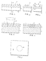
- Figure 1 is a schematic representation of an optical storage medium according to one embodiment of the invention. The medium comprises substrate Sl which can be transparent or opaque, depending upon the application for which the medium is to be employed. Upon the substrate is a layer in the form of a thin film of silicon (Si). Upon the silicon layer is another layer in the form of a thin film of a metal Ml which when heated sufficiently (by means such as laser beam Bl) can combine with the silicon to provide a mark readable by a sensor, such as an optical senscr of the type employed in optical recording devices. The data recorded can be stored with such high density that visual inspection is possible only with optical magnification. In general, the metal film Ml upon the top of the silicon provides high reflectivity of light. About 65% and more of beam Bl is reflected. In general, high writing energy is required to heat the metal Ml sufficiently to form a mark because of the high level of reflectivity. In addition, the metal film Ml is exposed to ambient conditions which will tend to shorten the life of the medium because of oxidation due to humidity causing oxygen to react with the metal. Such oxidation will spoil the reflectivity of the metal thereby destroying the contrast in reflectivity required for storing data. However, if the substrate Sl is transparent, then the silicon can be exposed to the energy from a source, such as a laser beam B2, which strikes the silicon which has a low value of reflectivity less than or equal to about 5%. This leads to a low writing energy because little heating is required to raf .e the silicon to a high enough temperature to heat the interface between the metal Ml and the silicon to the temperature required to form a mark. In addition, in the case of exposure of the medium through the substrate, the metal Ml can be covered with a protective layer to inhibit degradation of the metal film.
- The preferred metals Ml for use in the metal layer are rhodium, cobalt, palladium, platinum, chromium, tantalum and vanadium. In general, the group VB metals V, Nb and Ta are all useful in this connection. Group VIB, VIIB, VIII metals, Mg and Au are all applicable in particular among all other metals. Specifically, the group VIB metals are Cr, Mo, and W. The group VIIB metals are Mn, Tc, and Re. The group VIII metals are Fe, Co, Ni, Ru, Rh, Pd, Os, Ir and Pt. Au is, of course, the nearest neighbour of Pt on the periodic chart although it is a group IB metal.
- Another embodiment of the invention (Fig.2) is similar to that of Fig.l with substrate S2 being composed of any substrate material suitable for a recording medium. A metal layer M2 in the form of a thin film is deposited upon the substrate S2 first. Next, a thin film silicon layer is deposited upon the metal M2. In this case, it is preferred to write upon the upper surface of the medium with laser beam B (or alternative radiation other than a laser beam) rather than with a beam B4 passing through the substrate to heat the metal directly, as with beam B1 in Fig.l. Another advantage of the structure of Fig.2 is that the silicon layer on the metal layer M2 provides a passivation layer, per se, requiring no additional film to protect the metal layer M2, because the substrate protects the lower surface.
- In another embodiment of the invention, a multi-layer optical storage medium (Fig.3) has a substrate S3 which may be a recording disk for high deneray storage. The next layer is a reflective mirror layer MR, which may be of titanium. or other metal which is highly reflective and which is sufficaiently refractory. Ti has a melting point of 1668°C so that it is suitable for use without degradation. Upon mirror layer MR is deposited a dielectric spacer layer SP which is preferably composed of a material, such as SiO2, which is of an appropriate thickness to maximize the wavelength of the laser beam B5 which is directed upon a pair of thin films A and 5 which are respectively a metal layer and a silicon layer. The materials of films A and B are interchangeable, so that the metal may be on top as film A (as in Fig.1) or below as film B (as in Fig.2). In either case, the light which passes through the films A and B is reflected back to heat the upper films so as to increase the efficiency of the laser beam B5, thereby requiring less energy from beam B5 to write data at a given point. Again, the placement of the silicon as the upper film A should enhance the efficiency of the data recording function.
- Films of silicide (a compound of metal and silicon) have been widely studied for their applications in micro-electronic devices as contact materials.
- K N Tu and J W Mayer,
chapter 10 in "Thin Films - Interdiffusion and Reactions" Ed. by J M Poate, K N Tu and J W Mayer, Wiley-Interscience, New York (1978). - In forming silicide contacts by reacting a deposited metallic film with Si, a large optical contrast between the silicide and the unreacted metallic film has often been observed. C J Kircher, Solid State Electron. 14,507 (1971).
- The present invention arises from a study of optical contrasts. For example, Fig.4 shows the dark spot of a Pd2Si contact 0.025mm in diameter in an etched hole on an oxidized Si wafer surrounded by a much preghter pd area. Fig.5 shows differences in reflectivity between these and a black reference. These suggested that silicide films could be considered as potential materials for archival optical storage, provided that the contrast between the silicide and the metal (or Si) in reflection is large enough for the application. Other crucial requirements for materials in arhival optical storage are a long lifetime, over 10 years at room temperature and non-toxicity. Findings on reflectivity change and stability of silicide films for the storage application are discussed below.
- The difference in optical reflectivity between metallic films and their silicides formed on Si wavers was measured. Several transition metal films of thicknesses shown in Table I were prepared by E-beam deposition in a vacuum chamber of 13.33224 x 10⁻⁶pa (10-7 torr) onto [100] oriented Si wafers of about 32mm in diameter, as shown in Fig.6. Optical reflectivity (R ) shown in Table I is the value measured at λ= 643.7nm (Kr laser), with θ the angle of incidence of light upon the film being zero.
- These films were then annealed at proper conditions to form silicides, and reflectivity values were measured again as shown in Table I. As can be seen, most pairs of a metal and its silicide show a difference in reflectivity ΔR greater than 30%. The largest difference observed is that between Pd and Pd2Si, about 53%. The difference has been found to vary with the wavelength of light used, and Fig.7 shows variations in optical reflectivity of films of Pd, Pt, Pd-Pd2Si and Pt-PtSi pairs measured on Si wafers as a function of wavelength of light used. In the wavelength range shown in Fig.7 ΔR between Pd and Pd2Si shows a larger change than that between Pt and PtSi.
-

- Pd2Si and PtsI are two compounds which have many desirable properties including stability and optical contrast. Pd2Si and PtSi are both formed when local spots are heated by a laser beam during recording. Fig.l shows a schematic drawing of a structure in which the readout is done by reflection. A substrate of Si or a thin film of Si is deposited onto a suitable substrate by means of vacuum deposition technique or CVD process. A thin layer of Pd or Pt film is then deposited onto the Si film, where the thickness of Pd and Pt may range from 20 nm to 60 nm (200Å to 600Å).
- The percentage of optical reflectivity of these films ranges from 80% for Pd to 84% for Pt at a wavelength of interest, say 640nm (6400Å). The spectra shown in Fig.7 are for films of 100 nm (1000Å) thickness. Digital information is recorded by local heating of spots with pulsed laser beam by moving the storage film or by scanning the laser beam by moving the storage film or by scanning the laser beam over the stationary storage film. The temperature of the local spots may exceed several hundred degrees Celsius, and this causes the formation of compounds such as pd2Si and PtSi by thermal diffusion or melting. The percentage of optical reflectivity of these compounds is very low, typically less than 40%. For example, at the wavelength of interest, at 640nm (6400Å), the percent of reflectivity is 28% for Pd2Si and 44% for PtSi, as shown in Fig.7 and Table I.

- From P.376, Thin Films -- Interdifussion and Reactions, Ed. by Poate, Tu, and Mayer, John Wiley & Sons (1978).
- As to the lifetime of such devices, consider the diffusion of Pd into Si at room temperature. Taking 1.4 eV as the average activation energy, the diffusion distance in 10 years turns out to be 0.55nm.
- Although not shown in Fig.l, a dielectric thin film in the thickness range of 100nm (1000Å) may be deposited over the Pd surface as an anti-reflection coating which may also serve as a passivation layer, to enhance the corrosion resistance.
- In an optical storage disk (Fig.3) the active layers A and B may be Rh on Si or Si on Rh and can be deposited on a SiO dielectric spacer layer SP. The thickness of each active layer, typically less than 15nm, is chosen such that there is maximum contrast between the laser written spot and the unreacted background.
- When a thin film of rhodium is in contact with a layer of silicon and heated to a temperature higher than 400°C, reaction takes place at the interface that forms RhSi. Below 377°C no reaction was observed to take place (D. J. Coe, E. H. Rhoderick, P. H. Gerzon, and A. W. Ginsley, "Silicide Formation in Rh-Si Schottky barrier diodes", Inst. of Phys. Conf. Ser. 22, p. 74, 1974), and this makes the Rh system more attractive for long-term storage applications.
- The active layers A and B (Si+Rh or Rh+Si) are on a Ti mirror (40 to 50 nm thick) separated by an SiO2 dielectric spacer (90 to 100 nm thick).
- Information is stored by local heating of spots with a laser beam where heating causes reaction of Rh and Si to form silicides. The difference in optical reflectivity before and after formation of silicide is sufficient to give an adequate contrast ratio for readback. For example, the reflectivity of a Rh film of 200 nm (2000A) on Si at the wavelength of interest (643.7 nm) is typically 67%, and this reduces to 37% after formation of RhSi by annealing at 500°C for 60 minutes.
- The main advantage of this is that it avoids the difficult process of ablating perfectly circular holes as used in conventional low-temperature storage materials such as Te and Te-based alloys.
- The element Rh is known to be almost corrosion free, and other optical files fabricated with Rh film (with very high laser energy) are certified to be archival by the National Bureau of Standards in the United States.of America. Rhodium offers resistance to atmospheric corrosion of the disk, thus providing a longer lifetime than metals which are more reactive.
- Although a bi-layer structure is shown for the active layer in FIG. 3, any variaition in the structure may be used, for example a trilayer structure of Si-Rh-Si can be employed to optimize the optical properties.
- The lifetime of media is determined largely by degradation of the film caused by corrosion or interfacial diffusion.
- With respect to corrosion, Pt/Si, Rh/Si and Pd/Si films (where the metal is deposited first and the silicon later) are much less easily corroded than conventional storage media such as Te.
- Room temperature lifetime of these bi-layer film structures has to be estimated by an accelerated test and by extrapolation using the known silicide growth rate in thicker films measured at higher temperatures. In the case of 200nm Rh films on Si wafers, the growth of RhSi around 400°C was observed to be diffusion-controlled with an activation energy of 1.9eV. See the following references. D. J. Coe, E. H. Rhoderick, D. H. Gerzon and A. W. Ginsely, in "Metal-Semiconductor Contacts", Conference Series No. 22, Institute of Physics, London 1974; S. Petersson, R. Anderson, J. Dempsey, W. Hammer, F. d'Heurle and S. Laplaca, J. Appl. Phys. 51,373 (1980). By extrapolating it to room temperature, a diffusion-like kinetic constant of 10-31cm2/sec and an estimated growth of RhSi of lnm in a period of 10 years are expected, which practically means no growth of RhSi. However, to check experimentally if an under estimate had been made for the reaction rate in very thin films used here, an accelerated test was performed by annealing the Si/Rh bi-layer films at 150°C for periods of up to 98 days. Fig.8 shows glancing-incidence Seeman-Bohlin x-ray diffraction spectra of a Si (25nm)/Rh (25nm) film as deposited, annealed at 150°C for 49 days and 98 days. The extra reflections in (d) belong to RhSi. The intensity of the reflections in (a) is less than those of (b) and (d) due to shorter counting time. Only after 98 days is some RhSi formation observed; about 30nm of Rh has been transformed to RhSi estimated from the relative intensity change of Rh reflections before and after the annealing. If the reported 1.9eV activation energy is used to estimate the growth of RhSi at 150°C after 98 days, a growth of about lnm of RhSi is obtained, which is quite close to the value measured. It is concluded that the bi- layer film structure of Si/Rh will be stable at room temperature over 10 years. However, the same measurement showed that the bi-layer structure of Si/Pt will be marginally stable though satisfactory and Si/Pd will transform to Pd2Si probably in less than 10 years at room temperature.
- In summary, it has been demonstrated that bi-layer film structure of Si and transition metals are promising materials for archival optical storage. They show a large reflectivity change before and after silicide formation and some of them, such as Si/Rh, have extremely good stability at room temperature. Furthermore, they are non-toxic.
- Although the large ΔR observed is interesting, the thick films used experimentally are not suitable for optical storage application because they require relatively high laser power in writing.
- Much thinner bi-layer thin films of Si/metal have been prepared by consecutive deposition on oxidized Si wafers, fused quartz, and photoresist coated quartz for reflectivity and stability measurements. The bi-layer configuration of Si/metal/substrate of Fig.2 rather than metal/Si/substrate of Fig.l was selected because of lower reflectivity, lower writing energy, and better surface passivation by the Si. Three near-noble metals, Pd, Pt and Rh were chosen to form the bi-layers because their silicides are easier to form than those of refractory metals.
- This will save power during laser writing, yet it is noted that there is a trade-off in lifetime if the silicide forms very easily. The thickness of either the Si or the metal in the bi-layer structure has been varied in order to investigate the effect of interfacial interference on reflectivity.
- For example, FIG. 9 shows reflectivity-wavelength curves for six Si/Rh films cn quartz with 25nm Rh covered by 15, 20, 25, 30, 35 and 40nm Si films. The reflectivity shows maxima and minima and they vary with film thickness. It is noted that these curves show a much stronger dependence of reflectivity on wavelength than those in FIG. 7. After annealing at 700°C for 30 minutes to form RhSi silicide, the reflectivity-wavelength curve for the annealed sample Si (25nm)/Rh (25nm) for example, is shown by the broken line in FIG. 9. Before annealing, the sample showed a reflectivity minimum at λ~6630nm. At this wavelength, which is desirable for writing, a ΔR of about 47% is observed.
- Laser beam writing on Pt/Si and Rh/Si bi-layer films shows that thermal conductivities of substrates carrying the bi-layer films play an important role in determining power requirements for the write operation. With an argon laser (50% duty cycle), only 0.5 - l.Omw is needed to write 10µm diameter spots with Rh/Si films on 400A thick Si3N4 window structures; 10 - 20mw is needed for films on glass substrates, and more than 35mw is needed for films on higher thermal conductivity Si substrates. For comparison, 2-3mw is typically necessary to write on Te films on glass substrates. Laser written spots on the Pt/Si and Rh/Si bi-layer films can also be described in terms of their apparent colours when viewed by back reflection of white light, or in terms of the local change in reflectivity for monochromatic light, e.g., argon laser illumination λ =514.nNm found that blue, red, and yellow spots written on Rh/Si bi-layers, had reflectivity changes of<'5% (blue)-37% (red) and +68% (yellow), in comparison with adjacent unwritten areas. Transmission electren microscopy and diffraction were used to determine the structural redifications responsible for the various colour and reflectivity changes. For Rh/Si films on thin Si3N4 windows, blue areas were asscorated simply with grain growth of the metallic Rh. More intense laser illumination produced red areas, associated with solid state reaction of the Rh and Si films and formation of a fine grain silicide of undetermined structure and composition. Still higher laser powers produced yellow areas, with larger crystals of orthorhombic Rh5Si3 and of an unidentified cubic phase (a = 4.72A).
- FIG. 9 shows the reflectivity of a bi-layei of FIG. 2 for indicated thicknesses of Rh and Si. Note that for a wavelength of 600nm of light frcm a laser beam or the like the reflectance of Curve B is zero. Note the contrast with the RhSi compound curve shown in dotted form. Curve C is for 250A each of Rh and Si and it has a minimum slightly above zero at about 660nm. The curve in FIG. 10 shows slightly different results for Rh nominally 250A and
Si 250A after annealing at 700°C for 30 minutes. At the preferred frequency (of a gallium arsenide laser) the difference in reflectivity is 47%. Just above 7000A the difference in reflectivity is very large in percentage terms, nearly infinite according to the data shown. - FIG. 11 shows the curves of reflectivity percent as a function of wavelength for a thinner 150A thick film of Rh. Thicknesses G, H and J of Si are comparable to those for curves C, D and E in FIG. 9, and it can be seen that the minimum of zero at about 780nm of curve H differs very substantially from the result shown for curve D in FIG. 9. The percentage contrast is much greater also at 810nm. It can be seen that at 600nm a red laser can be used with curve B in Fig.9 and curve G in Fig.11 to achieve extremely large ratios of reflectivity. Thus optimisation will be enhanced by employing curves of this type for the material used for recording.
- Fig.12 shows the percentages of reflectivity as a function of Si thickness for the bi-layer of Fig.2 and the silicide of rhodium in the dotted line curve. For these thicknesses, it can be seen that the maximum difference in reflectivity is provided at 150A, for an 800nm laser beam. These thicknesses correspond to those for curve A in Fig.9, but no such data is shown in Fig.11.
- Fig.13 is of a photograph magnified 30k times of a bright field transmission electron micrograph (TEM) of a mark made by a 5600 Argstrom wavelength laser beam on a cobalt/silicon bi-layer as in Fig.2.
- Fig.14 is of a photograph also magnified 30k times of the same mark in the dark field mode. In the centre (dark in Fig.13) is a thinner laver of amorphous Co Si which has been heated more bv the laser beam than the surrounding area. The next oval ring (lighter in Fig.12) is composed of CoxSiy amorphous material which is thicker. The dark ring about the light ring in Fig.12 is composed of crystalline CoSi compound material. The surrounding grey area is the bi-layer of Co/Si which is in its unexposed state. The optical contrast of the inner oval with the surrounding area is quite sharp as can be seen.
- Rhodium forms similar patterns with two amorphous RhxSiy inner portions. The thinned amorphous centre surrounded by a thicker rim is caused by writing with a level of laser power exceeding the optimum value. This pattern indicates the beginning of formation of a hole in the amorphous centre, where material has been driven away towards the rim. Slightly lower levels of power of the laser beam does not lead to a thickened rim around the amorphous centre.
- Fig.15 is of a TEM magnified 20k times which shows three marks made by the same laser on a bi-layer of Au/Si in accordance with Fig.2 where the ratio of Au to Si is 84 atomic percent in the Au/Si Bi-layer according to a microprobe analysis. The centre of the mark is black where the amorphous material is located. Around the amorphous material is a ring of crystalline material.
- In the TEM photograph magnified 30k times of Fig.16, the bi-layer is 79 atomic percent silicon and 21 atomic percent gold. The same laser beam applied to this gold rich material produced a crystalline mark which has poor characteristics for an optical record because of the low contrast between the mark and its surroundings. Fig.17 is a TEM magnified 20k times of a set of marks made in a medium rich in silicon with 87 atomic percent Si and 13 atomic percent Au. In this case the centre has been transformed to the amorphous Au Si material x y with the formation of a bubble of material lifted slightly off the substrate as can be seen by the curvature shading at the lower portion of the photographs of the TEMs. At the periphery is the crystalline Au Si compound and then the surrounding material is shown. Application of a greater period or intensity of laser radiation would cause the central bubble of amorphous material either to thin out or to collapse so that the contrast would be better, similarly to the marks in Fig.15.
- For optical reflectivity it does not matter whether the mixed bi-layer in the mark is amorphous or crystalline.
- The percentage of optical reflectivity of an Si Au bilayer on an SiO2 spacer layer on an Al mirror layer on a substrate is shown in Fig.18 for various wavelengths.
- Fig.19 shows a Pd/Si chart of reflectivity fraction as a function of wavelength for a 250A base of Pd coated with six different thicknesses of Si. For the 8100A GaAs laser, curve N with 300A thickness of Si will provide the greatest contrast, as can be seen. Curves L and M have similar minima for lasers in the 5500A and 6700A ranges.
- Fig.20 shows a comparison of laser writing with tellurium (Te) and a FIG. 14 shows a comparison of laser writing with tellurium (Te) and a Rh.Si bi-layer as a function of power. A power level below 30mw of a 8741A wavelength laser is required to make a mark on Te. The curve drops rapidly to below 10% reflectivity at 20mw power. For rhodium/silicon bi-layers of 300A each, the reflectivity of the bi-layer is low up to about 20mw of power and peaks at about 37mw of power reading about 45%. What happens with a Te coated medium is that the laser begins to open holes in the Te immediately. With the bi-layer, the first portion of the curve involves the reflectivity change as Rh and Si mix, and as the reflectivity curve for Rh/Si declines above 40mw of power, holes open in the Rh/Si bi-layer. In addition, with Te there is ablation whereas with the bi-layer of Rh/Si there is no ablation below 30mw, but there is instead a reaction of the two layers, at least until the power level is raised high enough to form holes in the material.
- Table III shows the writing power required to produce a mark with various media most of which are thin film bi-layers in accordance with this invention. Comparison with tellurium is made in the last two entries. Palladium covered with silicon requires only a short pulse as do Si/Pd and Rh/Si with the power required being less for Pd/Si, increasing for Rh/Si and greatest for Si/Pd because of the reflectivity of the metal Pd being so much higher than Si in the other two cases. With Mo/Si, the power required to form silicides is only 35mw with a longer pulse of 500ns. For Zr/Si, the power is the same but the pulse length increases to 800ns and for Nb/Si, the power is less at 30mw but the time of the pulse required is greater at 1000ns. For Si/Co and Co/Si the power levels required are low, but the length of the pulse is 1000ns, which makes the writing speed slow. Au/Ge and Te are included in the table for the purpose of comparison. The power required to open a hole is higher and the pulse length is long.

- In summary, Rh/Si provides a high data rate of only 100ns pulse length. While Te is superior on this basis, requiring lower power or shorter pulses, it loses in comparison of lifetime. In terms of lifetimes, the life of Rh is extremely long, Pt is long, Pd less long, and Te extremely short.
- FIG. 20 shows the curves of power required to write on various materials on different substrates. Except for the Te on PMMA curve, the rest of the curves are Rh/Si in thicknesses of 300A/300A and 150A/300A. It can be seen that polyester and PMMA appear to require less energy. The glass suffers in this comparison from the fact that the thickness of the Rh was greater.
- Clearly, Te less power to provide a mark for a given pulse width, and is far more easy to mark than Rh/
Si 150A/300A on the PMMA substrate. Also, as is obvious, less power is required as the pulse width increases. The slope of the curve seems to be greater for PMMA. For a short pulse width of less than 50ns, the polyester requires a lower power. - Single pulse laser writing on Pd/Si, Co/Si and V/Si bi-layer films with a thickness varying from 300 to 500A, showed that films on AZ resist on glass can be written with 0.88w whereas on glass no effect was observed with less than 1.2w. The N2 pumped dye laser had a single pulse width of 5ns and was focused to a spot size of about 1µm. Scanning microscopy showed that although at >2.5w holes were blown in the film, intermediate to no effect at <0.8w the film shows shallow mounds in the centre of the spot with one or more concentric grooves towards the edge.
- In the cases of Pd/Si and Co/Si, the centre was found to be amorphous but not so in V/Si. All the spots showed silicide formation. No major difference was found in the size of spots with 2 or 10 consecutive pulses into the same area. These results have demonstrated the writing ability of laser on silicide forming films.

- Silicide formation is quite systematic. It always starts with metal rich silicides and progresses towards the silicon rich silicides. Near noble metal silicides are easier to form, i.e., form at low temperatures, than silicides of refractory metals. For specific transition metals, Table IV shows the sequence of formation. The lower the acti- 7ation energy shown, the easier it is to form the silicide.
- In the embodiment of the recording medium, according to the invention shown in FIG. 22, the medium 10 comprises a
substrate 12 which can be transparent or opaque depending upon the application for which the medium is to be used. Alayer 14 of a first material is deposited upon thesubstrate 12 and this first material is preferably a metal. Alayer 16 of a second material is deposited upon thefirst layer 14, and the second material is preferably a metal or a semiconductor. Apassivating layer 18 is deposited upon the medium 1G to protect thematerials comprising layers - Information is recorded in
medium 10 by directing an energy beam of suitable power level to the medium. The energy beam is absorbed inlayer 16 and, to a lesser extent inlayer 14, to cause localized heating in the adjoining areas oflayers materials comprising layers - The energy beam, such as beam Bl shown in the drawing, is preferably directed toward the
surface 11 of the medium to produce a recordedspot 19. However, should thesubstrate 12 be transparent to the radiation in the energy beam, beam B2 could as well be utilized to produce recordedspot 19 by directing beam B2 throughsubstrate 12. In this case, thematerials comprising layers - The exact nature of the change that takes place is not fully understood since the heating takes place in a time which is in the order of 20 nanoseconds. FIG. 25 shows what is believed to occur during recording with localized melting in
layers area 19 after recording. - Examination of the recorded
area 19 with a Scanning Electron Microscope (SEM) shows a flat recorded spot on a flat background, and no noticeable change in composition from inside to outside the recorded spot. The optical changes are believed to result from either an alloying or mixture of the twomaterials comprising layers - Referring to FIG. 23, the configuration of the medium 20 is very similar to the FIG. 22 embodiment with substrate 22 composed of any substrate material suitable for a recording medium.
Layer 24 is deposited upon the substrate and this layer is preferably a metal.Layer 26 is deposited uponlayer 24, andlayer 26 is preferably a semiconductor. Note that in this case, a separate passivation layer is not required since thesemiconductor layer 26 also serves as a passivation layer. Suitable semiconductor materials can be chosen from germanium or silicon. - The embodiment of the invention shown in FIG. 24 shows a further configuration of a medium 30 comprising a
suitable substrate 32, a first recording layer 34 which preferably comprises a metal, a second recording layer 36 which preferably comprises either a metal or a semiconductcr, and athick passivation layer 38. In this case,passivation layer 38 can be several thousand Angstroms thick and may comprise poly(methylmethacrylate) (PMMA) or other suitable polymeric materials. In this embodiment, thepassivation layer 38 is sufficiently thick so that itssurface 40 is not in the same focal plane as the recording layers 34, 36. This construction has the advantage that minor amounts of dust or other contaminants on thesurface 40 of the medium 30 do not adversely affect either recording or playback operations. - The preferred medium comprises a 200 Angstrom thick layer of Al deposited on a PMMA substrate, followed by deposition on the Al of a 230 Angstrom thick layer of Ge, and a passivating layer of Si02 substantially as shown in FIG. 1. This medium had spots recorded with a dye laser at a wavelength of 5800 Angstrom, using a pulse width of 10 nanoseconds. No attempt was made to optimize the laser power requirements, but the tests indicated a power level requirement no greater than that required for a standard Si02 overcoated Te Optical Recording Material. The recorded spots, when examined by SEM, showed flat recorded spots along with flat background. The contrast was sufficiently high that reliable reading could be accomplished.
- A similar medium was fabricated using a 200 Angstrom thick layer of Al deposited on a PMMA substrate. A layer of
Si 350 Angstrom thick was deposited on the Al layer and overcoated with a passivating layer of MgO. The writing energy for a 1000 Angstrom thickness of MgO was slightly higher than that for Ge-Al. The contrast was also less, but the contrast could be varied with the thickness of the MgO layer. The SEM showed a slightly domed spot, but no material was removed, and the reflectivity within the spot was consistently higher than outside the spot. - A medium was made with a 300 Angstrom thickness Pb layer deposited on a PMMA substrate. A 320 Angstrom thick layer of Sn was then deposited over the Pb followed by a 1000 Angstrom thick passivating layer of SiO2. The writing energy to form a recorded spot was a factor of 2 greater than for the Ge-Al medium. The constrast was also lower than that for other media tested. The SEM shows a segmented effect in the film with individual segments being fully "written" or else completely "unwritten". While the medium was regarded as unsuitable for some applications, it could be used in a digital form of recording.
- A medium which may require the lowest laser power comprises a 300 Angstrom thick layer of In deposited on a PMMA substrate, overcoated with a 230 Angstrom thick Ge layer and a passivating layer of Si02. Based on the melting point of this combination of materials, the laser power required should be the lowest, however, this has not yet been established by actual tests.
Claims (14)
Applications Claiming Priority (2)
| Application Number | Priority Date | Filing Date | Title |
|---|---|---|---|
| US27628381A | 1981-06-22 | 1981-06-22 | |
| US276283 | 1981-06-22 |
Publications (3)
| Publication Number | Publication Date |
|---|---|
| EP0068801A2 true EP0068801A2 (en) | 1983-01-05 |
| EP0068801A3 EP0068801A3 (en) | 1983-05-25 |
| EP0068801B1 EP0068801B1 (en) | 1986-09-10 |
Family
ID=23056010
Family Applications (1)
| Application Number | Title | Priority Date | Filing Date |
|---|---|---|---|
| EP19820303256 Expired EP0068801B1 (en) | 1981-06-22 | 1982-06-22 | Optical storage medium |
Country Status (4)
| Country | Link |
|---|---|
| EP (1) | EP0068801B1 (en) |
| JP (1) | JPS5816890A (en) |
| CA (1) | CA1199404A (en) |
| DE (1) | DE3273164D1 (en) |
Cited By (12)
| Publication number | Priority date | Publication date | Assignee | Title |
|---|---|---|---|---|
| EP0097774A2 (en) * | 1982-06-30 | 1984-01-11 | International Business Machines Corporation | Transducing system |
| EP0132410A2 (en) * | 1983-07-25 | 1985-01-30 | Sony Corporation | Information recording media |
| US4572886A (en) * | 1983-11-03 | 1986-02-25 | Texas Instruments Incorporated | Optical method for integrated circuit bar identification |
| GB2167225A (en) * | 1984-11-21 | 1986-05-21 | Drexler Tech | Data system containing a high capacity optical contrast laser recordable wallet-size plastics card |
| FR2573560A1 (en) * | 1984-11-21 | 1986-05-23 | Drexler Tech | Laser recordable plastic card mfr. method |
| US4633451A (en) * | 1982-06-30 | 1986-12-30 | International Business Machines Corporation | Optical servo for magnetic disks |
| EP0150829B1 (en) * | 1984-01-28 | 1989-03-22 | Kabushiki Kaisha Toshiba | Optical disk |
| EP0377864A2 (en) * | 1989-01-13 | 1990-07-18 | International Business Machines Corporation | Optical storage device |
| EP1359576A2 (en) * | 2002-04-30 | 2003-11-05 | TDK Corporation | Optical recording medium and method for optically recording data on the same |
| EP1367577A1 (en) * | 2002-05-31 | 2003-12-03 | TDK Corporation | Optical recording medium and method for optically recording data in the same |
| US7141289B2 (en) | 2003-08-25 | 2006-11-28 | Tdk Corporation | Optical information recording medium |
| US7157128B2 (en) | 2003-07-23 | 2007-01-02 | Tdk Corporation | Optical information recording medium |
Families Citing this family (1)
| Publication number | Priority date | Publication date | Assignee | Title |
|---|---|---|---|---|
| JP4059714B2 (en) | 2002-07-04 | 2008-03-12 | Tdk株式会社 | Optical recording medium |
Citations (9)
| Publication number | Priority date | Publication date | Assignee | Title |
|---|---|---|---|---|
| DE1574687A1 (en) * | 1968-02-06 | 1970-07-16 | Bosch Gmbh Robert | Recording medium for recording information by means of modulated light beams |
| US3650743A (en) * | 1967-10-06 | 1972-03-21 | Teeg Research Inc | Methods for making lithographic offset plates by means of electromagnetic radiation sensitive elements |
| FR2284163A1 (en) * | 1974-09-09 | 1976-04-02 | Ibm | METHOD AND DEVICE FOR STORING INFORMATION BY REACTIONS TRIGGERED BY MEANS OF A LASER BEAM |
| DE2558529A1 (en) * | 1974-12-28 | 1976-07-08 | Fuji Photo Film Co Ltd | Recording material contg. metal and cpd. giving sharp copies - with high energy radiation esp. laser beams, without environmental pollution |
| FR2367273A1 (en) * | 1976-10-08 | 1978-05-05 | Bosch Gmbh Robert | RECORDING MEDIA |
| GB2007860A (en) * | 1977-11-04 | 1979-05-23 | Asahi Chemical Ind | Impaging material and method of producing image thereon |
| GB2026901A (en) * | 1978-06-26 | 1980-02-13 | Fuji Photo Film Co Ltd | Thermal recording elements |
| US4202928A (en) * | 1978-07-24 | 1980-05-13 | Rca Corporation | Updateable optical storage medium |
| FR2460205A1 (en) * | 1979-07-03 | 1981-01-23 | Inst Elektrodinamiki Akademii | Radiation-sensitive recording material - with a metallic layer e.g. of copper or silver and an inorganic layer of arsenic, antimony or bismuth chalcogenide, with an intermediate s |
-
1982
- 1982-03-18 JP JP57041834A patent/JPS5816890A/en active Granted
- 1982-05-21 CA CA000403576A patent/CA1199404A/en not_active Expired
- 1982-06-22 EP EP19820303256 patent/EP0068801B1/en not_active Expired
- 1982-06-22 DE DE8282303256T patent/DE3273164D1/en not_active Expired
Patent Citations (9)
| Publication number | Priority date | Publication date | Assignee | Title |
|---|---|---|---|---|
| US3650743A (en) * | 1967-10-06 | 1972-03-21 | Teeg Research Inc | Methods for making lithographic offset plates by means of electromagnetic radiation sensitive elements |
| DE1574687A1 (en) * | 1968-02-06 | 1970-07-16 | Bosch Gmbh Robert | Recording medium for recording information by means of modulated light beams |
| FR2284163A1 (en) * | 1974-09-09 | 1976-04-02 | Ibm | METHOD AND DEVICE FOR STORING INFORMATION BY REACTIONS TRIGGERED BY MEANS OF A LASER BEAM |
| DE2558529A1 (en) * | 1974-12-28 | 1976-07-08 | Fuji Photo Film Co Ltd | Recording material contg. metal and cpd. giving sharp copies - with high energy radiation esp. laser beams, without environmental pollution |
| FR2367273A1 (en) * | 1976-10-08 | 1978-05-05 | Bosch Gmbh Robert | RECORDING MEDIA |
| GB2007860A (en) * | 1977-11-04 | 1979-05-23 | Asahi Chemical Ind | Impaging material and method of producing image thereon |
| GB2026901A (en) * | 1978-06-26 | 1980-02-13 | Fuji Photo Film Co Ltd | Thermal recording elements |
| US4202928A (en) * | 1978-07-24 | 1980-05-13 | Rca Corporation | Updateable optical storage medium |
| FR2460205A1 (en) * | 1979-07-03 | 1981-01-23 | Inst Elektrodinamiki Akademii | Radiation-sensitive recording material - with a metallic layer e.g. of copper or silver and an inorganic layer of arsenic, antimony or bismuth chalcogenide, with an intermediate s |
Cited By (16)
| Publication number | Priority date | Publication date | Assignee | Title |
|---|---|---|---|---|
| US4633451A (en) * | 1982-06-30 | 1986-12-30 | International Business Machines Corporation | Optical servo for magnetic disks |
| EP0097774A3 (en) * | 1982-06-30 | 1986-02-05 | International Business Machines Corporation | Transducing system |
| EP0097774A2 (en) * | 1982-06-30 | 1984-01-11 | International Business Machines Corporation | Transducing system |
| EP0132410A2 (en) * | 1983-07-25 | 1985-01-30 | Sony Corporation | Information recording media |
| EP0132410A3 (en) * | 1983-07-25 | 1985-10-02 | Sony Corporation | Information recording media |
| US4572886A (en) * | 1983-11-03 | 1986-02-25 | Texas Instruments Incorporated | Optical method for integrated circuit bar identification |
| EP0150829B1 (en) * | 1984-01-28 | 1989-03-22 | Kabushiki Kaisha Toshiba | Optical disk |
| FR2573560A1 (en) * | 1984-11-21 | 1986-05-23 | Drexler Tech | Laser recordable plastic card mfr. method |
| GB2167225A (en) * | 1984-11-21 | 1986-05-21 | Drexler Tech | Data system containing a high capacity optical contrast laser recordable wallet-size plastics card |
| EP0377864A2 (en) * | 1989-01-13 | 1990-07-18 | International Business Machines Corporation | Optical storage device |
| EP0377864A3 (en) * | 1989-01-13 | 1991-01-16 | International Business Machines Corporation | Optical storage device |
| EP1359576A2 (en) * | 2002-04-30 | 2003-11-05 | TDK Corporation | Optical recording medium and method for optically recording data on the same |
| EP1359576A3 (en) * | 2002-04-30 | 2005-03-16 | TDK Corporation | Optical recording medium and method for optically recording data on the same |
| EP1367577A1 (en) * | 2002-05-31 | 2003-12-03 | TDK Corporation | Optical recording medium and method for optically recording data in the same |
| US7157128B2 (en) | 2003-07-23 | 2007-01-02 | Tdk Corporation | Optical information recording medium |
| US7141289B2 (en) | 2003-08-25 | 2006-11-28 | Tdk Corporation | Optical information recording medium |
Also Published As
| Publication number | Publication date |
|---|---|
| DE3273164D1 (en) | 1986-10-16 |
| CA1199404A (en) | 1986-01-14 |
| EP0068801B1 (en) | 1986-09-10 |
| EP0068801A3 (en) | 1983-05-25 |
| JPS5816890A (en) | 1983-01-31 |
| JPH0247355B2 (en) | 1990-10-19 |
Similar Documents
| Publication | Publication Date | Title |
|---|---|---|
| EP1293974B1 (en) | Optical information recording medium | |
| KR100658538B1 (en) | Optical recording/reproducing method and optical recording medium | |
| EP0068801A2 (en) | Optical storage medium | |
| US6592958B2 (en) | Optical recording medium and sputtering target for fabricating the recording medium | |
| EP1609139B1 (en) | Recording medium having super-resolution near-field structure and method and apparatus for reproducing the same | |
| JP3088168B2 (en) | Optical recording medium and manufacturing method thereof | |
| JP2001273671A (en) | Thin film structure for optical recording medium | |
| KR20110061618A (en) | Data storage media containing carbon and metal layers | |
| JP3268157B2 (en) | Optical recording medium | |
| US7161894B2 (en) | Optical recording article | |
| EP0700037A1 (en) | Information recording medium | |
| EP0237181B1 (en) | Information recording medium and information write/read method using the same | |
| EP1372148B1 (en) | Optical recording medium, process for manufacturing the same and optical recording process using the same | |
| TWI299864B (en) | High density readable only optical disc and method of preparing the same | |
| US7758941B2 (en) | Optical data storage medium with super resolution layer | |
| JP2004171631A (en) | Optical recording medium | |
| JP4541420B2 (en) | Optical data storage medium with semi-reflective tin-tellurium alloy layer | |
| TWI478160B (en) | Data storage media containing carbon and metal layers and method for preparing optical information medium | |
| JPH0327975B2 (en) | ||
| JPS63299982A (en) | Optical recording medium and recording method using the same | |
| JP3137093B2 (en) | Phase change recording medium | |
| JPH10255324A (en) | Phase transition type recording medium | |
| JPH05159363A (en) | Optical recording medium | |
| JP2001283477A (en) | Initialization method for optical recording medium | |
| US20090176048A1 (en) | AgSb recording thin film for the inorganic write-once optical disc and the manufacturing method |
Legal Events
| Date | Code | Title | Description |
|---|---|---|---|
| PUAI | Public reference made under article 153(3) epc to a published international application that has entered the european phase |
Free format text: ORIGINAL CODE: 0009012 |
|
| AK | Designated contracting states |
Designated state(s): DE FR GB IT |
|
| PUAL | Search report despatched |
Free format text: ORIGINAL CODE: 0009013 |
|
| AK | Designated contracting states |
Designated state(s): DE FR GB IT |
|
| 17P | Request for examination filed |
Effective date: 19830420 |
|
| GRAA | (expected) grant |
Free format text: ORIGINAL CODE: 0009210 |
|
| AK | Designated contracting states |
Kind code of ref document: B1 Designated state(s): DE FR GB IT |
|
| REF | Corresponds to: |
Ref document number: 3273164 Country of ref document: DE Date of ref document: 19861016 |
|
| ET | Fr: translation filed | ||
| ITF | It: translation for a ep patent filed | ||
| PLBE | No opposition filed within time limit |
Free format text: ORIGINAL CODE: 0009261 |
|
| STAA | Information on the status of an ep patent application or granted ep patent |
Free format text: STATUS: NO OPPOSITION FILED WITHIN TIME LIMIT |
|
| 26N | No opposition filed | ||
| ITTA | It: last paid annual fee | ||
| PGFP | Annual fee paid to national office [announced via postgrant information from national office to epo] |
Ref country code: GB Payment date: 19920506 Year of fee payment: 11 |
|
| PGFP | Annual fee paid to national office [announced via postgrant information from national office to epo] |
Ref country code: FR Payment date: 19920601 Year of fee payment: 11 |
|
| PGFP | Annual fee paid to national office [announced via postgrant information from national office to epo] |
Ref country code: DE Payment date: 19920619 Year of fee payment: 11 |
|
| PG25 | Lapsed in a contracting state [announced via postgrant information from national office to epo] |
Ref country code: GB Effective date: 19930622 |
|
| GBPC | Gb: european patent ceased through non-payment of renewal fee |
Effective date: 19930622 |
|
| PG25 | Lapsed in a contracting state [announced via postgrant information from national office to epo] |
Ref country code: FR Effective date: 19940228 |
|
| PG25 | Lapsed in a contracting state [announced via postgrant information from national office to epo] |
Ref country code: DE Effective date: 19940301 |
|
| REG | Reference to a national code |
Ref country code: FR Ref legal event code: ST |