EP0067716A1 - Induction motor control system - Google Patents
Induction motor control system Download PDFInfo
- Publication number
- EP0067716A1 EP0067716A1 EP82303119A EP82303119A EP0067716A1 EP 0067716 A1 EP0067716 A1 EP 0067716A1 EP 82303119 A EP82303119 A EP 82303119A EP 82303119 A EP82303119 A EP 82303119A EP 0067716 A1 EP0067716 A1 EP 0067716A1
- Authority
- EP
- European Patent Office
- Prior art keywords
- current
- regenerative
- transistor inverter
- motor
- voltage
- Prior art date
- Legal status (The legal status is an assumption and is not a legal conclusion. Google has not performed a legal analysis and makes no representation as to the accuracy of the status listed.)
- Granted
Links
- 230000006698 induction Effects 0.000 title claims abstract description 35
- 230000001172 regenerating effect Effects 0.000 claims abstract description 63
- 239000003990 capacitor Substances 0.000 claims abstract description 23
- 238000009499 grossing Methods 0.000 claims abstract description 23
- 230000008929 regeneration Effects 0.000 claims description 16
- 238000011069 regeneration method Methods 0.000 claims description 16
- 238000001514 detection method Methods 0.000 claims description 8
- 238000012544 monitoring process Methods 0.000 abstract description 9
- 238000010304 firing Methods 0.000 description 14
- 238000000034 method Methods 0.000 description 11
- 230000016507 interphase Effects 0.000 description 8
- 238000010586 diagram Methods 0.000 description 7
- 238000010276 construction Methods 0.000 description 4
- 230000007423 decrease Effects 0.000 description 3
- 230000006378 damage Effects 0.000 description 2
- 230000001360 synchronised effect Effects 0.000 description 2
- 230000001960 triggered effect Effects 0.000 description 2
- 230000015572 biosynthetic process Effects 0.000 description 1
- 230000002708 enhancing effect Effects 0.000 description 1
- 230000002401 inhibitory effect Effects 0.000 description 1
- 238000004519 manufacturing process Methods 0.000 description 1
- 238000009877 rendering Methods 0.000 description 1
- 230000003252 repetitive effect Effects 0.000 description 1
- 230000002441 reversible effect Effects 0.000 description 1
- 230000002123 temporal effect Effects 0.000 description 1
Images


Classifications
-
- H—ELECTRICITY
- H02—GENERATION; CONVERSION OR DISTRIBUTION OF ELECTRIC POWER
- H02P—CONTROL OR REGULATION OF ELECTRIC MOTORS, ELECTRIC GENERATORS OR DYNAMO-ELECTRIC CONVERTERS; CONTROLLING TRANSFORMERS, REACTORS OR CHOKE COILS
- H02P3/00—Arrangements for stopping or slowing electric motors, generators, or dynamo-electric converters
- H02P3/06—Arrangements for stopping or slowing electric motors, generators, or dynamo-electric converters for stopping or slowing an individual dynamo-electric motor or dynamo-electric converter
- H02P3/18—Arrangements for stopping or slowing electric motors, generators, or dynamo-electric converters for stopping or slowing an individual dynamo-electric motor or dynamo-electric converter for stopping or slowing an ac motor
-
- H—ELECTRICITY
- H02—GENERATION; CONVERSION OR DISTRIBUTION OF ELECTRIC POWER
- H02P—CONTROL OR REGULATION OF ELECTRIC MOTORS, ELECTRIC GENERATORS OR DYNAMO-ELECTRIC CONVERTERS; CONTROLLING TRANSFORMERS, REACTORS OR CHOKE COILS
- H02P23/00—Arrangements or methods for the control of AC motors characterised by a control method other than vector control
- H02P23/06—Controlling the motor in four quadrants
-
- H—ELECTRICITY
- H02—GENERATION; CONVERSION OR DISTRIBUTION OF ELECTRIC POWER
- H02P—CONTROL OR REGULATION OF ELECTRIC MOTORS, ELECTRIC GENERATORS OR DYNAMO-ELECTRIC CONVERTERS; CONTROLLING TRANSFORMERS, REACTORS OR CHOKE COILS
- H02P27/00—Arrangements or methods for the control of AC motors characterised by the kind of supply voltage
- H02P27/04—Arrangements or methods for the control of AC motors characterised by the kind of supply voltage using variable-frequency supply voltage, e.g. inverter or converter supply voltage
- H02P27/06—Arrangements or methods for the control of AC motors characterised by the kind of supply voltage using variable-frequency supply voltage, e.g. inverter or converter supply voltage using dc to ac converters or inverters
Definitions
- This invention relates to an induction motor control system and, more particularly, to an induction motor control system which, barring accidents, enables an induction motor to continue running even when there is a large increase in regenerative energy, and which performs regenerative braking with excellent efficiency.
- Induction motors are employed in a variety of industrial fields and can be applied to a variety of loads. Some induction motors undergo rapid and frequent increases and decreases in speed, while in others there are positive and negative changes in load torque, as when raising and lowering an object in the manner of a hoist. Thus there in a requirement that an induction motor functioning as a driving source be operated so as to generate a positive torque as well as a braking torque.
- a method of controlling the operation of induction motors which has recently come into fairly widespread use employs a variable voltage-variable frequency inverter. While no major problems are encountered in this method when operating the motor in the driving mode, one difficulty which does arise is the manner of dealing with the rotational energy possessed by the rotor of the motor when operating the motor in the braking mode at the time of a reduction in speed.
- Two exemplary methods of dealing with this rotational energy have been adopted in the prior art.
- the flow of current to the induction motor is interrupted for braking to permit the motor to slow down naturally owing to mechanical loss attributed to the load.
- the slip which occurs at deceleration is suitably controlled and is allowed to dissipate within the motor.
- the first method requires too much time to achieve the speed reduction and has a very poor control response, while the second method causes the motor to overheat to such an extent that it cannot endure frequent increases and decreases in speed.
- Another method which can be mentioned is one in which the rotational energy of the rotor is dissipated by allowing a smoothing capacitor, inserted in the inverter circuitry mentioned above, to charge until the charged voltage exceeds a specified value, whereupon the capacitor is discharged through a braking resistor connected in parallel with the inverter circuit, thereby to dissipate the energy.
- This method is disadvantageous, however, in that it may lead to destruction of the apparatus if the smoothing capacitor is charged to an excessively large voltage, and in that costs are raised since the braking resistor increases in size and expense in accordance with the size of the machine to be driven by the motor.
- the method is undesirable in terms of enhancing efficiency because of the fact that the braking energy is wasted in the form of thermal loss.
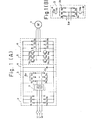
- Fig. 1(A) is a circuit diagram showing an induction motor operation control apparatus of the regenerative braking type according to the prior art.
- the apparatus includes a three-phase induction motor 1, a full-wave rectifier 2 constructed of diodes D 1 through D 6 for rectifying the U, V and W phases of the AC input power, a regenerative circuit 3 having a thyristor bridge comprising thyristors 51 through S 6 , a smoothing circuit 4 having a smoothing capacitor C 1 , a variable voltage-variable frequency inverter 5 composed of transistors TA 1 through TA 6 , a rectifier 6 comprising diodes D 1 ' through D 6 ', and a step-up transformer for boosting the power source voltage.
- the commanded speed is reduced in magnitude so that the synchronous speed becomes smaller than the motor speed, giving rise to a negative slip condition. Accordingly, the motor operates in the regenerative braking region, with the result that the voltage induced in the motor is rectified by the rectifier 6, thereby raising the voltage on the DC line side.
- the smoothing capacitor C 1 in order for it to exhibit the smoothing function, is charged to a voltage that is 1.3 to 1.4 times the AC power supply voltage even when the motor is operating in the normal driving mode. Nevertheless, when the induction motor is operated in the regenerative region, the smoothing capacitor C 1 is charged to, and held at, an even higher voltage.
- the voltage to which the capacitor C 1 is charged is raised to approximately 290 volts.
- the firing of the regenerative thyristor bridge 3 is controlled under such conditions, commutation cannot take place and regenerative operation becomes impossible because the AC power supply voltage is lower than the voltage on the side of the DC line, even though it may be possible to fire the thyristors.
- the thyristors S 1 through S 6 are forward biased, a thyristor which has already fired cannot be turned off, making regeneration impossible.
- the step-up transformer 7 is inserted between the AC power supply and the thyristor bridge 3, and the circuitry is arranged in such a manner that there will always be intervals in which the AC power supply voltage is higher than the voltage on the DC line side, thereby assuring commutation of the thyristors S 1 through S 6 and enabling operation in the regenerative braking region.
- the apparatus that employs this system is large in size and high in price owing to the need for the step-up transformer 7 of a large capacity.
- Fig. 1(B) the Inventors have previously proposed a system, illustrated in Fig. 1(B), which dispenses with the step-up transformer.
- two switching transistors TR 1 , TR2 are connected in series with a thyristor bridge 31 and are turned off when any of the thyristors S 1 through S 6 commutes. This switching action severs the thyristors S 1 through S 6 from the lines A, B, overcoming the forward biased state so that commutation is assured.
- the voltage of the smoothing capacitor C 1 (referred to as a DC link voltage) is monitored and an alarm signal is issued with said voltage reaches a dangerous level, which is preset.
- the alarm signal completely halts the operation of the regenerative circuit 3 and transistor inverter 6, with the result that the motor can no longer run from that point onward. More specifically, in the conventional system a large amount of regenerative energy causes the DC link voltage to exceed a preset value, from which point operation of the motor ceases completely. In many cases, however, the preset voltage is exceeded not because of a system failure or the like, but merely because the regenerative energy has become too large.
- the present invention relates to an induction motor control system, and more particularly to the control and protection of an induction motor during regenerative braking.
- An object of the present invention is to provide a novel induction motor control system in which, when the regenerative energy takes on a large value and causes the DC link voltage or the motor current to enlarge and exceed a first preset value, only the transistor inverter is temporarily disabled to allow the energy, stored in the smoothing capacitor, to dissipate through the regenerative circuit, without the motor coming to a complete stop, whereby regenerative braking control of the motor can be resumed after the magnitude of the regenerative energy drops below the first preset value.
- Another object of the present invention is to provide an induction motor control system in which, when the DC link voltage or motor current exceeds a second preset value, this is regarded as indicating a failure or accident, in response to which an alarm signal is immediately produced and motor operation brought to a complete halt.
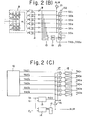
- Reference numeral 11 denotes a regeneration control circuit which generates control signals SG 1 through SG 6 for controlling the firing of thyristors S 1 through S 6 constituting the thyristor bridge 31, and which further generates on/off control signals TRB 1 , TRB 2 for controlling the switching transistors TR 1 , TR 2 . More specifically, the regeneration control circuit 11 receives the three-phase alternating voltage of the power supply and is adapted to fire the thyristors connected to the two phases that develop the largest interphase voltage.
- the regeneration control circuit 11 generates the firing control signals SG 1 through SG 6 , which are pulse pairs spaced apart by T/6 (where T is the period of the alternating current), a pair of the pulses being produced in successive fashion at intervals of T/6, as shown in Fig. 3(B), and further produces the control signals TRB 1 , TRB 2 in sync with commutation timing.
- T/6 the period of the alternating current
- TRB 1 , TRB 2 in sync with commutation timing.
- the construction of the regeneration control circuit 11 is such that when the DC link voltage V C exceeds a second preset value E 2' described below, an alarm signal ALM goes to logical "1", and the firing control signals SG 1 through SG 6 , as well as the control signal TRB 1 , are no longer produced.
- reference numeral 12 denotes an inverter control circuit for controlling the timing of each of the transistors TA 1 through TA 6 constituting the transistor inverter 5.
- the inverter control circuit 12 produces transistor drive signals TAD 1 ' through TAD 6 ' in response to which the transistor inverter 5 supplies the induction motor 1 with a three-phase primary voltage of a frequency and effective value in conformance with the error or deviation between a commanded rotational speed and the actual rotational speed of the motor.
- a monitoring circuit 13 is provided to monitor the terminal voltage (DC link voltage) V c of the smoothing capacitor C 1 .
- the monitoring circuit 13 compares the magnitudes of its two inputs, namely the DC link voltage V C and a reference voltage E 1 , namely a first preset value, and produces a signal RGS whose level is low (logical "0") when the condition V C ⁇ E 1 holds, and high (logical "1") when the condition V C ⁇ E 1 holds.
- a flip-flop 16 initially in the reset state, is set and produces the alarm signal ALM when signal TGS goes high.
- the set output of the flip-flop 15 is applied to a NOT gate 16, whose is output is connected to a group of AND gates 17.
- the AND gates 17 take the AND among the signal RGS, each of the transistor drive signals TAD 1 ' through TAD 6 ', and a signal * ALM, which is the inverse of the alarm signal ALM.
- the outputs of the AND gates 17 are connected to respective amplifiers 18 for producing drive signals TAD 1 through TAD 6 , respectively.
- each phase of the AC power supply is rectified into a direct current by the rectifier 2.
- the transistor inverter 5 converts the direct current into an alternating current of a prescribed frequency and voltage which is applied to the induction motor 1 to bring the motor speed into agreement with the commanded speed.
- the output frequency of the inverter 5 is capable of being varied by adjusting the repetition frequency of the drive signals TAD through TAD 6 for driving the transistors TA 1 through TA 6 constituting the inverter, and the output voltage of the inverter is capable of being varied by adjusting the conduction time of the transistors TA 1 through TA 6 .
- the induction motor starts to operate in the region of negative slip S, that is, in a regenerative braking region, since the rotational speed of the running motor is greater than the synchronous speed.
- the output of the motor consequently is rectified by the rectifier 6 and raises the voltage on the DC line side. If the motor is operating at an AC power supply voltage of 200 volts, then the voltage at the terminals of the smoothing capacitor C 1 will be raised to approximately 290 volts.
- the switching transistors TR 1 , TR 2 are connected in series with the thyristor group of the regenerative circuit 3 and are rendered conductive during regenerative operation, and momentarily non-conductive at the same time when any of the thyristors S 1 through S 6 is to commute, thereby interrupting the flow of current to the thyristors.
- the transistors TR 1 , TR 2 are rendered conductive again upon taking into account the time during which the thyristors are completely extinguished. Even if the voltage on the DC line side should happen to be higher than the AC voltage of the power supply, therefore, the regenerative current I R will always be fed back to the power supply without any of the thyristors experiencing commutation failure.
- numeral 8 denotes one of the two sections constituting a photocoupler, the other section being made up of such elements as a group of photo-transistors P 1 " through P 6 ", which will be described below.
- the photocoupler 8 includes elements such as light-emitting diodes P 1 ' through P 6 ' and diodes D 1 " through D 6 ", these being connected in the form of a bridge circuit whose AC input side receives the three-phase AC power for the motor, namely the U, V and W phases, in a phase relationship which corresponds to that of the respective thyristors in the thyristor bridge of the regenerative circuit 3.
- the diodes D 1 " through D 6 " serve also to protect the circuit against reverse voltages.
- P 1 " through P 6 " designate photo-transistors or the like, as mentioned above. The arrangement is such that when light-emitting diode P, emits light in response to an inflow of current, the element P 1 ", serving as a light receptor, is rendered conductive upon intercepting the emitted light.
- the output terminal of each element P 1 " through P 6 " is provided with an inverter for inverting the output signal.
- the output signals from all of the inverters 9 are applied to an OR circuit 10 whose output is in turn coupled to a first monostable multivibrator 19 for generating negative pulses of a fixed duration.
- a second multivibrator 20 responds to the output of the first monostable multivibrator 19 to produce pulses of a fixed duration.
- AND gates 22 take the AND between the outputs of the respective inverters 9 and the output of the second monostable multivibrator 20 and are the same in number as the inverters 9.
- the outputs of the AND gates 22 are gating signals SG 1 through SG 6 , namely the firing control signals mentioned earlier, and are applied to the gates of the corresponding thyristors 5 1 through S 6 that form the regenerative thyristor bridge 3.
- the pulses produced by the first monostable multivibrator 19 are base signals TRB 1 , TRB 2 , namely the aforementioned control signals, and are applied simultaneously to the switching transistors TR 1 , TR 2 connected in series with the thyristor group in the thyristor bridge 3.
- the input side of the bridge circuit 8, comprising the elements P,' through P 6 ' such as the light-emitting diodes for constructing a photocoupler, is connected to the U, V and W-phases of the motor driving source.
- the bridge circuit 8 receives the same interphase voltages as the regenerative thyristor bridge 3 so that, from among the thyristors constituting the thyristor bridge 3, it is possible to detect the particular thyristor corresponding to that phase in which firing must be executed for regenerative action.
- Fig. 3(A) For a better understanding of this operation, reference will be had to Fig. 3(A).
- Sinusoidal interphase voltages U-V, V-W, W-U are impressed upon the corresponding phase input terminals of the bridge that forms the photocoupler.
- a current flows only into those light-emitting diodes that receive the largest interphase voltage of the interphase voltages that are applied, said diodes responding by emitting light for the duration of the current flow.
- the light-emitting diodes P 1 ' through P 6 ' are excited in succession in accordance with the temporal variation of the interphase voltages.
- the other photocoupler section namely the section consisting of photo-transistors P 1 " through P 6 " serving as the light receptors, is so arranged as to intercept the light from the light-emitting diodes.
- the corresponding photo-transistor intercepts the light and is rendered conductive, its collector potential going to zero volts and remaining there for as long as the element continues to receive light.
- the outputs of the photo-transistors are illustrated by the waveforms P 1 through P 6 in Fig. 3(A). These signals are inverted to produce signals P 1 through P 6 by means of the inverters 9 connected to the output of each photo-transistor. The inverted signals are applied to one input terminal of each of the corresponding AND gates 22, and to the input side of the OR gate 10.
- the OR gate 10 delivers pulses successively to the monostable multivibrator 19, a pulse being produced by the OR gate each time a pulse in the signals P 1 through P 6 arrives.
- the monostable multivibrator 19 is triggered by the leading edge of each received pulse and is rendered conductive for a fixed period of time only, after which the output of the multivibrator returns to its original state, this operation continuing in repetitive fashion to produce the pulse train shown by M 1 in Fig. 3(A).
- the pulse train has a potential of zero volts for intervals of about 0.5 milliseconds (conduction interval) and is applied to the bases of the switching transistors TR 1 , TR 2 connected in series with the regenerative thyristor bridge, thereby serving to drive the base potentials of the transistors to zero volts to render the transistors non-conductive.
- the pulse train M 1 is applied to the second monostable multivibrator 20 which is triggered to produce the pulse train illustrated by M 2 is Fig. 3(A).
- the pulses are positive pulses having a width of approximately 10 microseconds, and they are timed by the leading edge of each pulse in signal M 1 , that is, each time the signal M 1 returns to its original potential.
- the positive (i.e., logical "1") pulses in pulse train M 2 are applied to each of the AND gates 22.
- the AND gates 22 take the logical AND between the signals P 1 through P 6 , from the inverters 9, and the output pulses M 2 from the second monostable multivibrator 20, thereby producing the firing signals SG 1 through SG 6 which are delivered to the respective gates of the thyristors S 1 through S 6 that construct the regenerative thyristor bridge.
- the phase relationship among the signals SG 1 through SG 6 shown in Fig. 3(B), is of course govened by the output signals P 1 through P 6 of the photocoupler.
- the zero-potential pulses are re-applied to the switching transistors TR 1 , TR 2 to again render them non-conductive, thereby temporarily turning off all of the transistors in the regenerative thyristor bridge 3 once again.
- the switching transistors are driven into conduction again, and firing signals are applied to the thyristors S 1 , S 6 simultaneously.
- a regenerative current flows from the U-phase into the W-phase. This operation continues in similar fashion.
- all of the thyristors are turned off by rendering both switching trnasistors TR 1 , TR 2 non-conductive by applying the zero-potential pulses thereto prior to the commutation of the thyristors and, in successive fashion, the firing signals SG 3 , SG 6 are applied to the thyristors S 2 , S 6 , the firing signals SG 3 , SG 2 are applied to thyristors S 3 , S 2 , and the firing signals SG 5 , SG 2 are applied to the thyristors S 5 , S 2 .
- a regenerative current can be supplied to the two phases of the AC power supply that exhibit the largest interphase voltage.
- Commutation can take place in a reliable manner since the thyristors are turned off temporarily prior to the arrival of the firing signals owing to the fact that the current is interrupted without fail by means of the switching transistors TR 1 , TR 2 .
- the conductive states of thyristors S 1 through S 6 , as well as the waveform of the regenerative current IR , are illustrated by S 1 through S 6 and by I R , respectively, in Fig. 3(B).
- V C is the terminal voltage of the smoothing capacitor C 1 , namely the DC link voltage, V AC the effective value of the power supply voltage, and r 1 , r 2 the magnitudes of the resistors R 1 , R 2 , respectively, connected in series with the switching transistors TR 1 , TR 2 .
- the DC link voltage V C is compared against the reference voltage V r in monitoring circuit 13, as described earlier.
- the magnitude of the reference voltage E 1 is decided upon considering the size of the DC link voltage that would give rise to the maximum allowable current with respect to the switching transistors TR 1 , TR 2 . If the regenerative energy increases to such an extent that V C ⁇ E holds, then the output signal RGS of monitoring circuit 13 will be logical "0". As a result, the outputs of all AND gates 17 will be logical "0", sending all of the drive signals TAD through TAD 6 to logical "0". This cuts off all of the transistors TA 1 through TA 6 in the transistor inverter 5, whereby the inverter ceases to function. When this occurs, the regenerative energy cannot be returned to the power supply.
- the energy stored in the smoothing capacitor C 1 is returned to the power supply through the regenerative circuit 3, so that the terminal voltage V C gradually decreases to establish the condition V c ⁇ E 1 .
- the signal RGS goes to logical "1", restoring the transistor inverter 5 to the operable state so that the regenerative energy may once again be returned to the power supply.
- the foregoing operations are repeated, with either the regenerative energy being returned to the power supply or the transistor inverter 5 being temporarily disabled (during which time the energy stored in the smoothing capacitor C 1 is dissipated), in accordance with the magnitudes of V C and E 1 .
- the monitoring circuit 14 is comparing the DC link voltage V c with the second preset value E 2 , which is greater than the first preset value E 1 .
- the size of the second preset value E 2 is decided upon taking into consideration how large the DC link voltage may become in the event of a failure or accident.
- the monitoring circuit 14 which responds by producing the signal TGS (logical "1"), whereby flip-flop 15 is placed and held in the set state so that the alarm signal ALM is raised to the high level.
- TGS logical "1"
- the inverting action of the transistor inverter 5 is completely inhibited.
- the alarm signal is coupled also to a display unit to give an indication of the failure.
- the alarm signal (logical "1") is applied to the regeneration control circuit 11, the firing control signals SG 1 through SG 6 are no longer produced, thereby inhibiting the regeneration action of the regenerative circuit 3.
- an alternative method of halting the production of the signals SG 1 through SG 6 would be to take the logical AND between the signal * AL M and these signals.
- the result is that the induction motor comes to a complete stop. When the cause of the failure or accident has been removed, motor operation can be restored by resetting the flip-flop 15.
- the motor current can be used instead of the DC link voltage. That is, first and second current detection levels I 1 , I 2 (I 1 ⁇ 1 2 ) can be preset, with the inverting action of the transistor inverter being halted temporarily when the motor current I c exceeds the level I 1 . When I 2 is exceeded, the alarm signal would be generated to disable both the transistor inverter and the regenerative circuit, thereby halting motor operation.
- a current transformer or the like may be used to sense the motor current.
- control of induction motor operation can be continued, without bringing the motor to a complete stop, even when the DC link voltage V C or motor current I C exceeds the first preset value E 1 or I i owing to a comparatively large amount of regenerative energy.
- V c or I C should exceed the second preset value E 2 or 1 2 because of a system failure or accident, then motor operation can be halted to protect the elements constituting the regenerative circuit and transistor inverter. Accordingly, motor operation almost never comes to a halt, enabling control to be effected in a highly efficient and reliable manner.
Landscapes
- Engineering & Computer Science (AREA)
- Power Engineering (AREA)
- Stopping Of Electric Motors (AREA)
- Control Of Ac Motors In General (AREA)
Abstract
Description
- This invention relates to an induction motor control system and, more particularly, to an induction motor control system which, barring accidents, enables an induction motor to continue running even when there is a large increase in regenerative energy, and which performs regenerative braking with excellent efficiency.
- Induction motors are employed in a variety of industrial fields and can be applied to a variety of loads. Some induction motors undergo rapid and frequent increases and decreases in speed, while in others there are positive and negative changes in load torque, as when raising and lowering an object in the manner of a hoist. Thus there in a requirement that an induction motor functioning as a driving source be operated so as to generate a positive torque as well as a braking torque.
- A method of controlling the operation of induction motors which has recently come into fairly widespread use employs a variable voltage-variable frequency inverter. While no major problems are encountered in this method when operating the motor in the driving mode, one difficulty which does arise is the manner of dealing with the rotational energy possessed by the rotor of the motor when operating the motor in the braking mode at the time of a reduction in speed. Two exemplary methods of dealing with this rotational energy have been adopted in the prior art. In one method, the flow of current to the induction motor is interrupted for braking to permit the motor to slow down naturally owing to mechanical loss attributed to the load. In the other method, the slip which occurs at deceleration is suitably controlled and is allowed to dissipate within the motor. The first method, however, requires too much time to achieve the speed reduction and has a very poor control response, while the second method causes the motor to overheat to such an extent that it cannot endure frequent increases and decreases in speed.
- Another method which can be mentioned is one in which the rotational energy of the rotor is dissipated by allowing a smoothing capacitor, inserted in the inverter circuitry mentioned above, to charge until the charged voltage exceeds a specified value, whereupon the capacitor is discharged through a braking resistor connected in parallel with the inverter circuit, thereby to dissipate the energy. This method is disadvantageous, however, in that it may lead to destruction of the apparatus if the smoothing capacitor is charged to an excessively large voltage, and in that costs are raised since the braking resistor increases in size and expense in accordance with the size of the machine to be driven by the motor. Moreover, the method is undesirable in terms of enhancing efficiency because of the fact that the braking energy is wasted in the form of thermal loss.
- Regenerative braking systems, as shown in Figs. 1(A) and 1(B), have been proposed in an effort to improve upon the foregoing arrangements.
- Fig. 1(A) is a circuit diagram showing an induction motor operation control apparatus of the regenerative braking type according to the prior art. The apparatus includes a three-
phase induction motor 1, a full-wave rectifier 2 constructed of diodes D1 through D6 for rectifying the U, V and W phases of the AC input power, aregenerative circuit 3 having a thyristor bridge comprising thyristors 51 through S6, asmoothing circuit 4 having a smoothing capacitor C1, a variable voltage-variable frequency inverter 5 composed of transistors TA1 through TA6, arectifier 6 comprising diodes D1' through D6', and a step-up transformer for boosting the power source voltage. - To control the
induction motor 1 with this conventional arrangement, for example, to decelerate the motor, the commanded speed is reduced in magnitude so that the synchronous speed becomes smaller than the motor speed, giving rise to a negative slip condition. Accordingly, the motor operates in the regenerative braking region, with the result that the voltage induced in the motor is rectified by therectifier 6, thereby raising the voltage on the DC line side. The smoothing capacitor C1, in order for it to exhibit the smoothing function, is charged to a voltage that is 1.3 to 1.4 times the AC power supply voltage even when the motor is operating in the normal driving mode. Nevertheless, when the induction motor is operated in the regenerative region, the smoothing capacitor C1 is charged to, and held at, an even higher voltage. For example, if the AC power supply voltage is 200 volts, the voltage to which the capacitor C1 is charged is raised to approximately 290 volts. When the firing of theregenerative thyristor bridge 3 is controlled under such conditions, commutation cannot take place and regenerative operation becomes impossible because the AC power supply voltage is lower than the voltage on the side of the DC line, even though it may be possible to fire the thyristors. In other words, since the thyristors S1 through S6 are forward biased, a thyristor which has already fired cannot be turned off, making regeneration impossible. To avoid this problem, the step-up transformer 7 is inserted between the AC power supply and thethyristor bridge 3, and the circuitry is arranged in such a manner that there will always be intervals in which the AC power supply voltage is higher than the voltage on the DC line side, thereby assuring commutation of the thyristors S1 through S6 and enabling operation in the regenerative braking region. However, the apparatus that employs this system is large in size and high in price owing to the need for the step-up transformer 7 of a large capacity. - In view of the foregoing drawback, the Inventors have previously proposed a system, illustrated in Fig. 1(B), which dispenses with the step-up transformer. In the proposed system, two switching transistors TR1, TR2are connected in series with a
thyristor bridge 31 and are turned off when any of the thyristors S1 through S6 commutes. This switching action severs the thyristors S1 through S6 from the lines A, B, overcoming the forward biased state so that commutation is assured. - While the previously proposed system is extremely effective, it does not take into account a situation where the voltage of the smoothing capacitor C1 (Fig. 1(A) ) may rise owing to a substantial increase in regenerative energy. That is, when the regenerative energy becomes large in magnitude, the voltage developed by the smoothing capacitor C- rises and there is a gradual increase in the regenerative current IR. This can damage the switching transistors TR1, TR2 or the thyristors S1 through S6 if the regenerative current IR exceeds an allowable limit. When such an arrangement is applied to the system of Fig. 1(A), the voltage of the smoothing capacitor C1 (referred to as a DC link voltage) is monitored and an alarm signal is issued with said voltage reaches a dangerous level, which is preset. The alarm signal completely halts the operation of the
regenerative circuit 3 andtransistor inverter 6, with the result that the motor can no longer run from that point onward. More specifically, in the conventional system a large amount of regenerative energy causes the DC link voltage to exceed a preset value, from which point operation of the motor ceases completely. In many cases, however, the preset voltage is exceeded not because of a system failure or the like, but merely because the regenerative energy has become too large. In such an event it would be possible to resume operation of the induction motor if means were provided for dissipating the energy stored in the smoothing capacitor. In a case where the preset voltage is exceeded because of a system failure or accident, on the other hand, the magnitude of the overshoot is much greater than that caused by regenerative energy. What holds for the DC link voltage is also true of the motor current and regenerative current. - The present invention relates to an induction motor control system, and more particularly to the control and protection of an induction motor during regenerative braking.
- An object of the present invention is to provide a novel induction motor control system in which, when the regenerative energy takes on a large value and causes the DC link voltage or the motor current to enlarge and exceed a first preset value, only the transistor inverter is temporarily disabled to allow the energy, stored in the smoothing capacitor, to dissipate through the regenerative circuit, without the motor coming to a complete stop, whereby regenerative braking control of the motor can be resumed after the magnitude of the regenerative energy drops below the first preset value.
- Another object of the present invention is to provide an induction motor control system in which, when the DC link voltage or motor current exceeds a second preset value, this is regarded as indicating a failure or accident, in response to which an alarm signal is immediately produced and motor operation brought to a complete halt.
- Other features and advantages of the present invention will be apparent from the following description taken in conjunction with the accompanying drawings, in which like reference characters designate the same or similar parts throughout the figures thereof.
-
- Fig. 1(A) is a circuit diagram illustrating a prior-art apparatus for controlling the operation of an induction motor, which apparatus includes a regenerative braking device comprising a thyristor bridge, and which requires the use of a step-up transformer;
- Fig. 1(B) is a circuit diagram of a regenerative circuit having switching transistors, as previously proposed by the Inventors;
- Fig. 2(A) is a block wiring diagram illustrating an embodiment of an induction motor control system according to the present invention;
- Fig. 2(B) is a block wiring diagram illustrating a regeneration control circuit previously proposed by the Inventors;
- Fig. 2(C) is a block wiring diagram illustrating a circuit for realizing the control system of the present invention, which circuit is adapted to control the transistor inverter of Fig. 2(A) as well as the regeneration control circuit of Fig. 2(B); and
- Figs. 3(A) and 3(B) are waveform diagrams useful in explaining various circuit operations based upon the action of the regeneration control circuit of Fig. 2(B).
- Reference numeral 11 denotes a regeneration control circuit which generates control signals SG1 through SG6 for controlling the firing of thyristors S1 through S6 constituting the
thyristor bridge 31, and which further generates on/off control signals TRB1, TRB2 for controlling the switching transistors TR1, TR2. More specifically, the regeneration control circuit 11 receives the three-phase alternating voltage of the power supply and is adapted to fire the thyristors connected to the two phases that develop the largest interphase voltage. To accomplish this, the regeneration control circuit 11 generates the firing control signals SG1 through SG6, which are pulse pairs spaced apart by T/6 (where T is the period of the alternating current), a pair of the pulses being produced in successive fashion at intervals of T/6, as shown in Fig. 3(B), and further produces the control signals TRB1, TRB2 in sync with commutation timing. Although this will be discussed in further detail later, the regeneration control circuit 11 can be constructed through use of circuitry previously disclosed by the Inventors in Japanese Patent Application No. 54-104443. The construction of the regeneration control circuit 11 is such that when the DC link voltage VC exceeds a second preset value E2' described below, an alarm signal ALM goes to logical "1", and the firing control signals SG1 through SG6, as well as the control signal TRB1, are no longer produced. - In Fig. 2(C),
reference numeral 12 denotes an inverter control circuit for controlling the timing of each of the transistors TA1 through TA6 constituting thetransistor inverter 5. Theinverter control circuit 12 produces transistor drive signals TAD1' through TAD6' in response to which the transistor inverter 5 supplies theinduction motor 1 with a three-phase primary voltage of a frequency and effective value in conformance with the error or deviation between a commanded rotational speed and the actual rotational speed of the motor. As theinverter control circuit 12 is one widely employed in the art, the details of the circuit will not be described here. Amonitoring circuit 13 is provided to monitor the terminal voltage (DC link voltage) Vc of the smoothing capacitor C1. Themonitoring circuit 13 compares the magnitudes of its two inputs, namely the DC link voltage VC and a reference voltage E1, namely a first preset value, and produces a signal RGS whose level is low (logical "0") when the condition VC≥E1 holds, and high (logical "1") when the condition VC <E1 holds. Amonitoring circuit 14, whose two inputs are the DC link voltage Vc and the second preset value E2 mentioned above, compares the magnitudes of these inputs and produces a signal TGS whose level is high (logical "1") when the condition VC≥E2 holds, and whose level is low (logical "0") when the condition VC <E2 holds. A flip-flop 16, initially in the reset state, is set and produces the alarm signal ALM when signal TGS goes high. The set output of the flip-flop 15 is applied to aNOT gate 16, whose is output is connected to a group of ANDgates 17. The ANDgates 17 take the AND among the signal RGS, each of the transistor drive signals TAD1' through TAD6', and a signal *ALM, which is the inverse of the alarm signal ALM. The outputs of the ANDgates 17 are connected torespective amplifiers 18 for producing drive signals TAD1 through TAD6, respectively. - In the operation of the apparatus of the present invention having the foregoing construction, when the
induction motor 1 is running in the ordinary driving mode, each phase of the AC power supply is rectified into a direct current by therectifier 2. Thetransistor inverter 5 converts the direct current into an alternating current of a prescribed frequency and voltage which is applied to theinduction motor 1 to bring the motor speed into agreement with the commanded speed. The output frequency of theinverter 5 is capable of being varied by adjusting the repetition frequency of the drive signals TAD through TAD6 for driving the transistors TA1 through TA6 constituting the inverter, and the output voltage of the inverter is capable of being varied by adjusting the conduction time of the transistors TA1 through TA6. When a deceleration command signal is provided at such time that it is required to decelerate the motor in accordance with the load conditions, the induction motor starts to operate in the region of negative slip S, that is, in a regenerative braking region, since the rotational speed of the running motor is greater than the synchronous speed. The output of the motor consequently is rectified by therectifier 6 and raises the voltage on the DC line side. If the motor is operating at an AC power supply voltage of 200 volts, then the voltage at the terminals of the smoothing capacitor C1 will be raised to approximately 290 volts. As described above, in accordance with a feature of the present invention, the switching transistors TR1, TR2 are connected in series with the thyristor group of theregenerative circuit 3 and are rendered conductive during regenerative operation, and momentarily non-conductive at the same time when any of the thyristors S1 through S6 is to commute, thereby interrupting the flow of current to the thyristors. The transistors TR1, TR2 are rendered conductive again upon taking into account the time during which the thyristors are completely extinguished. Even if the voltage on the DC line side should happen to be higher than the AC voltage of the power supply, therefore, the regenerative current IR will always be fed back to the power supply without any of the thyristors experiencing commutation failure. - Reference will now be had to Fig. 2(B) to describe the construction and regenerative action of the regeneration control circuit 11 previously proposed by the Inventors.
- As shown in Fig. 2(B),
numeral 8 denotes one of the two sections constituting a photocoupler, the other section being made up of such elements as a group of photo-transistors P1" through P6", which will be described below. Thephotocoupler 8 includes elements such as light-emitting diodes P1' through P6' and diodes D1" through D6", these being connected in the form of a bridge circuit whose AC input side receives the three-phase AC power for the motor, namely the U, V and W phases, in a phase relationship which corresponds to that of the respective thyristors in the thyristor bridge of theregenerative circuit 3. The diodes D1" through D6" serve also to protect the circuit against reverse voltages. P1" through P6" designate photo-transistors or the like, as mentioned above. The arrangement is such that when light-emitting diode P, emits light in response to an inflow of current, the element P1", serving as a light receptor, is rendered conductive upon intercepting the emitted light. The output terminal of each element P1" through P6" is provided with an inverter for inverting the output signal. The output signals from all of the inverters 9 are applied to anOR circuit 10 whose output is in turn coupled to a firstmonostable multivibrator 19 for generating negative pulses of a fixed duration. Asecond multivibrator 20 responds to the output of the firstmonostable multivibrator 19 to produce pulses of a fixed duration. ANDgates 22 take the AND between the outputs of the respective inverters 9 and the output of the secondmonostable multivibrator 20 and are the same in number as the inverters 9. The outputs of the ANDgates 22 are gating signals SG1 through SG6, namely the firing control signals mentioned earlier, and are applied to the gates of thecorresponding thyristors 51 through S6 that form theregenerative thyristor bridge 3. The pulses produced by the firstmonostable multivibrator 19 are base signals TRB1, TRB2, namely the aforementioned control signals, and are applied simultaneously to the switching transistors TR1, TR2 connected in series with the thyristor group in thethyristor bridge 3. - Described next will be the formation of the control signals by means of the regeneration control circuit 11 having the foregoing construction.
- The input side of the
bridge circuit 8, comprising the elements P,' through P6' such as the light-emitting diodes for constructing a photocoupler, is connected to the U, V and W-phases of the motor driving source. With such a connection, thebridge circuit 8 receives the same interphase voltages as theregenerative thyristor bridge 3 so that, from among the thyristors constituting thethyristor bridge 3, it is possible to detect the particular thyristor corresponding to that phase in which firing must be executed for regenerative action. For a better understanding of this operation, reference will be had to Fig. 3(A). Sinusoidal interphase voltages U-V, V-W, W-U are impressed upon the corresponding phase input terminals of the bridge that forms the photocoupler. A current flows only into those light-emitting diodes that receive the largest interphase voltage of the interphase voltages that are applied, said diodes responding by emitting light for the duration of the current flow. The light-emitting diodes P1' through P6' are excited in succession in accordance with the temporal variation of the interphase voltages. The other photocoupler section, namely the section consisting of photo-transistors P1" through P6" serving as the light receptors, is so arranged as to intercept the light from the light-emitting diodes. Hence, when a light-emitting diodes is excited and caused to emit light, the corresponding photo-transistor intercepts the light and is rendered conductive, its collector potential going to zero volts and remaining there for as long as the element continues to receive light. The outputs of the photo-transistors are illustrated by the waveforms P1 through P6 in Fig. 3(A). These signals are inverted to produce signals P1 through P6 by means of the inverters 9 connected to the output of each photo-transistor. The inverted signals are applied to one input terminal of each of the corresponding ANDgates 22, and to the input side of theOR gate 10. Accordingly, theOR gate 10 delivers pulses successively to themonostable multivibrator 19, a pulse being produced by the OR gate each time a pulse in the signals P1 through P6 arrives. Themonostable multivibrator 19 is triggered by the leading edge of each received pulse and is rendered conductive for a fixed period of time only, after which the output of the multivibrator returns to its original state, this operation continuing in repetitive fashion to produce the pulse train shown by M1 in Fig. 3(A). The pulse train has a potential of zero volts for intervals of about 0.5 milliseconds (conduction interval) and is applied to the bases of the switching transistors TR1, TR2 connected in series with the regenerative thyristor bridge, thereby serving to drive the base potentials of the transistors to zero volts to render the transistors non-conductive. In addition, the pulse train M1 is applied to the secondmonostable multivibrator 20 which is triggered to produce the pulse train illustrated by M2 is Fig. 3(A). The pulses are positive pulses having a width of approximately 10 microseconds, and they are timed by the leading edge of each pulse in signal M1, that is, each time the signal M1 returns to its original potential. The positive (i.e., logical "1") pulses in pulse train M2 are applied to each of the ANDgates 22. The ANDgates 22 take the logical AND between the signals P1 through P6, from the inverters 9, and the output pulses M2 from the secondmonostable multivibrator 20, thereby producing the firing signals SG1 through SG6 which are delivered to the respective gates of the thyristors S1 through S6 that construct the regenerative thyristor bridge. The phase relationship among the signals SG1 through SG6, shown in Fig. 3(B), is of course govened by the output signals P1 through P6 of the photocoupler. - Accordingly, assume that the U-V phases of the AC power supply exhibit the largest interphase voltage suitable for regeneration. When the zero-potential pulses TRB1, TRB2 of Fig. 3(B) are applied to the switching transistors TR1, TR2, the transistors are rendered non-conductive simultaneously to temporarily cut off the flow of current to the
thyristor bridge 3, thereby turning off all of the thyristors S1 through S6. After this occurs the firing signals are re-applied to the gates of thyristors S and S4 which are fired into conduction as a result, whereby energy is returned by a regenerative current IR which flows from the U-phase of the power supply to the V-phase thereof. After a prescribed time period the zero-potential pulses are re-applied to the switching transistors TR1, TR2 to again render them non-conductive, thereby temporarily turning off all of the transistors in theregenerative thyristor bridge 3 once again. When this has been achieved the switching transistors are driven into conduction again, and firing signals are applied to the thyristors S1, S6 simultaneously. As a result, a regenerative current flows from the U-phase into the W-phase. This operation continues in similar fashion. That is, all of the thyristors are turned off by rendering both switching trnasistors TR1, TR2 non-conductive by applying the zero-potential pulses thereto prior to the commutation of the thyristors and, in successive fashion, the firing signals SG3, SG6 are applied to the thyristors S2, S6, the firing signals SG3, SG2 are applied to thyristors S3, S2, and the firing signals SG5, SG2 are applied to the thyristors S5, S2. As a result, a regenerative current can be supplied to the two phases of the AC power supply that exhibit the largest interphase voltage. Commutation can take place in a reliable manner since the thyristors are turned off temporarily prior to the arrival of the firing signals owing to the fact that the current is interrupted without fail by means of the switching transistors TR1, TR2. The conductive states of thyristors S1 through S6, as well as the waveform of the regenerative current IR, are illustrated by S1 through S6 and by IR, respectively, in Fig. 3(B). - When the regenerative energy takes on a large value, all of the energy cannot be returned to the power supply, so that there is a gradual rise in the terminal voltage VC of the smoothing capacitor C1. As a result, there is also an increase in the regenerative current IR, as given by the following equation:

circuit 13, as described earlier. It should be noted that the magnitude of the reference voltage E1 is decided upon considering the size of the DC link voltage that would give rise to the maximum allowable current with respect to the switching transistors TR1, TR2. If the regenerative energy increases to such an extent that VC ≥ E holds, then the output signal RGS ofmonitoring circuit 13 will be logical "0". As a result, the outputs of all ANDgates 17 will be logical "0", sending all of the drive signals TAD through TAD6 to logical "0". This cuts off all of the transistors TA1 through TA6 in thetransistor inverter 5, whereby the inverter ceases to function. When this occurs, the regenerative energy cannot be returned to the power supply. Instead, the energy stored in the smoothing capacitor C1 is returned to the power supply through theregenerative circuit 3, so that the terminal voltage VC gradually decreases to establish the condition Vc < E1. Now the signal RGS goes to logical "1", restoring thetransistor inverter 5 to the operable state so that the regenerative energy may once again be returned to the power supply. Thereafter the foregoing operations are repeated, with either the regenerative energy being returned to the power supply or thetransistor inverter 5 being temporarily disabled (during which time the energy stored in the smoothing capacitor C1 is dissipated), in accordance with the magnitudes of VC and E1. - Meanwhile, the
monitoring circuit 14 is comparing the DC link voltage Vc with the second preset value E2, which is greater than the first preset value E1. It should be noted that the size of the second preset value E2 is decided upon taking into consideration how large the DC link voltage may become in the event of a failure or accident. When such a failure or accident occurs and the DC link voltage exceeds the second preset voltage E2, this is sensed immediately by themonitoring circuit 14 which responds by producing the signal TGS (logical "1"), whereby flip-flop 15 is placed and held in the set state so that the alarm signal ALM is raised to the high level. As a result, all of the ANDgates 17 are closed, so that all of the transistor drive signals TAD1 through TAD6 go to logical "0". In other words, the inverting action of thetransistor inverter 5 is completely inhibited. The alarm signal is coupled also to a display unit to give an indication of the failure. Further, since the alarm signal (logical "1") is applied to the regeneration control circuit 11, the firing control signals SG1 through SG6 are no longer produced, thereby inhibiting the regeneration action of theregenerative circuit 3. (It should be noted that an alternative method of halting the production of the signals SG1 through SG6 would be to take the logical AND between the signal *ALM and these signals.) The result is that the induction motor comes to a complete stop. When the cause of the failure or accident has been removed, motor operation can be restored by resetting the flip-flop 15. - The present invention is not limited to the preferred embodiment described and illustrated hereinabove. For instance, the motor current can be used instead of the DC link voltage. That is, first and second current detection levels I1, I2 (I1 < 12) can be preset, with the inverting action of the transistor inverter being halted temporarily when the motor current Ic exceeds the level I1. When I2 is exceeded, the alarm signal would be generated to disable both the transistor inverter and the regenerative circuit, thereby halting motor operation. A current transformer or the like may be used to sense the motor current.
- In accordance with the present invention as described and illustrated hereinabove, control of induction motor operation can be continued, without bringing the motor to a complete stop, even when the DC link voltage VC or motor current IC exceeds the first preset value E1 or Ii owing to a comparatively large amount of regenerative energy. And, if Vc or IC should exceed the second preset value E2 or 12 because of a system failure or accident, then motor operation can be halted to protect the elements constituting the regenerative circuit and transistor inverter. Accordingly, motor operation almost never comes to a halt, enabling control to be effected in a highly efficient and reliable manner.
- As many apparently widely different embodiments of the present invention can be made without departing from the spirit and scope thereof, it is to be understood that the invention is not limited to the specific embodiments thereof except as defined in the appended claims.
Claims (2)
Applications Claiming Priority (2)
| Application Number | Priority Date | Filing Date | Title |
|---|---|---|---|
| JP56092797A JPS57208895A (en) | 1981-06-16 | 1981-06-16 | Controlling system of induction motor |
| JP92797/81 | 1981-06-16 |
Publications (2)
| Publication Number | Publication Date |
|---|---|
| EP0067716A1 true EP0067716A1 (en) | 1982-12-22 |
| EP0067716B1 EP0067716B1 (en) | 1987-01-21 |
Family
ID=14064406
Family Applications (1)
| Application Number | Title | Priority Date | Filing Date |
|---|---|---|---|
| EP82303119A Expired EP0067716B1 (en) | 1981-06-16 | 1982-06-16 | Induction motor control system |
Country Status (5)
| Country | Link |
|---|---|
| US (1) | US4426610A (en) |
| EP (1) | EP0067716B1 (en) |
| JP (1) | JPS57208895A (en) |
| KR (1) | KR880001579B1 (en) |
| DE (1) | DE3275262D1 (en) |
Cited By (3)
| Publication number | Priority date | Publication date | Assignee | Title |
|---|---|---|---|---|
| WO1988001450A1 (en) * | 1986-08-22 | 1988-02-25 | Otis Elevator Company | Alternating current motor control apparatus |
| WO1988006817A1 (en) * | 1987-02-26 | 1988-09-07 | Otis Elevator Company | Drive control system for electric motor |
| DE19836325A1 (en) * | 1998-08-11 | 2000-02-24 | Siemens Ag | Current supply arrangement |
Families Citing this family (22)
| Publication number | Priority date | Publication date | Assignee | Title |
|---|---|---|---|---|
| JPS58154380A (en) * | 1982-03-09 | 1983-09-13 | Mitsubishi Electric Corp | Controller for ac elevator |
| JPS60245493A (en) * | 1984-05-17 | 1985-12-05 | Mitsubishi Electric Corp | Protecting device of inverter for air conditioner |
| US4620272A (en) * | 1984-08-31 | 1986-10-28 | Imec Corporation | Line-regenerative motor controller with current limiter |
| US4733146A (en) * | 1984-11-09 | 1988-03-22 | Reliance Electric Company | Energy recovery system for cyclic drives |
| US4720776A (en) * | 1984-12-04 | 1988-01-19 | Square D Company | DC bus shorting apparatus and method for polyphase AC inverter |
| US4672277A (en) * | 1984-12-10 | 1987-06-09 | Elevator Gmbh | Elevator motor control |
| JPH03139192A (en) * | 1989-10-23 | 1991-06-13 | Mitsubishi Electric Corp | Motor controller |
| JPH0866056A (en) * | 1994-08-24 | 1996-03-08 | Mitsubishi Electric Corp | Inverter apparatus |
| FI112733B (en) * | 1994-09-30 | 2003-12-31 | Kone Corp | Method and apparatus for braking a synchronous motor |
| US5969303A (en) * | 1998-03-17 | 1999-10-19 | Inventio Ag | Emergency stop circuit for a direct current elevator drive |
| US6087738A (en) * | 1998-08-20 | 2000-07-11 | Robicon Corporation | Variable output three-phase transformer |
| US6262555B1 (en) | 1998-10-02 | 2001-07-17 | Robicon Corporation | Apparatus and method to generate braking torque in an AC drive |
| JP3708728B2 (en) * | 1998-11-05 | 2005-10-19 | 日創電機株式会社 | Motor drive device for injection molding machine |
| US6166513A (en) * | 1999-04-09 | 2000-12-26 | Robicon Corporation | Four-quadrant AC-AC drive and method |
| JP4236870B2 (en) * | 2002-06-03 | 2009-03-11 | 三菱電機株式会社 | Control device and control method for rotating electrical machine for vehicle |
| KR20040034908A (en) * | 2002-10-17 | 2004-04-29 | 엘지전자 주식회사 | Driving apparatus of three phase induction motor |
| JP3722811B2 (en) * | 2003-06-06 | 2005-11-30 | ファナック株式会社 | Motor drive device |
| JP2008092789A (en) * | 2006-09-05 | 2008-04-17 | Seiko Epson Corp | Brushless generator |
| US8207699B2 (en) * | 2009-07-08 | 2012-06-26 | Innosave Ltd. | Method and apparatus for AC motor control |
| US20110006720A1 (en) * | 2009-07-08 | 2011-01-13 | Innosave Ltd. | Method and apparatus for ac motor control |
| EP2548757B1 (en) * | 2011-07-18 | 2014-10-29 | Siemens Aktiengesellschaft | Drive system and method for operating such a drive system |
| JP5771857B1 (en) * | 2014-10-21 | 2015-09-02 | 株式会社リージック | Motor and motor control method |
Citations (3)
| Publication number | Priority date | Publication date | Assignee | Title |
|---|---|---|---|---|
| GB2000397A (en) * | 1977-06-20 | 1979-01-04 | Philips Nv | Ac motor energizing circuit arrangement |
| EP0026039A1 (en) * | 1979-08-15 | 1981-04-01 | Fanuc Ltd. | Operation control apparatus for AC motors |
| EP0026038A1 (en) * | 1979-08-16 | 1981-04-01 | Fanuc Ltd. | Operation control apparatus for AC motors |
Family Cites Families (2)
| Publication number | Priority date | Publication date | Assignee | Title |
|---|---|---|---|---|
| JPS547127A (en) * | 1977-06-20 | 1979-01-19 | Hitachi Ltd | Overcurrent detector for inverter |
| JPS5920273B2 (en) * | 1979-10-31 | 1984-05-11 | 富士電機株式会社 | Overvoltage protection device for inverter for variable speed motor operation |
-
1981
- 1981-06-16 JP JP56092797A patent/JPS57208895A/en active Granted
-
1982
- 1982-06-14 KR KR8202639A patent/KR880001579B1/en active
- 1982-06-16 US US06/388,924 patent/US4426610A/en not_active Expired - Lifetime
- 1982-06-16 EP EP82303119A patent/EP0067716B1/en not_active Expired
- 1982-06-16 DE DE8282303119T patent/DE3275262D1/en not_active Expired
Patent Citations (3)
| Publication number | Priority date | Publication date | Assignee | Title |
|---|---|---|---|---|
| GB2000397A (en) * | 1977-06-20 | 1979-01-04 | Philips Nv | Ac motor energizing circuit arrangement |
| EP0026039A1 (en) * | 1979-08-15 | 1981-04-01 | Fanuc Ltd. | Operation control apparatus for AC motors |
| EP0026038A1 (en) * | 1979-08-16 | 1981-04-01 | Fanuc Ltd. | Operation control apparatus for AC motors |
Non-Patent Citations (1)
| Title |
|---|
| IEEE TRANSACTIONS ON INDUSTRY APPLICATIONS, vol.IA-14, no.4, July/August 1978, New York (US) * |
Cited By (4)
| Publication number | Priority date | Publication date | Assignee | Title |
|---|---|---|---|---|
| WO1988001450A1 (en) * | 1986-08-22 | 1988-02-25 | Otis Elevator Company | Alternating current motor control apparatus |
| WO1988006817A1 (en) * | 1987-02-26 | 1988-09-07 | Otis Elevator Company | Drive control system for electric motor |
| US5241255A (en) * | 1987-02-26 | 1993-08-31 | Otis Elevator Company | Failure detector for regeneration power absorbing means |
| DE19836325A1 (en) * | 1998-08-11 | 2000-02-24 | Siemens Ag | Current supply arrangement |
Also Published As
| Publication number | Publication date |
|---|---|
| EP0067716B1 (en) | 1987-01-21 |
| JPH0132760B2 (en) | 1989-07-10 |
| KR880001579B1 (en) | 1988-08-23 |
| DE3275262D1 (en) | 1987-02-26 |
| KR840001011A (en) | 1984-03-26 |
| JPS57208895A (en) | 1982-12-22 |
| US4426610A (en) | 1984-01-17 |
Similar Documents
| Publication | Publication Date | Title |
|---|---|---|
| EP0067717B1 (en) | Induction motor control system | |
| EP0067716B1 (en) | Induction motor control system | |
| EP0026038B1 (en) | Operation control apparatus for ac motors | |
| KR950015173B1 (en) | Ac motor control apparatus | |
| US5070290A (en) | Alternating current motor control system with emergency control responsive to failure of power supply | |
| US4319177A (en) | Operation control apparatus for AC motors | |
| SE436387B (en) | DEVICE FOR ASTADCOM TENDING SIGNALS TO A PHASE CONTROLED RECTIFIER IN A ELECTRIC ENGINE CONTROL DEVICE | |
| EP0314801A1 (en) | Power source regeneration circuit | |
| US3919620A (en) | Inverter adaptive lock-out technique | |
| JPS63154001A (en) | Application of scr in expansion blaking | |
| JPS5936514B2 (en) | Inverter device and its driving method | |
| US4486824A (en) | PWM Converter with control circuit responsive to minimum holding current | |
| JP2757684B2 (en) | Drive control device | |
| JP2548738B2 (en) | PWM converter device | |
| JP2007135285A (en) | Inverter device | |
| JPS6162393A (en) | Inverter device | |
| JPS5893474A (en) | Control system for current type inverter | |
| KR830001532B1 (en) | AC motor drive control device | |
| JPH0548073B2 (en) | ||
| JPH08322291A (en) | Inverter | |
| JP3019554B2 (en) | GTO thyristor inverter | |
| JP2553511B2 (en) | Control device for thyristor converter | |
| JPS6185075A (en) | Protecting circuit of thyristor converter | |
| JPS637191A (en) | Motor driver | |
| JPS62233072A (en) | Inverter control circuit |
Legal Events
| Date | Code | Title | Description |
|---|---|---|---|
| PUAI | Public reference made under article 153(3) epc to a published international application that has entered the european phase |
Free format text: ORIGINAL CODE: 0009012 |
|
| AK | Designated contracting states |
Designated state(s): CH DE FR GB IT LI |
|
| 17P | Request for examination filed |
Effective date: 19830608 |
|
| GRAA | (expected) grant |
Free format text: ORIGINAL CODE: 0009210 |
|
| AK | Designated contracting states |
Kind code of ref document: B1 Designated state(s): CH DE FR GB IT LI |
|
| ITF | It: translation for a ep patent filed | ||
| REF | Corresponds to: |
Ref document number: 3275262 Country of ref document: DE Date of ref document: 19870226 |
|
| ET | Fr: translation filed | ||
| PLBE | No opposition filed within time limit |
Free format text: ORIGINAL CODE: 0009261 |
|
| STAA | Information on the status of an ep patent application or granted ep patent |
Free format text: STATUS: NO OPPOSITION FILED WITHIN TIME LIMIT |
|
| 26N | No opposition filed | ||
| PGFP | Annual fee paid to national office [announced via postgrant information from national office to epo] |
Ref country code: FR Payment date: 19910528 Year of fee payment: 10 |
|
| PGFP | Annual fee paid to national office [announced via postgrant information from national office to epo] |
Ref country code: GB Payment date: 19910604 Year of fee payment: 10 |
|
| ITTA | It: last paid annual fee | ||
| PGFP | Annual fee paid to national office [announced via postgrant information from national office to epo] |
Ref country code: CH Payment date: 19910927 Year of fee payment: 10 |
|
| PG25 | Lapsed in a contracting state [announced via postgrant information from national office to epo] |
Ref country code: GB Effective date: 19920616 |
|
| PG25 | Lapsed in a contracting state [announced via postgrant information from national office to epo] |
Ref country code: LI Effective date: 19920630 Ref country code: CH Effective date: 19920630 |
|
| GBPC | Gb: european patent ceased through non-payment of renewal fee |
Effective date: 19920616 |
|
| PG25 | Lapsed in a contracting state [announced via postgrant information from national office to epo] |
Ref country code: FR Effective date: 19930226 |
|
| REG | Reference to a national code |
Ref country code: CH Ref legal event code: PL |
|
| REG | Reference to a national code |
Ref country code: FR Ref legal event code: ST |
|
| PGFP | Annual fee paid to national office [announced via postgrant information from national office to epo] |
Ref country code: DE Payment date: 19960612 Year of fee payment: 15 |
|
| PG25 | Lapsed in a contracting state [announced via postgrant information from national office to epo] |
Ref country code: DE Free format text: LAPSE BECAUSE OF NON-PAYMENT OF DUE FEES Effective date: 19980303 |