EP0067083B1 - Television camera colour correction circuit for improved image perception - Google Patents
Television camera colour correction circuit for improved image perception Download PDFInfo
- Publication number
- EP0067083B1 EP0067083B1 EP82400821A EP82400821A EP0067083B1 EP 0067083 B1 EP0067083 B1 EP 0067083B1 EP 82400821 A EP82400821 A EP 82400821A EP 82400821 A EP82400821 A EP 82400821A EP 0067083 B1 EP0067083 B1 EP 0067083B1
- Authority
- EP
- European Patent Office
- Prior art keywords
- values
- input
- output
- circuit
- value
- Prior art date
- Legal status (The legal status is an assumption and is not a legal conclusion. Google has not performed a legal analysis and makes no representation as to the accuracy of the status listed.)
- Expired
Links
Images

Classifications
-
- H—ELECTRICITY
- H04—ELECTRIC COMMUNICATION TECHNIQUE
- H04N—PICTORIAL COMMUNICATION, e.g. TELEVISION
- H04N9/00—Details of colour television systems
- H04N9/77—Circuits for processing the brightness signal and the chrominance signal relative to each other, e.g. adjusting the phase of the brightness signal relative to the colour signal, correcting differential gain or differential phase
-
- H—ELECTRICITY
- H04—ELECTRIC COMMUNICATION TECHNIQUE
- H04N—PICTORIAL COMMUNICATION, e.g. TELEVISION
- H04N23/00—Cameras or camera modules comprising electronic image sensors; Control thereof
- H04N23/10—Cameras or camera modules comprising electronic image sensors; Control thereof for generating image signals from different wavelengths
- H04N23/13—Cameras or camera modules comprising electronic image sensors; Control thereof for generating image signals from different wavelengths with multiple sensors
Definitions
- the present invention relates to devices for correcting color information supplied by a camera of a video transmission system with a view to obtaining, on reception, an image containing the maximum of visible information.
- a correction device In black and white image transmission systems, a correction device is already known in order to improve the perception of images (European patent application n ° 19518 filed by the Applicant).
- the method implemented by this device consists in correcting the luminance signal supplied by the analyzer tube of a black and white camera using a nonlinear quadrupole with variable characteristics, controlled in such a way that the histogram of the values of the corrected luminance signal, has a flat shape whatever the shooting conditions, which corresponds to a regular distribution of the values on the scale of these values.
- this correction device does not make it possible to improve color images. It only improves the black and white images.
- the present invention relates to a correction device for improving the perception of color images.
- the problem consists in correcting the overall luminance according to the method implemented by the known device while retaining the original chromaticity of the image analyzed.
- the device receives the three color pieces of information, of value V e1 , V e2 , V e3 , consisting respectively of the three signals of blue, green, red color, of values E B , E v , E R , applied respectively to three input terminals 1, 2 and 3. It provides three corrected color information, with values: V s1 , V s2 , V s3 , on three output terminals, 15, 16, 17.
- the value of the overall luminance is:
- the correction of the overall luminance consists in multiplying this value by a variable coefficient G:
- the value Ey being a linear combination of E v , E R , E B , to preserve the chromaticity it suffices to multiply by the same coefficient G the three values E V , E R , E B.
- the coefficient G varies when Ey varies, because it is determined so as to flatten the histogram of the values V e of a signal which is constituted, in this exemplary embodiment, by the global luminance signal.
- the correction device provides three color signals having the corrected value:
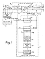
- FIG. 1 represents a block diagram of the first embodiment of the device according to the invention, which implements this method.
- three input terminals 1, 2 and 3 are shown, intended respectively to receive the three color signals V e1 , V e2 and V e3 supplied by the analyzer tubes of a color camera. These three input terminals are respectively coupled to the three inputs of a circuit 4 for determining a signal V e , constituted by a matrixing circuit 4. The output of this matrixing circuit 4 delivers the signal V e , which is consisting, in this example, of the global luminance signal.
- V e 0.11 ⁇ V e1 + 0.59 ⁇ V e2 + 0.3 ⁇ V e3 ⁇ (V e1 , V e2 and V e3 ) corresponding respectively to the blue, green and red color signals).
- the output of the matrixing circuit 4 is connected to an input of a control circuit 6.
- the control circuit 6 comprises means 14 for acquiring a histogram, an analog quadrupole 11 and an analog divider 10, each having a input connected to the circuit input command 6, and it further comprises calculation means 13 and auxiliary calculation means 12.
- the quadrupole 11 is non-linear and has variable characteristics adjustable by eight control inputs e 1 to e 8 intended to receive eight signals defining the quadrupole transfer parameters.
- This quadrupole 11 is of known type having a broken line transfer function consisting of a predetermined number of linear segments. In the example described, the quadrupole 11 was chosen with eight variable transfer parameters, that is to say four couples, consisting of a threshold value and a gain value, defining four segments.
- Such a quadrupole comprises four amplifiers (not shown), having an adjustable threshold below which no signal is transmitted and above which the signals are transmitted with a fixed gain.
- the quadrupole 11 delivers a corrected luminance signal F (V e ), F being the transfer function of the quadrupole.
- This signal F (V e ) corresponds to the sum of the four output signals of the four amplifiers of the quadrupole, it is supplied to a second input of the divider 10 and to a second output of the control circuit 6.
- the means 14 statistically analyze the amplitude distribution of 4,000 samples of the luminance signal V e , according to 64 given amplitude levels.
- the 4,000 samples result from the analysis of 4,000 domains covering an entire frame, and the 64 amplitude levels are distributed at regular intervals over the entire amplitude scale of the luminance.
- the means 14 therefore make it possible to acquire the representative function of the histogram of the luminance (number of samples for each of the 64 levels envisaged).
- the calculation means 13 calculate the integral of this function, this integral being, by definition, the cumulative distribution function of the amplitude levels of the samples.
- the auxiliary calculation means 12 having an input connected to the output of the means 13 and eight outputs respectively connected to the eight control inputs e 1 to e 8 of the quadrupole 11, calculate the values of the eight transfer parameters A 1 to A 4 and G 1 to G 4 to be applied to the control inputs e 1 to e e , A i to G i (i varying from 1 to 4) representing respectively the threshold values and the gain values quadrupole amplifiers.
- the calculated values are such that the transfer function F carried out by the quadrupole 11 is an approximation by segments of the cumulative distribution function calculated by the means 13.
- the parameter values thus determined remain fixed for the duration of the following frame.
- Such a transfer function transforms the luminance signal V e into a corrected signal F (V e ) for which the distribution of the values allows better vision whatever the shooting conditions.
- the distribution corresponds to an equalization of the histogram of the luminance associated with the signal F (V e ).
- the assembly constituted by the quadrupole 11, the means 14 for acquiring a histogram, the calculation means 13 and the auxiliary calculation means 12, corresponds exactly to the automatic control device described in detail in the patent application cited in beginning of this text.
- the aim of the invention is to correct the color information V e1 , V e2 and V e3 so that the overall luminance information, associated with the corrected color information, corresponds to the luminance information contained in the signal F (V e ) while retaining the original chromaticity of the analyzed image.
- the three input terminals 1, 2 and 3 are respectively connected to the first three inputs of a correction circuit 5 of which a second input, a third and a fourth inputs are connected respectively to the first output of the control circuit 6, at the output of the determination circuit 4, and at the second output of the control circuit 6.
- the correction circuit 5 is constituted, in this embodiment, by a subtraction circuit 7 having the first three inputs constituting the three first inputs of the correction circuit 5, by three analog multipliers 21, 22, 23 having three first inputs connected respectively to three outputs of the subtraction circuit 7, having three second inputs connected together to constitute the second input of the correction circuit 5, and having three outputs connected respectively to three inputs of an adder 9.
- the subtraction circuit 7 has a second input constituting the third input of the correction circuit.
- the adder 9 has a second input constituting the fourth input of the correction circuit 5 and three outputs constituting respectively three outputs of the correction circuit 5, which are connected to the three output terminals 15, 16, 17 of the device according to the invention.
- the subtraction circuit 7 has three outputs providing respectively three color difference signals DV e1 , DV e2 and DV e3 . These three signals are developed from the signals V el , V e2 , V e3 and V e according to the following formulas:
- the multipliers 21, 22, 23 respectively generate three signals DV s1 , DV s2 and DV s3 from the signals G (V e ), DV e1 , DV e2 and DV e3 according to the following formulas
- the three outputs of the adder 9 respectively supply three signals V s1 , V s2 and V s3 produced from the signals DV s1 , DV s2 , DV s3 and F (V e ) according to the following formulas:
- the correction circuit 5 transforms the color information V e1 , V e2 and V e3 associated with the global luminance signal V e into corrected color information V s1 , V s2 and V s3 associated with the corrected overall luminance signal F (V e ).
- V e the corrected overall luminance signal
- the quadrupole 11 may include any number of variable parameters in order to better adapt the transfer function to the cumulative distribution function; the same applies to the number of samples and the number of amplitude levels of the luminance signal.
- control device 6 or one of its elements can easily be produced using a microcomputer.
- V e It is also possible to directly generate the signal G (V e ) using a digital memory.
- the analog signal V e is then converted into digital values which are applied to the address inputs of a memory in which a microcomputer has previously stored the values of G (V e ).
- the output of the memory is then connected to the input of a digital-analog converter which delivers the signal G (V e ).
- the matrixing circuit 4 generates a signal V e which corresponds to the global luminance signal calculated with the conventional coefficients (0.11; 0.59; 0.3).
- the invention is applicable from a signal V e corresponding to a different combination of color information. For example, excellent results have been obtained by taking as signal V e the signal corresponding to max (V e1 ; V e2 ; V e3 ).
- the invention can easily be applied from the three color signals E Y , D R , D B , transmitted by color television. Indeed, the processing to be subjected to these three signals is deduced simply from that exposed for the three primary signals E B , E V and E R , these two triplets of signals being linked by linear relations.
- FIG. 2 represents a second embodiment of the device according to the invention.
- the determination circuit 4 supplies a signal with a value V e which is not equal to the overall luminance value, but which is equal to the largest of the values among those of the three signals of color, E R , E v , E B at the sampling instant considered:
- the correction consists in correcting the overall luminance while preserving the original chromaticity of the image when the value G (V e ) is high, but not when it is low.
- the corrected luminance value is greater than the original value, the device does not modify the saturation of the color.
- the corrected luminance value is lower than the original value, the perception of the image is improved by increasing the saturation of the color while maintaining the same hue.
- the signals of values V e1 , V e2 , V e3 consist of the global luminance signal of value Ey, and the color difference signals, of values D R and D B.
- the control circuit 6 develops the value G (V e ) by a digital process implemented by a microprocessor.
- a determination circuit 4 is constituted by a demosaicing circuit 25 having three inputs constituting three inputs of the determination circuit 4, and three outputs providing color signals of value E R , E V and E B , to three inputs of a selection circuit 26 which determines which of these values is the largest and routes this to an output constituting the output of the determination circuit 4.
- the value V e thus determined is applied to an input of the circuit of command 6.
- the control circuit 6 comprises an analog-digital converter 27 whose input constitutes the input of the control circuit 6 and which converts the value V e from the analog form to the digital form.
- the control circuit 6 comprises a digital-analog converter 28 whose output constitutes an output of the control circuit 6 and provides in analog form a signal with a value G (V e ).
- the control circuit 6 also comprises means 32 for acquiring a histogram, a digital integrator 31, a microprocessor 30, and a random access memory 29.
- the means 32 calculate for each frame of an image the histogram of 4 000 values V e supplied by the output of the analog-digital converter 27, and supply the values of this histogram to the digital integrator 31 which calculates the values of the function of the cumulative distribution of this histogram and supplies them to an input of the microprocessor 30.
- the microprocessor 30 has two outputs connected respectively to a write address input and to a data input from memory 29. It calculates a table of the values of the function G (V e ) and stores this table in the memory 29.
- a first stage consists in determining a function F such that the histogram of the values of the corrected signal F (V e ) has a predetermined distribution over the whole of its scale of val eurs. For example, to have a regular distribution it suffices that the function F (V Q ) is equal to the cumulative distribution function of the values V e .
- the microprocessor 30 calculates 64 values of G (V e ), each of these values being chosen from 256 possible values, coded on eight bits. These values are stored in memory 29 which comprises 256 bytes.
- This memory includes a read address input connected to the output of the analog-digital converter 27, and a data output connected to the input of the digital-analog converter 28.
- the output of the determination 4 provides a value V e which is transmitted in digital form to the reading address input of the memory 29, the latter provides on its data output a digital value G (V e ) which is converted into the form analog by the digital-analog converter 28, and which is applied to the output of the control circuit 6.
- the correction circuit 5 comprises three analog multipliers 21, 22 and 23 having three first inputs and three outputs, constituting respectively three first inputs and three outputs of the correction circuit 5, and having three second inputs.
- the second input of the multiplier 21 is connected to a second input of the correction circuit 5 and the second inputs of the multipliers 22 and 23 are connected together to the output of a weighting circuit 24 having an input connected to a second input of the correction 5.
- the weighting circuit 24 is an analog circuit supplying at its output a signal of value H (V e ) equal to 1 when G (V e ) is less than or equal to 1, and a signal of value H (V e ) equal to G (V e ) when G (V e ) is greater than 1.
- the value G (V e ) is transmitted without modification when it is high, so the chromaticity is preserved when the correction consists in increasing the luminance of a shade , and on the other hand the saturation of the color is increased when the luminance of a hue is decreased.
- weighting circuit 24 It is within the reach of those skilled in the art to produce a weighting circuit 24 operating differently, it is in particular possible to use a weighting circuit providing a value such as: H (V e ): 1/2 ⁇ G (V e ) + 1/2.
- V e Max (E R , E v , E B ) avoids an exaggerated correction of the luminance signal when one of the values of the color signals is much higher than the other two.
Description
La présente invention concerne les dispositifs de correction des informations couleur fournies par une caméra d'un système de transmission vidéo en vue d'obtenir en réception une image contenant le maximum d'informations visibles.The present invention relates to devices for correcting color information supplied by a camera of a video transmission system with a view to obtaining, on reception, an image containing the maximum of visible information.
Dans les systèmes de transmission d'images en noir et blanc, il est déjà connu un dispositif de correction en vue d'améliorer la perception des images (demande de brevet européen n° 19518 déposée par la Demanderesse). Le procédé mis en oeuvre par ce dispositif consiste à corriger le signal de luminance fourni par le tube analyseur d'une caméra noir et blanc à l'aide d'un quadripôle non linéaire à caractéristiques variables, commandé de telle façon que l'histogramme des valeurs du signal de luminance corrigé, a une forme plate quelles que soient les conditions de prises de vues, ce qui correspond à une répartition régulière des valeurs sur l'échelle de ces valeurs.In black and white image transmission systems, a correction device is already known in order to improve the perception of images (European patent application n ° 19518 filed by the Applicant). The method implemented by this device consists in correcting the luminance signal supplied by the analyzer tube of a black and white camera using a nonlinear quadrupole with variable characteristics, controlled in such a way that the histogram of the values of the corrected luminance signal, has a flat shape whatever the shooting conditions, which corresponds to a regular distribution of the values on the scale of these values.
Tel qu'il est conçu actuellement, ce dispositif de correction ne permet pas d'améliorer les images couleur. Il permet seulement d'améliorer les images en noir et blanc.As currently designed, this correction device does not make it possible to improve color images. It only improves the black and white images.
La présente invention a pour objet un dispositif de correction permettant d'améliorer la perception des images couleur. Le problème consiste à corriger la luminance globale selon la méthode mise en oeuvre par le dispositif connu tout en conservant la chromaticité originelle de l'image analysée.The present invention relates to a correction device for improving the perception of color images. The problem consists in correcting the overall luminance according to the method implemented by the known device while retaining the original chromaticity of the image analyzed.
Selon l'invention, un dispositif de correction des informations couleur, de valeurs Ve1, Ve2 et Ve3, fournies par une caméra de télévision, est caractérisé en ce qu'il comporte :
- - un circuit de détermination (4) ayant trois entrées recevant respectivement les trois informations couleur et une sortie, pour fournir un signal de valeur Ve, fonction des valeurs des informations couleur ;
- - un circuit de commande (6) ayant une entrée couplée à la sortie du circuit de détermination (4), et ayant une sortie, pour fournir un signal de valeur G(Ve) = F(Ve)Ne, où F est une fonction telle que l'histogramme des valeurs F(Ve) en fonction des valeurs Ve a une répartition prédéterminée, choisie pour améliorer la perception des images ;
- - un circuit de correction (5) ayant trois premières entrées recevant respectivement les trois informations couleur, une deuxième entrée couplée à la sortie du circuit de commande, et ayant trois sorties constituant les sorties du dispositif selon l'invention, pour fournir trois signaux fonctions de la veleur G(Ve) et des valeurs Ve1, Ve2, Ve3 respectivement.
- - a determination circuit (4) having three inputs receiving respectively the three color information and an output, for supplying a signal of value V e , function of the values of the color information;
- - a control circuit (6) having an input coupled to the output of the determination circuit (4), and having an output, for supplying a signal with a value G (V e ) = F (V e ) N e , where F is a function such that the histogram of the values F (V e ) as a function of the values V e has a predetermined distribution, chosen to improve the perception of the images;
- - a correction circuit (5) having three first inputs respectively receiving the three color information, a second input coupled to the output of the control circuit, and having three outputs constituting the outputs of the device according to the invention, to supply three function signals of the velocity G (V e ) and of the values V e1 , V e2 , V e3 respectively.
L'invention sera mieux comprise et d'autres caractéristiques apparaîtront à l'aide de la description ci-après et des figures s'y rapportant :
- la figure 1 représente un premier mode de réalisation du dispositif selon l'invention ;
- la figure 2 représente un deuxième mode de réalisation du dispositif selon l'invention.
- FIG. 1 represents a first embodiment of the device according to the invention;
- FIG. 2 represents a second embodiment of the device according to the invention.
Dans le premier mode de réalisation le dispositif selon l'invention reçoit les trois informations couleur, de valeur Ve1, Ve2, Ve3, constituées respectivement des trois signaux de couleur bleu, vert, rouge, de valeurs EB, Ev, ER, appliqués respectivement à trois bornes d'entrées 1, 2 et 3. Il fournit sur trois bornes de sorties, 15, 16, 17 trois informations de couleur corrigées, de valeurs : Vs1, Vs2, Vs3.In the first embodiment, the device according to the invention receives the three color pieces of information, of value V e1 , V e2 , V e3 , consisting respectively of the three signals of blue, green, red color, of values E B , E v , E R , applied respectively to three
La valeur de la luminance globale est :![]()
![]()
La correction de la luminance globale consiste à multiplier cette valeur par un coefficient variable G :![]()
![]()
La valeur Ey étant une combinaison linéaire de Ev, ER, EB, pour conserver la chromaticité il suffit de multiplier par le même coefficient G les trois valeurs EV, ER, EB. Le coefficient G varie quand Ey varie, car il est déterminé de façon à aplanir l'histogramme des valeurs Ve d'un signal qui est constitué, dans cet exemple de réalisation, par le signal de luminance globale. Le dispositif de correction selon l'invention fournit dans ce cas trois signaux de couleur ayant pour valeur corrigée :![]()
![]()
![]()
![]()
![]()
![]()
La figure 1 représente un schéma synoptique du premier mode de réalisation du dispositif selon l'invention, qui met en oeuvre ce procédé.FIG. 1 represents a block diagram of the first embodiment of the device according to the invention, which implements this method.
Sur cette figure, sont représentées trois bornes d'entrée 1, 2 et 3 destinées à recevoir respectivement les trois signaux couleur Ve1, Ve2 et Ve3 fournis par les tubes analyseurs d'une caméra couleur. Ces trois bornes d'entrée sont respectivement couplées aux trois entrées d'un circuit 4 de détermination d'un signal Ve, constitué par un circuit de matriçage 4. La sortie de ce circuit de matriçage 4 délivre le signal Ve, qui est constitué, dans cet exemple, du signal de luminance globale. Ce signal est déduit des informations couleur Ve1, Ve2 et Ve3 selon la formule suivante : Ve = 0,11 · Ve1 + 0,59 · Ve2 + 0,3 · Ve3 · (Ve1, Ve2 et Ve3) correspondant respectivement aux signaux de couleur bleu, vert et rouge).In this figure, three
La sortie du circuit de matriçage 4 est connectée à une entrée d'un circuit de commande 6. Le circuit de commande 6 comporte des moyens 14 d'acquisition d'un histogramme, un quadripôle analogique 11 et un diviseur analogique 10, ayant chacun une entrée reliée à l'entrée du circuit de commande 6, et il comporte en outre des moyens de calcul 13 et des moyens de calcul auxiliaires 12. Le quadripôle 11 est non linéaire et a des caractéristiques variables réglables par huit entrées de commande e1 à e8 destinées à recevoir huit signaux définissant les paramètres de transfert du quadripôle. Ce quadripôle 11 est de type connu ayant une fonction de transfert en ligne brisée constituée d'un nombre prédéterminé de segments linéaires. Dans l'exemple décrit, le quadripôle 11 a été choisi à huit paramètres de transfert variables, soit quatre couples, constitués d'une valeur de seuil et d'une valeur de gain, définissant quatre segments. Un tel quadripôle comporte quatre amplificateurs (non représentés), ayant un seuil réglable au-dessous duquel aucun signal n'est transmis et au-dessus duquel les signaux sont transmis avec un gain fixé. Ainsi, le quadripôle 11 délivre un signal de luminance corrigé F(Ve), F étant la fonction de transfert du quadripôle. Ce signal F(Ve) correspond à la somme des quatre signaux de sortie des quatre amplificateurs du quadripôle, il est fourni à une deuxième entrée du diviseur 10 et à une deuxième sortie du circuit de commande 6.The output of the matrixing circuit 4 is connected to an input of a
Les moyens 14 analysent statistiquement la répartition en amplitude de 4 000 échantillons du signal de luminance Ve, selon 64 niveaux d'amplitude donnés. Les 4 000 échantillons résultent de l'analyse de 4 000 domaines recouvrant toute une trame, et les 64 niveaux d'amplitude sont répartis suivant des intervalles réguliers sur toute l'échelle des amplitudes de la luminance. Les moyens 14 permettent donc d'acquérir la fonction représentative de l'histogramme de la luminance (nombre d'échantillons pour chacun des . 64 niveaux envisagés).The means 14 statistically analyze the amplitude distribution of 4,000 samples of the luminance signal V e , according to 64 given amplitude levels. The 4,000 samples result from the analysis of 4,000 domains covering an entire frame, and the 64 amplitude levels are distributed at regular intervals over the entire amplitude scale of the luminance. The
Les moyens de calcul 13, dont l'entrée est reliée à la sortie des moyens 14, calculent l'intégrale de cette fonction, cette intégrale étant, par définition, la fonction de répartition cumulative des niveaux d'amplitude des échantillons.The calculation means 13, the input of which is connected to the output of the
A partir de cette fonction de répartition cumulative, les moyens de calcul auxiliaires 12, ayant une entrée reliée à la sortie des moyens 13 et huit sorties respectivement reliées aux huit entrées de commande e1 à e8 du quadripôle 11, calculent les valeurs des huit paramètres de transfert A1 à A4 et G1 à G4 à appliquer aux entrées de commande e1 à ee, Ai à Gi (i variant de 1 à 4) représentant respectivement les valeurs de seuil et les valeurs de gain des amplificateurs du quadripôle. Les valeurs calculées sont telles que la fonction de transfert F réalisée par le quadripôle 11 est une approximation par segments de la fonction de répartition cumulative calculée par les moyens 13. Les valeurs de paramètres ainsi déterminées restent fixées pendant la durée de la trame suivante.From this cumulative distribution function, the auxiliary calculation means 12, having an input connected to the output of the
Une telle fonction de transfert transforme le signal de luminance Ve en un signal corrigé F(Ve) pour lequel la répartition des valeurs permet une meilleure vision quelles que soient les conditions de prise de vues. (Dans cet exemple la répartition correspond à une égalisation de l'histogramme de la luminance associée au signal F(Ve).)Such a transfer function transforms the luminance signal V e into a corrected signal F (V e ) for which the distribution of the values allows better vision whatever the shooting conditions. (In this example the distribution corresponds to an equalization of the histogram of the luminance associated with the signal F (V e ).)
L'ensemble constitué par le quadripôle 11, les moyens 14 d'acquisition d'un histogramme, les moyens de calcul 13 et les moyens de calcul auxiliaires 12, correspond exactement au dispositif de commande automatique décrit en détails dans la demande de brevet citée au début de ce texte. Le circuit de commande 6 comporte en plus le diviseur analogique 10 ayant deux entrées recevant respectivement des signaux de valeur Ve et F(Ve), et ayant une sortie, constituant la première sortie du circuit de commande, et fournissant un signal de valeur G(Ve) = F(Ve)Ne.The assembly constituted by the
Le but de l'invention est de corriger les informations couleurs Ve1, Ve2 et Ve3 afin que l'information de luminance globale, associée aux informations couleur corrigées, corresponde à l'information de luminance contenue dans le signal F(Ve) tout en conservant la chromaticité originelle de l'image analysée. Pour cela, les trois bornes d'entrée 1, 2 et 3 sont respectivement reliées aux trois premières entrées d'un circuit de correction 5 dont une deuxième entrée, une troisième et une quatrième entrées sont reliées respectivement à la première sortie du circuit de commande 6, à la sortie du circuit de détermination 4, et à la deuxième sortie du circuit de commande 6. Le circuit de correction 5 est constitué, dans cet exemple de réalisation, par un circuit de soustraction 7 ayant les trois premières entrées constituant les trois premières entrées du circuit de correction 5, par trois multiplicateurs analogiques 21, 22, 23 ayant trois premières entrées reliées respectivement à trois sorties du circuit de soustraction 7, ayant trois secondes entrées reliées ensemble pour constituer la deuxième entrée du circuit de correction 5, et ayant trois sorties reliées respectivement à trois entrées d'un additionneur 9. Le circuit de soustraction 7 possède une seconde entrée constituant la troisième entrée du circuit de correction. L'additionneur 9 possède une seconde entrée constituant la quatrième entrée du circuit de correction 5 et trois sorties constituant respectivement trois sorties du circuit de correction 5, qui sont reliées aux trois bornes de sortie 15, 16, 17 du dispositif selon l'invention. La deuxième et la quatrième entrée du circuit de correction 5 reçoivent respectivement une valeur G(Ve) = F(Ve)/Ve fournie par la sortie du diviseur 10 et la valeur F(Ve) fournie par la sortie du quadripôle 11. Le circuit de soustraction 7 comporte trois sorties fournissant respectivement trois signaux de différence de couleur DVe1, DVe2 et DVe3. Ces trois signaux sont élaborés à partir des signaux Vel, Ve2, Ve3 et Ve selon les formules suivantes :![]()
![]()
![]()
![]()
![]()
![]()
Les multiplicateurs 21, 22, 23 élaborent respectivement trois signaux DVs1, DVs2 et DVs3 à partir des signaux G(Ve), DVe1, DVe2 et DVe3 selon les formules suivantes![]()
![]()
![]()
![]()
![]()
![]()
Les trois sorties de l'additionneur 9 fournissent respectivement trois signaux Vs1, Vs2 et Vs3 élaborés à partir des signaux DVs1, DVs2, DVs3 et F(Ve) selon les formules suivantes :![]()
![]()
![]()
![]()
![]()
![]()
Selon le principe qui vient d'être explicité, le circuit de correction 5 transforme les informations couleur Ve1, Ve2 et Ve3 associées au signal de luminance globale Ve en des informations couleur corrigées Vs1, Vs2 et Vs3 associées au signal de luminance globale corrigé F(Ve). Ainsi, seule la luminance globale a été corrigée. La chromaticité originelle de l'image analysée n'est pas affectée par la correction apportée par le circuit de correction 5.According to the principle which has just been explained, the
L'invention n'est pas limitée au mode de réalisation décrit et représenté, de nombreuses variantes de réalisation sont possibles. En particulier, le quadripôle 11 peut comporter un nombre quelconque de paramètres variables afin de mieux adapter la fonction de transfert à la fonction de répartition cumulative ; il en est de même du nombre d'échantillons et du nombre de niveaux d'amplitude du signal de luminance.The invention is not limited to the embodiment described and shown, many variant embodiments are possible. In particular, the
Il a été pris comme exemple d'obtenir une égalisation de l'histogramme, mais toute autre répartition aurait pu être envisagée, ce qui aurait conduit à calculer une fonction de transfert différente de la fonction de répartition cumulative.It was taken as an example to obtain an equalization of the histogram, but any other distribution could have been envisaged, which would have led to calculate a transfer function different from the cumulative distribution function.
Il faut noter que le dispositif de commande 6 ou l'un de ses éléments peuvent facilement être réalisés à l'aide d'un micro-ordinateur.It should be noted that the
Il faut aussi noter que l'opération globale effectuée sur les signaux Ve1, Ve2 et Ve3 par le circuit de correction 5 consiste à multiplier chacun des trois signaux par le signal G(Ve). En effet, il est facile de vérifier que :![]()
![]()
![]()
![]()
![]()
![]()
Il est donc possible de réaliser le circuit de correction 5 d'une façon différente que celle précédemment décrite, en supprimant le circuit de soustraction 7 et l'additionneur 9. Le mode de réalisation décrit précédemment et représenté sur la figure 1 est plus complexe, mais il permet d'obtenir plus facilement la largeur de bande passante requise pour le signal de luminance.It is therefore possible to make the
Il est également possible de générer directement le signal G(Ve) à l'aide d'une mémoire numérique. Le signal analogique Ve est alors converti en valeurs numériques qui sont appliquées aux entrées d'adresse d'une mémoire dans laquelle un micro-ordinateur a préalablement stocké les valeurs de G(Ve). La sortie de la mémoire est ensuite reliée à l'entrée d'un convertisseur numérique-analogique qui délivre le signal G(Ve).It is also possible to directly generate the signal G (V e ) using a digital memory. The analog signal V e is then converted into digital values which are applied to the address inputs of a memory in which a microcomputer has previously stored the values of G (V e ). The output of the memory is then connected to the input of a digital-analog converter which delivers the signal G (V e ).
Dans le mode de réalisation décrit, le circuit de matriçage 4 élabore un signal Ve qui correspond au signal de luminance globale calculé avec les coefficients classiques (0,11 ; 0,59 ; 0,3). Mais l'invention est applicable à partir d'un signal Ve correspondant à une combinaison différente des informations couleurs. Par exemple, d'excellents résultats ont été obtenus en prenant comme signal Ve le signal correspondant à max (Ve1 ; Ve2; Ve3).In the embodiment described, the matrixing circuit 4 generates a signal V e which corresponds to the global luminance signal calculated with the conventional coefficients (0.11; 0.59; 0.3). However, the invention is applicable from a signal V e corresponding to a different combination of color information. For example, excellent results have been obtained by taking as signal V e the signal corresponding to max (V e1 ; V e2 ; V e3 ).
Enfin, il faut noter que l'invention peut facilement être appliquée à partir des trois signaux couleur EY, DR, DB, transmis en télévision couleur. En effet, le traitement à faire subir à ces trois signaux se déduit simplement de celui exposé pour les trois signaux primaires EB, EV et ER, ces deux triplets de signaux étant liés par des relations linéaires.Finally, it should be noted that the invention can easily be applied from the three color signals E Y , D R , D B , transmitted by color television. Indeed, the processing to be subjected to these three signals is deduced simply from that exposed for the three primary signals E B , E V and E R , these two triplets of signals being linked by linear relations.
La figure 2 représente un deuxième mode de réalisation du dispositif selon l'invention. D'une part, dans ce mode de réalisation le circuit de détermination 4 fournit un signal de valeur Ve qui n'est pas égale à la valeur de luminance globale, mais qui est égale à la plus grande des valeurs parmi celles des trois signaux de couleur, ER, Ev, EB à l'instant d'échantillonnage considéré :![]()
![]()
D'autre part, la correction consiste à corriger la luminance globale en conservant la chromaticité originelle de l'image lorsque la valeur G(Ve) est élevée, mais non lorsqu'elle est faible. Dans le premier cas, la valeur corrigée de la luminance est supérieure à la valeur d'origine, le dispositif ne modifie pas la saturation de la couleur. Dans ce deuxième cas la valeur corrigée de la luminance est inférieure à la valeur d'origine, la perception de l'image est améliorée en augmentant la saturation de la couleur tout en conservant la même teinte. Les signaux de valeurs Ve1, Ve2, Ve3, sont constitués par le signal de luminance globale de valeur Ey, et les signaux de différence de couleur, de valeurs DR et DB. Le circuit de commande 6 élabore la valeur G(Ve) par un procédé numérique mis en oeuvre par un microprocesseur.On the other hand, the correction consists in correcting the overall luminance while preserving the original chromaticity of the image when the value G (V e ) is high, but not when it is low. In the first case, the corrected luminance value is greater than the original value, the device does not modify the saturation of the color. In this second case the corrected luminance value is lower than the original value, the perception of the image is improved by increasing the saturation of the color while maintaining the same hue. The signals of values V e1 , V e2 , V e3 , consist of the global luminance signal of value Ey, and the color difference signals, of values D R and D B. The
Dans ce mode de réalisation un circuit de détermination 4 est constitué par un circuit de dématriçage 25 ayant trois entrées constituant trois entrées du circuit de détermination 4, et trois sorties fournissant des signaux de couleur de valeur ER, EV et EB, à trois entrées d'un circuit de sélection 26 qui détermine laquelle de ces valeurs est la plus grande et achemine celle-ci vers une sortie constituant la sortie du circuit de détermination 4. La valeur Ve ainsi déterminée est appliquée à une entrée du circuit de commande 6.In this embodiment a determination circuit 4 is constituted by a demosaicing circuit 25 having three inputs constituting three inputs of the determination circuit 4, and three outputs providing color signals of value E R , E V and E B , to three inputs of a
Le circuit de commande 6 comporte un convertisseur analogique-numérique 27 dont l'entrée constitue l'entrée du circuit de commande 6 et qui convertit la valeur Ve de la forme analogique à la forme numérique. Le circuit de commande 6 comporte un convertisseur numérique-analogique 28 dont la sortie constitue une sortie du circuit de commande 6 et fournit sous forme analogique un signal de valeur G(Ve). Le circuit de commande 6 comporte en outre des moyens 32 d'acquisition d'un histogramme, un intégrateur numérique 31, un microprocesseur 30, et une mémoire vive 29. Les moyens 32 calculent pour chaque trame d'une image l'histogramme de 4 000 valeurs Ve fournies par la sortie du convertisseur analogique-numérique 27, et fournissent les valeurs de cet histogramme à l'intégrateur numérique 31 qui calcule les valeurs de la fonction de la répartition cumulative de cet histogramme et les fournit à une entrée du microprocesseur 30. Le microprocesseur 30 possède deux sorties reliées respectivement à une entrée d'adresse d'écriture et à une entrée de données de la mémoire 29. Il calcule une table des valeurs de la fonction G(Ve) et stocke cette table dans la mémoire 29. Ce calcul est réalisé en deux étapes : une première étape consiste à déterminer une fonction F telle que l'histogramme des valeurs du signal corrigé F(Ve) a une répartition prédéterminée sur l'ensemble de son échelle de valeurs. Par exemple, pour avoir une répartition régulière il suffit que la fonction F(VQ) soit égale à la fonction de répartition cumulative des valeurs Ve. Dans une deuxième étape le microprocesseur 30 calcule les valeurs de la fonction G(Ve) = F(Ve)/Ve, en tenant compte d'une limitation de la valeur G(Ve) à 4, dans cet exemple, afin de ne jamais dénaturer l'image et de ne pas amplifier le bruit au point de le rendre visible. Dans cet exemple, le microprocesseur 30 calcule 64 valeurs de G(Ve), chacune de ces valeurs étant choisies parmi 256 valeurs possibles, codées sur huit bits. Ces valeurs sont stockées dans la mémoire 29 qui comporte 256 octets. Cette mémoire comporte une entrée d'adresse de lecture reliée à la sortie du convertisseur analogique-numérique 27, et une sortie de données reliée à l'entrée du convertisseur numérique-analogique 28. Pour chaque point d'une image la sortie du circuit de détermination 4 fournit une valeur Ve qui est transmise sous forme numérique à l'entrée d'adresse de lecture de la mémoire 29, celle-ci fournit sur sa sortie de données une valeur numérique G(Ve) qui est convertie sous la forme analogique par le convertisseur numérique-analogique 28, et qui est appliquée à la sortie du circuit de commande 6.The
Le circuit de correction 5 comporte trois multiplicateurs analogiques 21, 22 et 23 ayant trois premières entrées et trois sorties, constituant respectivement trois premières entrées et trois sorties du circuit de correction 5, et ayant trois secondes entrées. La seconde entrée du multiplicateur 21 est reliée à une seconde entrée du circuit de correction 5 et les secondes entrées des multiplicateurs 22 et 23 sont reliées ensemble à la sortie d'un circuit de pondération 24 ayant une entrée reliée à une deuxième entrée du circuit de correction 5.The
Le circuit de pondération 24 est un circuit analogique fournissant sur sa sortie un signal de valeur H(Ve) égale à 1 quand G(Ve) est inférieure ou égale à 1, et un signal de valeur H(Ve) égale à G(Ve) quand G(Ve) est supérieure à 1. La valeur G(Ve) est transmise sans modification lorsqu'elle est élevée, ainsi la chromaticité est conservée lorsque la correction consiste à augmenter la luminance d'une teinte, et par contre la saturation de la couleur est augmentée lorsque la luminance d'une teinte est diminuée.The
Il est à la portée de l'homme de l'art de réaliser un circuit de pondération 24 fonctionnant différemment, il est notamment possible d'utiliser un circuit de pondération fournissant une valeur telle que : H(Ve) : 1/2 · G(Ve) + 1/2.It is within the reach of those skilled in the art to produce a
Dans ce cas il y a une augmentation de la saturation de la couleur quand la luminance globale est diminuée, et diminution de la saturation de ces couleurs quand la luminance globale est augmentée.In this case there is an increase in the saturation of the color when the overall luminance is decreased, and a decrease in the saturation of these colors when the overall luminance is increased.
Il est aussi à la portée de l'homme de l'art de réaliser différemment le circuit de détermination 4 et de prendre pour valeur Ve une autre combinaison des signaux de couleurs. Prendre Ve = Max(ER, Ev, EB) permet d'éviter une correction exagérée du signal de luminance lorsque l'une des valeurs des signaux de couleur est très supérieure aux deux autres.It is also within the reach of those skilled in the art to carry out the determination circuit 4 differently and to take as value V e another combination of the color signals. Taking V e = Max (E R , E v , E B ) avoids an exaggerated correction of the luminance signal when one of the values of the color signals is much higher than the other two.
Claims (7)
Applications Claiming Priority (2)
| Application Number | Priority Date | Filing Date | Title |
|---|---|---|---|
| FR8110253 | 1981-05-22 | ||
| FR8110253A FR2506549A1 (en) | 1981-05-22 | 1981-05-22 | DEVICE FOR CORRECTING COLOR INFORMATION PROVIDED BY ANALYZER TUBES OF A CAMERA WITH A VIEW TO IMPROVING IMAGE PERCEPTION |
Publications (2)
| Publication Number | Publication Date |
|---|---|
| EP0067083A1 EP0067083A1 (en) | 1982-12-15 |
| EP0067083B1 true EP0067083B1 (en) | 1984-06-13 |
Family
ID=9258804
Family Applications (1)
| Application Number | Title | Priority Date | Filing Date |
|---|---|---|---|
| EP82400821A Expired EP0067083B1 (en) | 1981-05-22 | 1982-05-04 | Television camera colour correction circuit for improved image perception |
Country Status (6)
| Country | Link |
|---|---|
| US (1) | US4499486A (en) |
| EP (1) | EP0067083B1 (en) |
| JP (1) | JPS57197988A (en) |
| CA (1) | CA1197608A (en) |
| DE (1) | DE3260247D1 (en) |
| FR (1) | FR2506549A1 (en) |
Families Citing this family (20)
| Publication number | Priority date | Publication date | Assignee | Title |
|---|---|---|---|---|
| DE3480760D1 (en) * | 1983-09-16 | 1990-01-18 | Hitachi Ltd | SIGNAL PROCESSING CIRCUIT FOR A COLOR VIDEO CAMERA. |
| JPS60151786A (en) * | 1984-01-19 | 1985-08-09 | Fuji Photo Film Co Ltd | Processing method and device of radiation picture information reading gradation |
| FR2575884B1 (en) * | 1985-01-08 | 1988-07-08 | Thomson Video Equip | DEVICE FOR REDUCING THE DYNAMICS OF THREE COLOR SIGNALS REPRESENTING AN IMAGE |
| US4764971A (en) * | 1985-11-25 | 1988-08-16 | Eastman Kodak Company | Image processing method including image segmentation |
| JPH0669438B2 (en) * | 1987-04-24 | 1994-09-07 | 株式会社東芝 | Endoscope device |
| JPS6354144A (en) * | 1986-08-25 | 1988-03-08 | 株式会社東芝 | Electronic endoscope apparatus |
| DE3629396C2 (en) * | 1986-08-29 | 1993-12-23 | Agfa Gevaert Ag | Electronic image processing method |
| DE3629403C2 (en) * | 1986-08-29 | 1994-09-29 | Agfa Gevaert Ag | Method of correcting color saturation in electronic image processing |
| JP2522296B2 (en) * | 1987-03-31 | 1996-08-07 | ソニー株式会社 | Video signal gradation control circuit |
| US4868651A (en) * | 1988-05-17 | 1989-09-19 | S&S Inficon, Inc. | Digital radiography with image brightness and contrast normalization |
| JP2582140B2 (en) * | 1988-10-31 | 1997-02-19 | 株式会社日立製作所 | Projection display |
| CA2040672C (en) * | 1990-04-26 | 1995-05-30 | Masaaki Kanashiki | Image signal processing apparatus |
| US5137364A (en) * | 1991-01-31 | 1992-08-11 | Mccarthy Cornelius J | Optical spectral analysis apparatus |
| BE1007590A3 (en) * | 1993-10-01 | 1995-08-16 | Philips Electronics Nv | Video signal processing circuit. |
| JP3134660B2 (en) * | 1994-04-14 | 2001-02-13 | 松下電器産業株式会社 | Color conversion method and color conversion device |
| JP3408316B2 (en) * | 1994-04-18 | 2003-05-19 | 日本フィリップス株式会社 | Knee circuit |
| US6215529B1 (en) * | 1997-03-06 | 2001-04-10 | Matsushita Electric Industrial Co. Ltd. | Gamma compensation apparatus |
| JP4257036B2 (en) * | 1999-02-05 | 2009-04-22 | コーニンクレッカ フィリップス エレクトロニクス エヌ ヴィ | Histogram equalization method |
| EP1404116A1 (en) * | 2002-09-25 | 2004-03-31 | Dialog Semiconductor GmbH | Method for fast color saturation control |
| JP2008242733A (en) * | 2007-03-27 | 2008-10-09 | Seiko Epson Corp | Image processing apparatus |
Family Cites Families (9)
| Publication number | Priority date | Publication date | Assignee | Title |
|---|---|---|---|---|
| DE2018149C3 (en) * | 1970-04-16 | 1975-08-28 | Robert Bosch Gmbh, 7000 Stuttgart | Process for increasing the sharpness of color television pictures and circuit arrangement for carrying out the process |
| US3684825A (en) * | 1971-02-19 | 1972-08-15 | Rca Corp | Contrast compression circuits |
| US3979555A (en) * | 1975-05-27 | 1976-09-07 | Hughes Aircraft Company | Histogram equalization system for display improvement |
| US3983320A (en) * | 1975-08-25 | 1976-09-28 | Hughes Aircraft Company | Raster display histogram equalization |
| GB2046051B (en) * | 1979-03-29 | 1983-01-26 | Philips Electronic Associated | Real time histogram modification system for image processing |
| FR2456448A1 (en) * | 1979-05-11 | 1980-12-05 | Thomson Csf | DEVICE FOR AUTOMATICALLY CONTROLLING THE TRANSFER FUNCTION OF A VIDEO FREQUENCY TRANSMISSION SYSTEM WITH A VIEW TO IMPROVING IMAGE PERCEPTION |
| IL58119A (en) * | 1979-08-27 | 1983-03-31 | Yeda Res & Dev | Histogram image enhancement system |
| US4315319A (en) * | 1980-02-01 | 1982-02-09 | Rockwell International Corporation | Non-linear signal processor |
| US4394744A (en) * | 1981-02-12 | 1983-07-19 | The United States Of America As Represented By The Secretary Of The Navy | Real-time amplitude histogram shaper |
-
1981
- 1981-05-22 FR FR8110253A patent/FR2506549A1/en active Granted
-
1982
- 1982-05-04 EP EP82400821A patent/EP0067083B1/en not_active Expired
- 1982-05-04 DE DE8282400821T patent/DE3260247D1/en not_active Expired
- 1982-05-18 CA CA000403228A patent/CA1197608A/en not_active Expired
- 1982-05-19 US US06/379,945 patent/US4499486A/en not_active Expired - Fee Related
- 1982-05-21 JP JP57087176A patent/JPS57197988A/en active Pending
Also Published As
| Publication number | Publication date |
|---|---|
| FR2506549A1 (en) | 1982-11-26 |
| JPS57197988A (en) | 1982-12-04 |
| US4499486A (en) | 1985-02-12 |
| EP0067083A1 (en) | 1982-12-15 |
| DE3260247D1 (en) | 1984-07-19 |
| CA1197608A (en) | 1985-12-03 |
| FR2506549B1 (en) | 1983-10-07 |
Similar Documents
| Publication | Publication Date | Title |
|---|---|---|
| EP0067083B1 (en) | Television camera colour correction circuit for improved image perception | |
| Mann et al. | Beingundigital’with digital cameras | |
| US9386288B2 (en) | Compensating for sensor saturation and microlens modulation during light-field image processing | |
| CA2013750C (en) | Method for adaptively sharpening electronic images | |
| EP0192497B1 (en) | Apparatus to compress the dynamic range of the three colour signals constituting a picture | |
| EP0298978B1 (en) | Digital color image processing method employing histogram normalization for tone and color reproduction | |
| US5319472A (en) | Multispectral color image pickup system | |
| CA1229911A (en) | Apparatus and method for producing a still image video signal using solid-state imaging device | |
| EP0019518B1 (en) | Device for automatically controlling the transfer function of a video frequency transmission system in order to improve picture perception | |
| EP0419342A1 (en) | Device for correcting errors of an image sequence analysed by an integrated matrix infrared sensor | |
| EP1286553B1 (en) | Method and apparatus for improving image quality in digital cameras | |
| WO1984002822A1 (en) | Continuous color correction process applicable to video shooting and system implementing that process | |
| EP3973693A1 (en) | Multi-exposure image capturing device and associated system for monitoring a driver | |
| EP0252566B1 (en) | Scintillation camera | |
| FR2577735A1 (en) | VIDEO SIGNAL ACCENTATION CIRCUIT | |
| CA1226654A (en) | Radar echos discriminating device | |
| EP0609117A1 (en) | Gain compensated gamma camera | |
| FR2563069A1 (en) | PARCELLAR LINEAR PROCESSING DEVICE FOR DIGITAL VIDEO SIGNALS | |
| EP0085600A1 (en) | Device for the correction of intermodulation produced by an amplifier for high-frequency signals with peak value regulation | |
| FR2736741A1 (en) | METHOD FOR PROCESSING A SOURCE SEQUENCE OF BLINKING DIGITAL IMAGES | |
| EP0240395A1 (en) | Method and device for the gamma-correction of a multi-colour cathode ray tube | |
| EP0061377A1 (en) | Digital signal demodulator and a colour television receiver or system comprising such a demodulator | |
| KR100727837B1 (en) | An image signal processing device of the camera system | |
| EP0024973B1 (en) | Keying signal generator for television inlay effect and special effects control device comprising such a generator | |
| EP0370152B1 (en) | Method and device for digital data transmission |
Legal Events
| Date | Code | Title | Description |
|---|---|---|---|
| PUAI | Public reference made under article 153(3) epc to a published international application that has entered the european phase |
Free format text: ORIGINAL CODE: 0009012 |
|
| AK | Designated contracting states |
Designated state(s): BE DE FR GB NL |
|
| 17P | Request for examination filed |
Effective date: 19830510 |
|
| GRAA | (expected) grant |
Free format text: ORIGINAL CODE: 0009210 |
|
| AK | Designated contracting states |
Designated state(s): BE DE FR GB NL |
|
| REF | Corresponds to: |
Ref document number: 3260247 Country of ref document: DE Date of ref document: 19840719 |
|
| PLBE | No opposition filed within time limit |
Free format text: ORIGINAL CODE: 0009261 |
|
| STAA | Information on the status of an ep patent application or granted ep patent |
Free format text: STATUS: NO OPPOSITION FILED WITHIN TIME LIMIT |
|
| 26N | No opposition filed | ||
| PGFP | Annual fee paid to national office [announced via postgrant information from national office to epo] |
Ref country code: NL Payment date: 19860531 Year of fee payment: 5 |
|
| PG25 | Lapsed in a contracting state [announced via postgrant information from national office to epo] |
Ref country code: NL Effective date: 19871201 |
|
| NLV4 | Nl: lapsed or anulled due to non-payment of the annual fee | ||
| BERE | Be: lapsed |
Owner name: THOMSON-CSF Effective date: 19880531 |
|
| PGFP | Annual fee paid to national office [announced via postgrant information from national office to epo] |
Ref country code: DE Payment date: 19890424 Year of fee payment: 8 |
|
| PGFP | Annual fee paid to national office [announced via postgrant information from national office to epo] |
Ref country code: GB Payment date: 19890430 Year of fee payment: 8 |
|
| PGFP | Annual fee paid to national office [announced via postgrant information from national office to epo] |
Ref country code: FR Payment date: 19890523 Year of fee payment: 8 |
|
| PG25 | Lapsed in a contracting state [announced via postgrant information from national office to epo] |
Ref country code: BE Effective date: 19890531 |
|
| PG25 | Lapsed in a contracting state [announced via postgrant information from national office to epo] |
Ref country code: GB Effective date: 19900504 |
|
| GBPC | Gb: european patent ceased through non-payment of renewal fee | ||
| PG25 | Lapsed in a contracting state [announced via postgrant information from national office to epo] |
Ref country code: FR Effective date: 19910131 |
|
| REG | Reference to a national code |
Ref country code: FR Ref legal event code: ST |
|
| PG25 | Lapsed in a contracting state [announced via postgrant information from national office to epo] |
Ref country code: DE Effective date: 19911001 |