EP0064890A1 - Device for picture-scanning in successive lines using electrical-charge transfer, comprising a line memory, and television camera comprising such a device - Google Patents
Device for picture-scanning in successive lines using electrical-charge transfer, comprising a line memory, and television camera comprising such a device Download PDFInfo
- Publication number
- EP0064890A1 EP0064890A1 EP82400632A EP82400632A EP0064890A1 EP 0064890 A1 EP0064890 A1 EP 0064890A1 EP 82400632 A EP82400632 A EP 82400632A EP 82400632 A EP82400632 A EP 82400632A EP 0064890 A1 EP0064890 A1 EP 0064890A1
- Authority
- EP
- European Patent Office
- Prior art keywords
- charges
- grid
- charge
- potential
- diodes
- Prior art date
- Legal status (The legal status is an assumption and is not a legal conclusion. Google has not performed a legal analysis and makes no representation as to the accuracy of the status listed.)
- Granted
Links
- 230000003071 parasitic effect Effects 0.000 claims abstract description 22
- 239000011159 matrix material Substances 0.000 claims abstract description 18
- 238000002347 injection Methods 0.000 claims abstract description 11
- 239000007924 injection Substances 0.000 claims abstract description 11
- 238000010191 image analysis Methods 0.000 claims abstract description 8
- 239000000758 substrate Substances 0.000 claims description 20
- 230000000737 periodic effect Effects 0.000 claims description 19
- 230000004888 barrier function Effects 0.000 claims description 18
- 238000002955 isolation Methods 0.000 claims description 18
- 239000004065 semiconductor Substances 0.000 claims description 15
- 230000006870 function Effects 0.000 claims description 12
- 238000005286 illumination Methods 0.000 claims description 5
- 238000009413 insulation Methods 0.000 claims description 4
- 238000011144 upstream manufacturing Methods 0.000 claims description 4
- 230000005855 radiation Effects 0.000 claims description 2
- 238000010586 diagram Methods 0.000 description 48
- 230000000694 effects Effects 0.000 description 5
- 244000045947 parasite Species 0.000 description 4
- 238000005036 potential barrier Methods 0.000 description 4
- 238000004458 analytical method Methods 0.000 description 3
- 230000008030 elimination Effects 0.000 description 3
- 238000003379 elimination reaction Methods 0.000 description 3
- 230000010354 integration Effects 0.000 description 3
- 230000000717 retained effect Effects 0.000 description 3
- 230000008859 change Effects 0.000 description 2
- 230000000295 complement effect Effects 0.000 description 2
- 230000008878 coupling Effects 0.000 description 2
- 238000010168 coupling process Methods 0.000 description 2
- 238000005859 coupling reaction Methods 0.000 description 2
- 238000007599 discharging Methods 0.000 description 2
- 238000009432 framing Methods 0.000 description 2
- 230000009545 invasion Effects 0.000 description 2
- 238000004519 manufacturing process Methods 0.000 description 2
- 230000008520 organization Effects 0.000 description 2
- 230000035515 penetration Effects 0.000 description 2
- 230000009467 reduction Effects 0.000 description 2
- 239000000243 solution Substances 0.000 description 2
- 240000008042 Zea mays Species 0.000 description 1
- 229910052782 aluminium Inorganic materials 0.000 description 1
- XAGFODPZIPBFFR-UHFFFAOYSA-N aluminium Chemical compound [Al] XAGFODPZIPBFFR-UHFFFAOYSA-N 0.000 description 1
- 230000008901 benefit Effects 0.000 description 1
- 230000000903 blocking effect Effects 0.000 description 1
- 238000004891 communication Methods 0.000 description 1
- 238000001514 detection method Methods 0.000 description 1
- 229910052751 metal Inorganic materials 0.000 description 1
- 239000002184 metal Substances 0.000 description 1
- 230000003287 optical effect Effects 0.000 description 1
- 229910021420 polycrystalline silicon Inorganic materials 0.000 description 1
- 230000035945 sensitivity Effects 0.000 description 1
- 238000000926 separation method Methods 0.000 description 1
- 239000007787 solid Substances 0.000 description 1
Images


Classifications
-
- H—ELECTRICITY
- H01—ELECTRIC ELEMENTS
- H01L—SEMICONDUCTOR DEVICES NOT COVERED BY CLASS H10
- H01L27/00—Devices consisting of a plurality of semiconductor or other solid-state components formed in or on a common substrate
- H01L27/14—Devices consisting of a plurality of semiconductor or other solid-state components formed in or on a common substrate including semiconductor components sensitive to infrared radiation, light, electromagnetic radiation of shorter wavelength or corpuscular radiation and specially adapted either for the conversion of the energy of such radiation into electrical energy or for the control of electrical energy by such radiation
- H01L27/144—Devices controlled by radiation
- H01L27/146—Imager structures
- H01L27/14643—Photodiode arrays; MOS imagers
-
- H—ELECTRICITY
- H04—ELECTRIC COMMUNICATION TECHNIQUE
- H04N—PICTORIAL COMMUNICATION, e.g. TELEVISION
- H04N25/00—Circuitry of solid-state image sensors [SSIS]; Control thereof
- H04N25/60—Noise processing, e.g. detecting, correcting, reducing or removing noise
- H04N25/62—Detection or reduction of noise due to excess charges produced by the exposure, e.g. smear, blooming, ghost image, crosstalk or leakage between pixels
- H04N25/626—Reduction of noise due to residual charges remaining after image readout, e.g. to remove ghost images or afterimages
-
- H—ELECTRICITY
- H04—ELECTRIC COMMUNICATION TECHNIQUE
- H04N—PICTORIAL COMMUNICATION, e.g. TELEVISION
- H04N25/00—Circuitry of solid-state image sensors [SSIS]; Control thereof
- H04N25/70—SSIS architectures; Circuits associated therewith
- H04N25/71—Charge-coupled device [CCD] sensors; Charge-transfer registers specially adapted for CCD sensors
- H04N25/713—Transfer or readout registers; Split readout registers or multiple readout registers
-
- H—ELECTRICITY
- H04—ELECTRIC COMMUNICATION TECHNIQUE
- H04N—PICTORIAL COMMUNICATION, e.g. TELEVISION
- H04N3/00—Scanning details of television systems; Combination thereof with generation of supply voltages
- H04N3/10—Scanning details of television systems; Combination thereof with generation of supply voltages by means not exclusively optical-mechanical
- H04N3/14—Scanning details of television systems; Combination thereof with generation of supply voltages by means not exclusively optical-mechanical by means of electrically scanned solid-state devices
- H04N3/15—Scanning details of television systems; Combination thereof with generation of supply voltages by means not exclusively optical-mechanical by means of electrically scanned solid-state devices for picture signal generation
- H04N3/155—Control of the image-sensor operation, e.g. image processing within the image-sensor
- H04N3/1568—Control of the image-sensor operation, e.g. image processing within the image-sensor for disturbance correction or prevention within the image-sensor, e.g. biasing, blooming, smearing
Definitions
- the present invention relates to the field of electrical analysis of light images in successive lines, constituting frames, using a charge transfer device comprising a line memory.
- Various solid state devices are known for analyzing a light image, which are intended to be used in a television camera to provide an electrical video signal. They are distinguished by the embodiment of the photosensitive area on the one hand, and the system for reading and discharging the charges created by the image, on the other hand.
- the present invention relates to an image analysis device of the line transfer type described above, in which the assembly has been perfected ensuring the storage of successive lines and the evacuation of parasitic charges, in order to improve the processing of small signals and reduce noise.
- the invention also relates to a television camera comprising such an image analysis device.
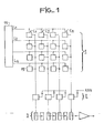
- FIG. 1 therefore represents the general organization of a line transfer structure, as described in the aforementioned French patent application.
- This structure mainly comprises a photosensitive area 1, a line memory 2 and an analog output shift register 3.
- the photosensitive zone 1 receives the light image to be analyzed and transforms it into electrical charges, called signal charges. It should be noted that the aim here is by luminepse image, the detection not only of the visible wavelengths but also of those which surround them, in particular in the infrared.
- the photosensitive zone is constituted by a plurality of elementary zones 15, also called below dots, arranged in N rows, marked L 1 , L 2 ... L N and M columns, marked C 1 , C 2 ... C M , and forming a matrix.
- the photosensitive points of the same line are linked together and connected to a control device 14, making it possible to address the lines one after the other; this device is constituted for example by a shift register. of the MOS type.
- the photosensitive points 15 of the same column are connected to the same connection, hereinafter called column connection, to the line memory 2.
- the line memory 2 therefore receives in parallel the signal charges created in each of the photosensitive points 15 of the same line, then it also transfers them in parallel to the register 3.
- a device for leveling (RAN connection in the figure) the column connections and a device for eliminating parasitic charges (not shown in figure 1).
- Register 3 is an analog shift register which provides information, received in parallel, in serial mode. This information constitutes the video signal for analyzing the optical image received on the photosensitive zone 1.
- the register is preferably charge transfer, of CCD type.
- the content of the line memory 2 is transferred to the shift register 3, the entry of the line memory then being closed.
- the next step corresponds to the line feed time during which the content of the line memory 2 is poured into the register 3, the latter having been completely read during the previous step.
- the selection of a line, its transfer to the line memory and then to the shift register is carried out entirely during the line return time, the time line being reserved for the updating of the reading means, which is all the better the longer it is, and for the serial evacuation of the shift register.
- FIG. 2 represents a top view of a first embodiment of the device according to the invention.
- connections have been shown coming from the M columns C of the photosensitive matrix (C i-1 , C i , C i + 1 in the figure) each ending in a diode D 2 , called charge reception diode signal (Q si ) from the matrix; it is produced for example by doping a semiconductor substrate which is advantageously the same as that on which the photosensitive matrix is produced 1.
- the device therefore comprises M charge transfer columns, delimited by isolation barriers 42, corresponding respectively to the M column connections of the photosensitive matrix.
- the diodes D 2 are aligned and are below adjacent to an electrode, or grid, G 1 in the form of a strip, which has the function of constituting a screen for the charges between the diodes D 2 and the rest of the device represented in FIG. 2 , which avoids the sending of parasitic charges on the column C connections: in fact, in charge transfer devices, it is particularly important to protect against parasitic charges, the amplitude of which can vary from a point to the other of the circuit according to the geometrical variations of the elements and which limit the dynamics of the signal.
- the gate G 1 is connected to a constant potential V 1 .
- a grid G 4 whose function is to store the charges, which is in the form of a strip having notches 24, for example rectangular, between two columns and one column out of two.
- a diode D 5 In at least a part of each of these notches 24 is made a diode D 5 , having for function the eva- cuation of parasitic charges; the diodes D 5 are connected to a potential V D5 periodic.
- the grid G 2 is surrounded by two coplanar grids G 1 and G 4 .
- the width of the grid G 2 is determined in a single photoengraving operation by the interval between the grids G l and G4. A better homogeneity is therefore obtained over the width of the grid G 2 which can be made much smaller.
- this embodiment has the advantage of increasing the speed of the transfer of the signal charges from D 1 and D 2 into memory, because of the reduction in the width of G 2 .
- the device also comprises a grid G 5 in the form of a strip, covering the storage grid G 4 , by means of an insulating layer, at the level of the notches 24, so as to be adjacent to the diodes D5; the gate G 5 receives a periodic potential V 5 and makes it possible to control the access of the charges to the diodes D 5 .
- the isolation barriers 42 are interrupted at the notches 24 or end, in the case where there is no notch, by an enlargement, for example in the shape of a triangle 43.
- the diodes D5 are surrounded by an isolation barrier 44 in the shape of a U, so that the diode D 5 remains accessible to the loads coming from the diodes D 2 of each of the columns.
- two channels are defined per column: one first channel, noted CL 1 , limited by an isolation barrier 42, its widening 43, and a branch of the U 44 on the outer side, and a second channel, noted CL 2 , limited by the inner side of the same U 44 and the second isolation barrier 42 limiting the column under consideration.
- Register 3 is a two-phase CCD register ⁇ 1 and ⁇ 2 . It consists of two sets of storage electrodes (31, 32) and two sets of transfer electrodes (33, 34), all of substantially rectangular shape, and placed perpendicular to the grids G 1 to G 7 above .
- the grids 31 are connected to the periodic potential ⁇ 1 and the grids 32, to the periodic potential ⁇ 2 ; the grids 33 and 34 are placed respectively between the pairs of grids 32-31 and 31-32, in the direction of charge transfer, on an extra thickness of insulation and are connected respectively to the potentials ⁇ 1 and ⁇ 2 .
- the electrodes of the register 3 are placed so that the electrodes 31 originate on the isolation barriers 43 or 44, the electrodes 32 being in the extension of the channels CL 1 .
- the damper 3 is bounded below by a horizontal isolation barrier 44, as the device is bounded above by a also horizontal isolation barrier 41.
- the various isolation barriers described above or below can be produced in any known way, such as an overdoping of the substrate, of the same type of conductivity as that last, or a localized excess thickness of the insulating layer (in general oxide) covering the substrate, the latter solution being able to be accompanied by an overdoping of the substrate produced under the insulation excess thickness.
- the various electrodes can also be produced in any known way: metal or polycrystalline silicon for example.
- each diode and part of the neighboring grids is covered with a layer opaque to light rays, such as a layer of aluminum.
- Figure 3a shows a sectional view of the device of the FIG. 2, and diagrams 3b to 3h, the illustration of the surface potential in the semiconductor substrate at different times, the surface potential being represented on these diagrams as on the following ones increasing downwards.
- a photosensitive point of the matrix has been represented.
- it is constituted by a grid G L constituting an electrode of a photodetector MOS capacity, brought to a periodic potential V GL , slightly covering the grid which follows it, marked G E , which is a screen for the charges, separating the photosensitive zone proper from the column connection, and which is brought to a constant potential V GE ; the screen grid G E is followed by a reading diode D L , produced in the substrate, starting point of the column connection c i .
- the photosensitive point comprises a second zone for detecting the light image, the frequency sensitivity of which is complementary to the MOS capacity, produced for example by a photodiode.
- an operation in volume transfer is shown by way of example, and therefore a doped (hatched) area denoted TV extending under the electrodes of register 3 up to half of the grid G 7 .
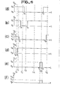
- FIG. 4 shows in its various diagrams (a to e) the evolution over time of the control signals applied to the device of FIG. 3.
- Diagram 4a represents the potential V GL which is at a constant high level (V H ), except during a time interval T 4 to T 7 , which corresponds to the transfer time of the charges accumulated in the photosensitive point considered towards the memory line then register 3 of Figure 2, and which corresponds substantially to the line return time.
- Diagram 4b represents the potential V 4 which is at a constant high level (V H ), except between instants T 3 and T5 framing the instant T 4 above .
- Diagram 4c represents the potential V 5 which is at a high level (V H ) until an instant T o at which it passes to a level intermediate (V I ) where it remains until an instant T 2 , T 0 and T 2 being prior to the previous instant T 3 . From the instant T 2 , V5 remains at a low level (V B ) until an instant T 8 , posterior to the instant T 7 , to which it rises to the high level V H.
- Diagram 4d represents the potential V D5 which is at a constant high level (V H ) except between the instant T 0 and an instant T 1 between T 0 and T 2 , duration during which it is at a low level (V B ).
- Diagram 4e represents the potential V 7 which is at a constant low level, except between an instant T 6 , prior to the instant T 7 , and T 7 , duration during which it is at a high level (V H ).
- the diode D 5 is at the low level, which allows the injection of charges under the gate G 4 , this injection being limited by the constant potential V 2 applied to the grid G 2 , which implies that the low level of V D5 is greater than the potential V 2 . It thus appears that the grid G 2 fixes the level of the potential of the column connections c i . Furthermore, to the left of line XX, a quantity of signal charge Q si is present under the grid G L (hatched area).
- FIG. 3c represents the potentials at an instant t 1 between T 1 and T 2 .
- the potential V D5 is at the high level and, therefore, a quantity of charge Q 0 is isolated under the grid G 4 (hatched area) by the potentials V 2 and V 5 applied respectively to the grids G 2 and G 5 .
- This quantity of charge Q 0 depends on the potential V I which is then applied under the gate G 5 , the potential V 2 being assumed to be lower than V I.
- the poten tiel applied to the grid G L of the MOS capacity of the photosensitive zone is brought to the low level, which has the effect of transferring the amount of charge Q if to the diodes D L (arrow 52 on the left part of FIG. 3d ).
- the diagram 3e represents the situation at an instant t4, between the instants T 5 and T 6 .
- the potential applied to the grid G4 is brought to the high level, which allows the transfer (arrow 53) of the charges Q 0 + Q if under the grid G 4 , and this in the two channels, which is shown to the right and left of the YY axis.
- Diagram 3f represents the situation at an instant t 5 situated between T6 and T 7 , period during which the potentials of channel CL 2 are unchanged, but the grid G 7 placed on channel CL 1 sees its potential increasing, which allows the transfer (arrow 54) of the charges Q 0 + Q if present under the gate G 4 towards the shift register 3, materialized by one of its electrodes 32. It thus appears that the quantity of known charge Q O is effectively transferred into the register 3, at the same time as the signal load Q if .
- this charge Q 0 in the register 3 is avoided, while only transferring the signal charge Q if , which makes it possible to eliminate the so-called spatial noise on Q 0 from one column to the other, noise due to variations in charges introduced by variations in the thickness of the oxide covering the substrate, a variation in threshold voltages, etc.
- This can be achieved by bringing the gate G 7 to an intermediate potential V I , shown in diagram 4f, the amplitude of which is between V B and V HI during the instants T 6 to T 7 , the value V I of this intermediate potential advantageously being equal to the intermediate potential applied to the gate G 5 between the instants T 0 and T 2 .
- the residual spatial noise can only be due to variations in threshold, doping or thickness of insulation between the gates G 7 and G 5 , which is very minimal in practice, taking into account the geometric proximity of these two grids.
- This structure therefore makes it possible to inject a predetermined quantity Q 0 of charges first under the storage grid G 4 , then on the diodes D L and D 2 establishing the connection between the photosensitive matrix and the line memory, in order to improve signal transfer charge Q if .
- This quantity of charges Q 0 is thus injected using the structure of the line memory and of the device for eliminating parasitic charges, and therefore without requiring an auxiliary device.
- each diode for discharging parasitic charges (D 5 ) is common to two columns, this. which makes it possible either to increase the storage capacity of the line memory (more extensive grid G 4 ), or to allow a smaller horizontal pitch and therefore a smaller footprint of the device.
- FIG. 5 represents a top view of a second embodiment of the invention where the generation of the quantity of charge Q O is completely free of spatial noise.
- each of the columns is divided vertically by an isolation barrier 45, delimiting on its left a first channel marked CL 1 , going from the grid G 4 to an electrode 32, on its right a second channel marked CL 2 and containing the diode D5, which then extends between the barriers 45 and 42, and finally a third channel, marked CL 3 , going from the electrode 31 of the register 3 towards the diode D5, that is to say opposite the channel CL 2 .
- La.figure 6a represents, on the left of an axis ZZ, a section along a closed line CC, produced from the diode D5 around the isolation barrier 45 of FIG. 5, and to the right of the axis ZZ , a section made along a line DD from the grid G 4 to the diode D 2 , these two sections being combined on the same diagram for the clarity of the explanation of the operation of the device of FIG. 5.
- a doping zone has been shown extending from the gate G 7 to the electrodes 31, 32 and 33 of the register 3, corresponding to the volume transfer type operation of this register.
- FIG. 7 represents in its different diagrams (a to f), the evolution over time of the different control signals applied to the device of FIG. 5, these control signals being periodic potentials whose amplitude varies between a low level , denoted VB for all the diagrams, and a high level, denoted V H also for all the diagrams, for simplicity, these different potentials are not necessarily equal.
- Diagram 7a represents the potential V 5 which is at a high level, except from an instant T 2 until an instant T 8 , the duration T 2 .T 8 being substantially that of line return.
- Diagram 7b represents the potential V D5 which is at a high level, except between two instants T 1 and T 3 , framing the instant T 2 above , where it is at a low level.
- Diagram 7c represents the potential V 7 which is at a low level until an instant T 4 posterior to the instant T3 at which it passes to a high level, until an instant T 5 posterior, where it returns to the low level , until a later time T 6 , where it returns to the high level until T 8 , where it returns to the low level.
- Diagram 7d represents the potential ⁇ 2 which is a signal in time slots of period T up to an instant T o prior to the instant T 1 at which it goes high until the instant T 5 at which it goes to a low level which it maintains until time T 6 at which it passes to a high level until time T 8 where it becomes again a signal in time slots of the same period as previously.
- the diagram 7e represents the potential ⁇ 1 which is complementary to the signal ⁇ 2 .
- Diagram 7f represents the potential V 4 which is at a high level until the instant T 5 where it passes to a low level until an instant T 7 between T 6 and T 8 , instant at which it returns to the level high.
- FIG. 6b represents the surface potential in the semiconductor at the level of FIG. 6a, at an instant t o comprised between T 1 and T 2 .
- the surface of the semiconductor substrate marked 22.
- the potential V D5 applied to the diode D 5 is at the low level while the potential V 5 applied to the grid G 5 is at the high level, which allows the invasion by the charges of the area located under the grid G 4 , this invasion (hatched area) being limited by the grid G 7 carried at potential V 7 which is at the low level.
- FIG. 6c represents the surface potential at an instant t l , comprised between T 2 and T 3 .
- the only change compared to the previous figure is the passage of the potential V5 to the low level, which isolates a quantity of charges noted Q ' o under the grid G 4 .
- Diagram 6d represents the surface potential at an instant t 2 between the instants T 4 and T 5 .
- the potential V 7 applied to the gate G 7 goes to the high level, which has the effect of splitting the quantity of charge Q ' O under the electrode G 4 into a quantity Q O remaining under this grid, a function of the potential level V H of V 7 and defined by the surface potential under G 7 outside the doped zone TV, and an amount of residual charge Q, which is transferred under the grid 32 to which the potential ⁇ 2 which is at this time at the high level.
- Diagram 6e represents the surface potential at time t 3 between the instants T 5 and T 6 .
- the potential ⁇ 2 is brought to the low level, which has the effect of transferring the charge Q r under the electrode 31, the potential ⁇ 1 then being at the high level.
- the potential V 4 of the grid G 4 being at the low level, the quantity of charge Q o is transferred to the diode D 2 and to the column connection ci, which is represented on the right of the axis ZZ, it being recalled that the potentials V 1 and V 2 are constant and higher than the low level of V 4 .
- the potential V 7 applied to the gate G 7 being at the low level during this time, access to the register 3 is prohibited.
- Diagram 6f represents the surface potential at an instant t 4 between the instants T 6 and T 7 .
- the passage of the potential V 7 to the high level allows the discharge of the charges Q r previously under the electrode 31 to the diode D5, by the channel 3.
- ⁇ 2 returns to the high level and ⁇ 1 at the low level.
- Diagram 6g represents the surface potential at an instant t 5 between T 7 and T 8 .
- the potential applied on the grid G 4 returning to the high level, the amount of charge Q o + Q if present on the connection c i (right part of the figure) is transferred under the grid G 4 then partially transferred under the electrode 32, the part Q O of the charges being retained by the potential barrier under the gate G 7 , in the same manner as at time t 2 .
- the part Q si is transferred under the electrode 32 of the output register 3.
- the diagram 6h represents the surface potential at an instant t 6 located after time T 8 , the potentials ⁇ 1 and ⁇ 2 then being respectively at the high level and at the low level.
- the potential V 4 applied to the gate G 4 is at the high level, which makes it possible to eliminate any parasitic charges Qp present on the column connection c i , these charges being transferred by- above the grid G 2 towards the grid G 4 and from the grid G 4 towards the stray charge elimination diode D 5 , the grid G 5 then being brought to a potential V5 at the high level.
- the charge Q si is transferred under the next electrode (31) of the output register 3.
- This second embodiment therefore allows the generation of the load Q O at the line memory level completely free of spatial noise, because it is determined by the potential applied to the grid.
- G 7 then stopped by this same grid during the transfer of the signal charges (Q si ) to the output register 3, the residual charges (Q r ) or parasitic (Qp) being eliminated before any reading by the diode D 5 , by the CL 2 channel or CL 3 channel, in this case via register 3.
- FIG. 8 represents a third embodiment of the device according to the invention also making it possible to overcome spatial noise in the generation of the load Q 0 , by a two-stage line memory structure, in which the two functions previously filled by the storage grid (G 4 ) are produced by two separate grids.
- FIG. 8 we find in a structure similar to that of FIG. 2, a diode D 2 per column, receiving in the figure the column connections c i-1 , c i and c i + 1 , followed by the grid G 1 , itself followed by grid G 2 , as previously brought to constant potentials V 1 and V 2 respectively .
- the grid G 4 is now replaced by a first grid G 41 , in the form of a band, brought to a periodic potential V 41 , which has the function of retaining the charge Q 0 , the value of which is determined by a grid G 3 which follows G 41 , brought to a periodic potential V 3 .
- the grid G 3 is followed by a second grid such as G 4 , identified here G 42 and having notches 26 similar to the notches 24 of FIG. 2, in which the diodes D 5 are produced, and which has the switching function of the charges between the register 3 and the diodes D 5 of elimination of the parasitic charges.
- Grid G 42 is brought to a periodic potential V 41 and the diode D 5 is brought to a constant potential V D5 .
- the columns are separated from each other as before by an isolation barrier 42 and the diodes D 5 , surrounded by isolation barriers 44 in the shape of a U, arranged so that a diode D5 is common to two columns and that the flow of the charges transferred in a column separates into two channels CL 1 and CL 2 at the level of the gate G 5 , which is adjacent above the diodes D 5 as previously.
- the device also includes the gate G 7 , brought to the potential V 7 , and the output register 3 constituted as above.
- the isolation barriers 42 terminate either before the diodes D 5 , or under the grid G 7 by an enlargement 46, for example square, so that the charges transferred in the channel CL 1 can only be transferred to the electrodes 32.
- FIG. 9a represents a sectional view of the device of FIG. 8 along a broken line EE going from diode D 2 to diode D5, then from diode D5 to an electrode 32 of the reading register.
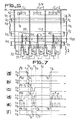
- FIG. 10 represents in its various diagrams (a to d) control signals which can be used in the device represented in FIG. 8.
- control signals are periodic potentials whose amplitude varies between a high level and a low level, denoted respectively V H and V B for all the diagrams, to simplify, these different potentials not necessarily being equal to each other or to potentials of the previous figures.
- Diagram 10a represents the potentials V 41 and V 42 applied to grids G 41 and G 42 ; it is at the low level except during times t 1 , t 2 , t 3 and t 6 , t 7 , t 8 where it is at the high level.
- Diagram 10b represents the potentials V 3 and V 2 applied to the grids G 3 and G 2 : it is at the high level during times t 2 and t 7 .
- Diagram 10c represents the potential V 5 applied to the grid G 5 . It is at low level V B except during times t 1 , t 2 , t 3 and t 4 .
- Diagram 10d represents the potential V 7 applied to the grid G 7 . It is at the low level except during times t 6 , t 7 , t 8 and t 9 , where it is at the high level.
- Diagrams 9b to 9i represent the potential existing on the surface of the semiconductor substrate at different times, shown increasing downwards.
- Diagram 9b represents the surface potential during time t 1 .
- the grid G 2 is at the low level V B and isolates the photosensitive zone from the rest of the device.
- the columns show the quantity of training charges Q. and a quantity of charges Q B coming from a possible over-illumination.
- Diagram 9c represents the surface potential during time t 2 .
- Grid G 2 and grid G 3 are at the high level.
- the quantity of charges Q o + Q B is transferred to the line memory.
- the quantity of charges Q o fills the potential well located under the grid G 41 and the quantity of charges Q B is transferred under the grid G 42 .
- Diagram 9d represents the surface potential during time t 3 .
- the grid G 2 returns to the low level isolating the photosensitive zone from the rest of the device.
- the grid G 3 returns to the low level separating the grids G 41 and G 42 .
- Diagram 9e represents the surface potential during time t 4 .
- the grids G 41 and G 42 go to the low level.
- the quantity of charges Q o is transferred to the columns and the quantity of charges Q B is discharged into the drain D 5 .
- Figure 9f shows the surface potential during time t 5 and t 6 .
- the gate G 5 returns to the low level and isolates the line memory from the drain D 5 .
- a change in level of a clock signal not shown causes the arrival of the quantity of signal charges Q S on the columns. We then have on the columns Q o + Q S.
- FIG. 9g represents the surface potential during time t 7 .
- Grid G 3 goes high which re-establishes communication between grids G 41 and G 42 .
- the grid G 2 goes to high level which allows the transfer of the quantity of charges Q o + Q S coming from the columns in the row memory.
- the quantity of charges Q o is retained under the grid G 41 and the quantity of signal charges Q S passes under the grid G 42 .
- Figure 9h represents the surface potential during time t 8 .
- Grid G 2 returns to the low level, as well as grid G 3 .
- FIG. 9i represents the surface potential during time t 9 .
- the gates G 41 and G 42 pass at the low level which causes on the one hand, the transfer of the quantity of charge-signal Q S in the reading register 32 and on the other hand the transfer of the quantity of charge Q o on the columns.
- the transfer of Q o on the columns at time t 9 explains that at time t 1 the quantity of charge Q o + Q B is found on the columns.
- the generation of the quantity of charges Q o at the level of the line memory is. completely free from spatial noise because this charge is created and then stopped by the same grid receiving the same potential.
- this is the grid G 7 at potential V 7 .
- this is the grid G 3 at the potential V 3 .
- the leakage current is suppressed by applying to the grid G 2 either a voltage continues V 2 , but a signal V 2 which varies periodically between a low level and a high level.
- the signal V 2 is at the low level.
- a significant potential barrier exists between the potential on D 2 and the potential under the grid G 2 .
- the leakage current is then negligible.
- This pulse on G 2 takes place whenever we want to pass charges from the columns to the row memory, whether it is the signal charges at the time of their reading, or the charges coming from a possible over-illumination.
- Q B at the end of line time, for example.
- the amplitude of the pulse on G 2 can be around 1 Volt to effectively reduce the leakage current while it is of the order of 10 to 15 Volts for the other control signals mentioned.
- the grid G 1 is essential in this operating mode. It avoids a parasitic coupling between G 2 and D 2 which. would have the effect of partially maintaining the potential barrier at the time when the impulse is applied to G 2 . Indeed, the diode D 2 tends to follow the potential of G 2 through its coupling capacity with G 2 .
- the above description has been given by way of nonlimiting example.
- the relative position of the grids G 1 , G 5 and G 7 , and of the diodes D 2 and D 5 , as well as their dimensions, have no particular function but derive solely from their technological embodiment.
- the shape of the isolation barriers 43 or 46 is arbitrary, as is the shape of the notches 24 or 26.
Landscapes
- Engineering & Computer Science (AREA)
- Multimedia (AREA)
- Signal Processing (AREA)
- Physics & Mathematics (AREA)
- Power Engineering (AREA)
- General Physics & Mathematics (AREA)
- Condensed Matter Physics & Semiconductors (AREA)
- Electromagnetism (AREA)
- Computer Hardware Design (AREA)
- Microelectronics & Electronic Packaging (AREA)
- Computer Vision & Pattern Recognition (AREA)
- Solid State Image Pick-Up Elements (AREA)
- Transforming Light Signals Into Electric Signals (AREA)
Abstract
Le dispositif selon l'invention comporte principalement: -une matrice (1) de N lignes et M colonnes de points photosensibles (15); -un ensemble (2) comportant une mémoire de ligne de M points recevant en parallèle les charges électriques fournies par les M points d'une même ligne de la matrice photosensible (1), et un dispositif d'évacuation des charges parasites comportant des diodes, cet ensemble assurant l'injection d'une même quantité prédéfinie (Q0) de charges entre chacun des points photosensibles et la sortie du dispositif; - un registre à décalage de sortie (3), recevant en parallèle les charges fournies par la mémoire de ligne et délivrant en série un signal électrique d'analyse de l'image. Ce dispositif est notamment applicable à une caméra de télévision.The device according to the invention mainly comprises: a matrix (1) of N rows and M columns of photosensitive dots (15); an assembly (2) comprising a line memory of M points receiving in parallel the electric charges supplied by the M points of the same line of the photosensitive matrix (1), and a device for removing parasitic charges comprising diodes , this assembly ensuring the injection of the same predefined quantity (Q0) of charges between each of the photosensitive points and the output of the device; - an output shift register (3), receiving in parallel the charges provided by the line memory and delivering in series an electrical image analysis signal. This device is particularly applicable to a television camera.
Description
La présente invention se rapporte au domaine de l'analyse électrique d'images lumineuses en lignes successives, constituant des trames, à l'aide d'un dispositif à transfert de charges comportant une mémoire de ligne.The present invention relates to the field of electrical analysis of light images in successive lines, constituting frames, using a charge transfer device comprising a line memory.
On connaît différents dispositifs à l'état solide pour l'analyse d'une image lumineuse, qui sont destinés à être utilisés dans une caméra de télévision pour fournir un signal électrique vidéo. Ils se distinguent par le mode de réalisation de la zone photosensible d'une part, et le système de lecture et d'évacuation des charges créées par l'image, d'autre part.Various solid state devices are known for analyzing a light image, which are intended to be used in a television camera to provide an electrical video signal. They are distinguished by the embodiment of the photosensitive area on the one hand, and the system for reading and discharging the charges created by the image, on the other hand.
Il est également connu d'utiliser des dispositifs à transfert de charges pour réaliser ces différentes fonctions, comme il est décrit par exemple dans l'ouvrage de SEQUIN et TOMPSETT, intitulé "Charge transfer devices", (pages 152 à 169) :
- - dans des organisations dites "à transfert de trame" ou "à structure interligne", dans lesquelles le rayonnement lumineux est reçu sur des registres à transfert de charges ; dans ces dispositifs, le transfert de charges est réalisé sur de grandes surfaces, ce qui constitue un inconvénient du fait qu'il est actuellement difficile d'obtenir des rendements élevés pour la fabrication de ces grandes surfaces ;
- - dans des dispositifs dits "CID" (pour "Charge Injection Devices") qui ne présentent pas cet inconvénient mais qui nécessitent en général une réinjection des charges dans le substrat semiconducteur, ce qui présente un certain nombre d'inconvénients parmi lesquels du bruit ou des difficultés au niveau des valeurs des capacités nécessaires pendant ou après la lecture des charges.
- - in so-called "frame transfer" or "interline structure" organizations, in which the light radiation is received on charge transfer registers; in these devices, the transfer of charges is carried out over large areas, which constitutes a drawback because it is currently difficult to obtain high yields for the manufacture of these large areas;
- - In so-called "CID" devices (for "Charge Injection Devices") which do not have this drawback but which generally require reinjection of the charges into the semiconductor substrate, which has a number of drawbacks, including noise or difficulties with the values of the capacities required during or after the reading of the loads.
Plus généralement, en sus des problèmes évoqués ci-dessus, se pose la question de la compatibilité des temps nécessaires d'une part à l'intégration lumineuse et d'autre part au transfert des charges dans le cas où cette solution est retenue, avec les temps de balayage de l'écran de télévision qui sont, selon le standard 625 lignes habituel, environ de 52 ps pour le temps d'affichage d'une ligne et de 12 µs pour le temps de retour ligne.More generally, in addition to the problems mentioned above, the question arises of the compatibility of the times required on the one hand for the light integration and on the other hand for the transfer of the charges in the case where this solution is chosen, with the scanning times of the television screen which, according to the usual 625 line standard, are approximately 52 ps for the display time of a line and 12 µs for the line feed time.
Pour répondre à ces différents impératifs, la Demanderesse a proposé une structure dite "à transfert de ligne", décrite dans la demande de brevet français n° 80-09112, qui comporte principalement :
- - une matrice de N lignes x M zones, ou points, photosensibles, matrice sur laquelle une image à lire est projetée et convertie en charges électriques dites charges signal ;
- - une mémoire de M points, dite mémoire de ligne, destinée à recevoir successivement les charges signal stockées par chaque ligne ;
- - un dispositif d'évacuation des charges parasites, associé à la mémoire de ligne ;
- - un registre à décalage du type CCD (pour "Charge Coupled Devices"), recevant en parallèle le contenu de la mémoire de ligne et délivrant en série le signal électrique d'analyse de l'image.
- - a matrix of N lines x M zones, or points, photosensitive, matrix on which an image to be read is projected and converted into electrical charges called signal charges;
- - a memory of M points, called line memory, intended to successively receive the signal charges stored by each line;
- - a device for removing parasitic charges, associated with the line memory;
- - a shift register of the CCD type (for "Charge Coupled Devices"), receiving in parallel the content of the line memory and delivering in series the electrical image analysis signal.
La présente invention a pour objet un dispositif d'analyse d'image du type à transfert de ligne décrit ci-dessus, dans lequel a été perfectionné l'ensemble assurant la mémorisation des lignes successives et l'évacuation des charges parasites, afin d'améliorer le traitement des petits signaux et diminuer le bruit.The present invention relates to an image analysis device of the line transfer type described above, in which the assembly has been perfected ensuring the storage of successive lines and the evacuation of parasitic charges, in order to improve the processing of small signals and reduce noise.
A cet effet, le dispositif selon l'invention comporte :
- - une pluralité de zones photosensibles élémentaires, appelées points, réalisées sur un même substrat semiconducteur selon N lignes et M colonnes et isolées les unes des autres, formant une matrice, dans lesquelles sont créées des charges électriques, dites charges signal, en fonction de l'éclairement reçu ;
- - un ensemble à transfert de charges à M colonnes comportant :
- - une mémoire de M points, dite mémoire de ligne, réalisée dans le même substrat semiconducteur, recevant en parallèle les charges signal fournies par les M points d'une même ligne , la mémoire de ligne comportant une première grille (G,), placée sur le trajet des charges et portée à un potentiel constant (V1), qui assure le découplage de cette grille avec la partie du dispositif située en amont ;
- - un dispositif d'évacuation des charges parasites, comportant une pluralité de diodes et drainant les charges parasites de chacune des colonnes ;
cet ensemble assurant l'injection d'une même quantité prédéfinie de charges dans chacun des points de la mémoire de ligne ; - - un registre à décalage analogique, recevant en parallèle les charges fournies par la mémoire de ligne et délivrant en série un signal électrique d'analyse de l'image.
- - A plurality of elementary photosensitive zones, called points, produced on the same semiconductor substrate along N lines and M columns and isolated from each other, forming a matrix, in which electrical charges, called signal charges, are created as a function of the 'illuminance received;
- - a charge transfer unit with M columns comprising so much:
- - a memory of M points, called line memory, produced in the same semiconductor substrate, receiving in parallel the signal charges supplied by the M points of the same line, the line memory comprising a first grid (G,), placed on the path of the charges and brought to a constant potential (V 1 ), which ensures the decoupling of this grid with the part of the device located upstream;
- - a device for removing parasitic charges, comprising a plurality of diodes and draining the parasitic charges from each of the columns;
this assembly ensuring the injection of the same predefined quantity of charges into each of the points of the line memory; - - an analog shift register, receiving in parallel the charges provided by the line memory and delivering in series an electrical image analysis signal.
L'invention a également pour objet une caméra de télévision comportant un tel dispositif d'analyse d'images.The invention also relates to a television camera comprising such an image analysis device.
L'invention est décrite, à titre d'exemple non limitatif, plus en détail dans ce qui suit à l'aide des figurés annexées, qui représentent :
- - la figure 1, l'organisation générale d'une structure à transfert de ligne ;
- - la figure 2, une vue de dessus d'un premier mode de réalisation du dispositif selon l'invention ;
- - la figure 3 (a à h), une vue en coupe du dispositif de la figure précédente, avec l'illustration des potentiels à différents instants ;
- - la figure 4 (a à f), des signaux susceptibles d'être appliqués au dispositif de la figure 2 ;
- - la figure 5, une vue de dessus d'un deuxième mode de réalisation du dispositif selon l'invention ;
- - la figure 6 (a à h)1 une vue en coupe du dispositif de la figure précédente, avec l'illustration des potentiels à différents instants ;
- - la figure 7 (a à f), des signaux susceptibles d'être appliqués au dispositif de la figure 5 ;
- - la figure 8, une vue de dessus d'un troisième mode de réalisation du dispositif selon l'invention ;
- - la figure 9 (a à i), une vue en coupe du dispositif de la figure précédente, avec l'illustration des potentiels à différents instants ;
- - la figure 10 (a à d), des signaux susceptibles d'être appliqués au dispositif de la figure 8.
- - Figure 1, the general organization of a line transfer structure;
- - Figure 2, a top view of a first embodiment of the device according to the invention;
- - Figure 3 (a to h), a sectional view of the device of the previous figure, with the illustration of the potentials at different times;
- - Figure 4 (a to f), signals that can be applied to the device of Figure 2;
- - Figure 5, a top view of a second embodiment of the device according to the invention;
- - Figure 6 (a to h) 1 a sectional view of the device of the previous figure, with the illustration of the potentials at different times;
- - Figure 7 (a to f), signals that can be applied to the device of Figure 5;
- - Figure 8, a top view of a third embodiment of the device according to the invention;
- - Figure 9 (a to i), a sectional view of the device of the previous figure, with the illustration of the potentials at different times;
- - Figure 10 (a to d), signals that can be applied to the device of Figure 8.
Sur ces différentes figures, les mêmes références se rapportent aux mêmes éléments.In these different figures, the same references relate to the same elements.
La figure 1 représente donc l'organisation générale d'une structure à transfert de lignes, telle que décrite dans la demande de brevet français précitée.FIG. 1 therefore represents the general organization of a line transfer structure, as described in the aforementioned French patent application.
Cette structure comporte principalement une zone photosensible 1, une mémoire de ligne 2 et un registre analogique à décalage de sortie 3.This structure mainly comprises a
La zone photosensible 1 reçoit l'image lumineuse à analyser et la transforme en charges électriques, dites charges signal. Il est à noter qu'on vise ici par image luminepse, la détection non seulement des longueurs d'onde visibles mais également de celles qui les entourent, notamment dans l'infrarouge. La zone photosensible est constituée par une pluralité de zones élémentaires 15, également appelées ci-dessous points, arrangées en N lignes, repérées L1, L2...LN et M colonnes, repérées C1, C2...CM, et formant une matrice. Les points photosensibles d'une même ligne sont reliés entre eux et reliés à un dispositif de commande 14, permettant d'adresser les lignes les unes après les autres ; ce dispositif est constitué par exemple par un registre à décalage. du type MOS. Les points photosensibles 15 d'une même colonne sont reliés à une même connexion, dite ci-après connexion de colonne, vers la mémoire de ligne 2.The
La mémoire de ligne 2 reçoit donc en parallèle les charges signal créées dans chacun des points photosensibles 15 d'une même ligne, puis elle les transfère également en parallèle vers le registre 3. Associés à la mémoire de ligne 2, sont également prévus un dispositif de remise à niveau (connexion RAN sur la figure) des connexions de colonne et un dispositif d'élimination des charges parasites (non représenté sur la figure 1).The
Le registre 3 est un registre à décalage analogique qui fournit l'information, reçue en parallèle, en mode série. Cette information constitue le signal vidéo d'analyse de l'image optique reçue sur la zone photosensible 1. Le registre est de préférence à transfert de charges, de type CCD.
L'enchaînement des différentes opérations d'intégration de l'image au niveau de la zone photosensible 1, du transfert des lignes dans la mémoire de ligne 2, puis du transfert des signaux dans le registre 3, pour les différentes lignes, est réalisé de la façon suivante.The sequence of the various operations of integration of the image at the level of the
Tout d'abord, il est à noter que l'intégration de l'image est réalisée en permanence sur la totalité de la matrice photosensible 1, sauf sur celle des lignes qui est adressée par le registre 14.First of all, it should be noted that the integration of the image is carried out permanently on the whole of the
Pendant le temps de retour ligne, le contenu de la mémoire de ligne 2 est transféré dans le registre à décalage 3, l'entrée de la mémoire de ligne étant alors fermée.During the line return time, the content of the
Pendant le temps ligne qui suit, le contenu du registre 3 est évacué en série, la connexion entre la mémoire de ligne 2 et le registre 3 est interrompue. Pendant ce temps, il se produit, dans une première phase, une remise à niveau des moyens de lecture des points 15 (connexion RAN), reliée à la mémoire de ligne 2 et, dans une deuxième phase, on opère le transfert de l'une des lignes L de la zone 1 vers la mémoire de ligné 2, la sélection (ou "adressage") d'une ligne étant assurée par le registre 14.During the following line time, the content of
L'étape suivante correspond au temps de retour ligne pendant lequel s'opère le déversement du contenu de la mémoire de ligne 2 dans le registre 3, celui-ci ayant été entièrement lu lors de l'étape précédente.The next step corresponds to the line feed time during which the content of the
Dans un autre mode de réalisation, la sélection d'une ligne, son transfert dans la mémoire de ligne puis dans le registre à décalage s'effectuent entièrement pendant le temps de retour ligne, le temps de ligne étant réservé à la remise à niveau des moyens de lecture, qui est d'autant meilleure qu'elle est plus longue, et à l'évacuation en série du registre à décalage.In another embodiment, the selection of a line, its transfer to the line memory and then to the shift register is carried out entirely during the line return time, the time line being reserved for the updating of the reading means, which is all the better the longer it is, and for the serial evacuation of the shift register.
La figure 2 représente une vue de dessus d'un premier mode de réalisation du dispositif selon l'invention.FIG. 2 represents a top view of a first embodiment of the device according to the invention.
Sur cette figure, on a représenté des connexions en provenance des M colonnes C de la matrice photosensible (Ci-1, Ci, Ci+1 sur la figure) aboutissant chacune dans une diode D2, dite diode de réception des charges signal (Qsi) en provenance de la matrice ; elle est réalisée par exemple par dopage d'un substrat semiconducteur qui est avantageusement le même que celui sur lequel est réalisée la matrice photosensible 1. Le dispositif comporte donc M colonnes de transfert de charges, délimitées par des barrières d'isolement 42, correspondant respectivement aux M connexions de colonne de la matrice photosensible.In this figure, connections have been shown coming from the M columns C of the photosensitive matrix (C i-1 , C i , C i + 1 in the figure) each ending in a diode D 2 , called charge reception diode signal (Q si ) from the matrix; it is produced for example by doping a semiconductor substrate which is advantageously the same as that on which the photosensitive matrix is produced 1. The device therefore comprises M charge transfer columns, delimited by
Les diodes D2 sont alignées et sont inférieurement adjacentes à une électrode, ou grille, G1 en forme de bande, qui a pour fonction de constituer un écran pour les charges entre les diodes D2 et le reste du dispositif représenté sur la figure 2, ce qui permet d'éviter l'envoi de charges parasites sur les connexions de colonne C : en effet, dans les dispositifs à transfert de charges, il est particulièrement important de se protéger contre les charges parasites dont l'amplitude peut varier d'un point à l'autre du circuit selon les variations géométriques des éléments et qui limitent la dynamique du signal. A cet effet, la grille G1 est reliée à un potentiel constant V1.The diodes D 2 are aligned and are below adjacent to an electrode, or grid, G 1 in the form of a strip, which has the function of constituting a screen for the charges between the diodes D 2 and the rest of the device represented in FIG. 2 , which avoids the sending of parasitic charges on the column C connections: in fact, in charge transfer devices, it is particularly important to protect against parasitic charges, the amplitude of which can vary from a point to the other of the circuit according to the geometrical variations of the elements and which limit the dynamics of the signal. To this end, the gate G 1 is connected to a constant potential V 1 .
Après la grille écran G1, on trouve une grille G2, en forme de bande parallèle à G,, portée à un second potentiel noté V2, qui a pour fonction de fixer le potentiel des connexions de colonne.After the screen grid G 1 , there is a grid G 2 , in the form of a strip parallel to G ,, brought to a second potential denoted V 2 , which has the function of fixing the potential of the column connections.
Ensuite, on trouve une grille G4 dont la fonction est de stocker les charges, qui est en forme de bande présentant des échancrures 24, par exemple rectangulaires, entre deux colonnes et une colonne sur deux. Dans au moins une partie de chacune de ces échancrures 24 est réalisée une diode D5, ayant pour fonction l'éva- cuation des charges parasites ; les diodes D5 sont reliées à un potentiel VD5 périodique.Next, there is a grid G 4 whose function is to store the charges, which is in the form of a
On verra sur la figure 3 que la grille G2 est entourée de deux grilles coplanaires G1 et G4. Ainsi la largeur de la grille G2 est déterminée en une seule opération de photogravure par l'intervalle entre les grilles Gl et G4. On obtient donc une meilleur homogénéité sur la largeur de la grille G2 qui peut être rendue beaucoup plus petite.It will be seen in FIG. 3 that the grid G 2 is surrounded by two coplanar grids G 1 and G 4 . Thus the width of the grid G 2 is determined in a single photoengraving operation by the interval between the grids G l and G4. A better homogeneity is therefore obtained over the width of the grid G 2 which can be made much smaller.
Ainsi, sont éliminés les parasites susceptibles d'être introduits par une pénétration variable d'un point photosensible à l'autre des diodes D2 sous la grille G2. Cette pénétration variable peut conduire à des temps de transfert variables des charges-signal de chaque diode D2 vers la mémoire en raison de la largeur variable de la grille du transistor MOS équivalent à travers lequel se fait le transfert des charges en mémoire ; de plus, ce mode de réalisation présente l'avantage d'augmenter la rapidité du transfert des charges-signal de D1 et D2 en mémoire, à cause de la diminution de la largeur de G2.Thus, the parasites liable to be introduced are eliminated by variable penetration from one photosensitive point to the other of the diodes D 2 under the grid G2. This variable penetration can lead to variable transfer times of the signal charges from each diode D 2 to the memory due to the variable width of the gate of the equivalent MOS transistor through which the charges are transferred to the memory; in addition, this embodiment has the advantage of increasing the speed of the transfer of the signal charges from D 1 and D 2 into memory, because of the reduction in the width of G 2 .
Le dispositif comporte encore une grille G5 en forme de bande, recouvrant la grille de stockage G4, par l'intermédiaire d'une couche d'isolant, au niveau des échancrures 24, de façon à être adjacente supérieurement aux diodes D5 ; la grille G5 reçoit un potentiel périodique V5 et permet de commander l'accès des charges aux diodes D5.The device also comprises a grid G 5 in the form of a strip, covering the storage grid G 4 , by means of an insulating layer, at the level of the
Parallèle à la grille G5 et recouvrant légèrement la partie inférieure des diodes D5, on trouve une grille G7, à laquelle est appliqué un potentiel périodique V7, permettant de commander l'accès au registre à décalage 3.Parallel to the grid G 5 and slightly covering the lower part of the diodes D5, there is a grid G 7 , to which a periodic potential V 7 is applied, making it possible to control access to the
Les barrières d'isolement 42 s'interrompent au niveau des échancrures 24 ou se terminent, dans le cas où il n'y a pas d'échancrure, par un élargissement, par exemple en forme de triangle 43. Les diodes D5 sont entourées par une barrière d'isolement 44 en forme de U, de telle sorte que la diode D5 reste accessible aux charges en provenance des diodes D2 de chacune des colonnes. De la sorte sont définis deux canaux par colonne : un premier canal, noté CL1, limité par une barrière d'isolement 42, son élargissement 43, et une branche du U 44 côté extérieur, et un second canal, noté CL2, limité par le côté intérieur du même U 44 et la seconde barrière d'isolement 42 limitant la colonne considérée.The
Le registre 3 est un registre C.C.D. à deux phases ∅1 et ∅2. Il est constitué par deux séries d'électrodes de stockage (31, 32) et deux séries d'électrodes de transfert (33, 34), toutes de forme sensiblement rectangulaire, et placées perpendiculairement aux grilles G1 à G7 précédentes. Les grilles 31 sont reliées au potentiel périodique ∅1 et les grilles 32, au potentiel périodique ∅2; les grilles 33 et 34 sont placées respectivement entre les couples de grilles 32-31 et 31-32, dans le sens de transfert des charges, sur une surépaisseur d'isolant et sont reliées respectivement aux potentiels ∅1 et ∅2. En outre, les électrodes du registre 3 sont placées de telle sorte que les électrodes 31 prennent naissance sur les barrières d'isolement 43 ou 44, les électrodes 32 se trouvant dans le prolongement des canaux CL1. Le registre 3 est limité inférieurement par une barrière d'isolement horizontale 44, comme le dispositif est limité supérieurement par une barrière d'isolement également horizontale 41.
Dans ce mode de réalisation, comme dans les suivants, les différentes barrières d'isolement décrites ci-dessus ou ci-après peuvent être réalisées de toute façon connue, telle qu'un surdopage du substrat, d'un même type de conductivité que ce dernier, ou une surépaisseur localisée de la couche isolante (en général oxyde) recouvrant le substrat, cette dernière solution pouvant être accompagnée d'un surdopage du substrat réalisé sous la surépaisseur d'isolement. Les différentes électrodes peuvent être réalisées également de toute façon connue : métal ou silicium polycristallin par exemple. Enfin, afin d'éviter la création de charges parasites, chaque diode et une partie des grilles voisines est recouverte d'une couche opaque aux rayons lumineux, telle qu'une couche d'aluminium.In this embodiment, as in the following, the various isolation barriers described above or below can be produced in any known way, such as an overdoping of the substrate, of the same type of conductivity as that last, or a localized excess thickness of the insulating layer (in general oxide) covering the substrate, the latter solution being able to be accompanied by an overdoping of the substrate produced under the insulation excess thickness. The various electrodes can also be produced in any known way: metal or polycrystalline silicon for example. Finally, in order to avoid the creation of parasitic charges, each diode and part of the neighboring grids is covered with a layer opaque to light rays, such as a layer of aluminum.
La figure 3a représente une vue en coupe du dispositif de la figure 2, et les diagrammes 3b à 3h, l'illustration du potentiel de surface dans le substrat semiconducteur à différents instants, le potentiel de surface étant représenté sur ces diagrammes comme sur les suivants croissant vers le bas.Figure 3a shows a sectional view of the device of the FIG. 2, and diagrams 3b to 3h, the illustration of the surface potential in the semiconductor substrate at different times, the surface potential being represented on these diagrams as on the following ones increasing downwards.
Pour faciliter la compréhension du fonctionnement du dispositif, on a représenté sur le schéma de la figure 3a une coupe réalisée à différents endroits.To facilitate understanding of the operation of the device, there is shown in the diagram of Figure 3a a section made in different places.
A gauche d'un axe XX, on a figuré un point photosensible de la matrice 1. A titre d'exemple, il est constitué par une grille GL constituant une électrode d'une capacité MOS photodétectrice, portée à un potentiel périodique VGL, recouvrant légèrement la grille qui la suit, repérée GE, qui est un écran pour les charges, séparant la zone photosensible proprement dite de la connexion de colonne, et qui est portée à un potentiel VGE constant ; la grille écran GE est suivie par une diode de lecture DL, réalisée dans le substrat, point de départ de la connexion de colonne ci. Dans une variante de réalisation, non représentée, le point photosensible comporte une seconde zone de détection de l'image lumineuse, dont la sensibilité en fréquence est complémentaire de la capacité MOS, réalisée par exemple par une photodiode.To the left of an axis XX, a photosensitive point of the matrix has been represented. By way of example, it is constituted by a grid G L constituting an electrode of a photodetector MOS capacity, brought to a periodic potential V GL , slightly covering the grid which follows it, marked G E , which is a screen for the charges, separating the photosensitive zone proper from the column connection, and which is brought to a constant potential V GE ; the screen grid G E is followed by a reading diode D L , produced in the substrate, starting point of the column connection c i . In an alternative embodiment, not shown, the photosensitive point comprises a second zone for detecting the light image, the frequency sensitivity of which is complementary to the MOS capacity, produced for example by a photodiode.
On a figuré à droite de l'axe XX une coupe réalisée dans le dispositif de la figure 2 selon une ligne AA passant par la diode D2, la grille Gl, la grille G4 et le second canal CL2, la grille G4 étant alors suivie par la grille G5 qui la recouvre légèrement, G5 étant elle-même suivie par la diode D5 ; il apparaît sur cette figure que la grille G2 recouvre légèrement les grilles qui l'entourent : G1 et G4' On a également figuré la connexion de colonne c. reliant les diodes DL et D2.There is shown to the right of the axis XX a section made in the device of FIG. 2 along a line AA passing through the diode D 2 , the grid G l , the grid G 4 and the second channel CL 2 , the grid G 4 then being followed by the grid G 5 which covers it slightly, G 5 itself being followed by the diode D5; it appears in this figure that the grid G 2 slightly covers the grids which surround it: G 1 and G 4 ' We have also shown the connection of column c. connecting the diodes D L and D 2 .
Après la diode D5 a été figurée sur le schéma une coupe réalisée, dans le dispositif de la figure 2 selon une ligne BB, le long du premier canal CL1, coupe séparée sur la figure 3a de ce qui précède par un axe YY. La coupe du premier canal commence au niveau de la grille G4 et se poursuit jusqu'à une électrode 32 du registre 3, G4 et 32 étant séparées par la grille G7 qui les recouvre légèrement l'une et l'autre. Il est à noter que, dans ce mode de réalisation comme dans les suivants, le fonctionnement du dispositif est compatible avec un transfert de charges dit "en volume" dans le registre de sortie 3. Ainsi qu'il est connu, le transfert de charges dans le volume du substrat semiconducteur est plus rapide que le transfert en surface, et son efficacité est meilleure ; le transfert en volume se distingue du transfert en surface principalement par :
- - des potentiels appliqués plus élevés ;
- --un dopage de la partie du substrat semiconducteur où s'opère le transfert d'un type de conductivité opposé à celui du reste du substrat.
- - higher applied potentials;
- - doping of the part of the semiconductor substrate where the transfer takes place of a conductivity type opposite to that of the rest of the substrate.
Sur les figures, on a représenté à titre d'exemple un fonctionnement en transfert en volume, et donc une zone dopée (hachurée) notée T.V. s'étendant sous les électrodes du registre 3 jusqu'à la moitié de la grille G7.In the figures, an operation in volume transfer is shown by way of example, and therefore a doped (hatched) area denoted TV extending under the electrodes of
Ces différents éléments sont réalisés de préférence sur un même substrat semiconducteur 21, recouvert d'une couche d'isolant non représentée, les différentes électrodes étant séparées, lorsqu'elles se recouvrent, par une couche d'isolant, également non représentée pour la clarté du schéma.These different elements are preferably produced on the
La figure 4 représente dans ses différents diagrammes (a à e) l'évolution dans le temps des signaux de commande appliqués au dispositif de la figure 3.FIG. 4 shows in its various diagrams (a to e) the evolution over time of the control signals applied to the device of FIG. 3.
Le diagramme.4a représente le potentiel VGL qui est à un niveau haut (VH) constant, sauf pendant un intervalle de temps T4 à T7, qui correspond au temps de transfert des charges accumulées dans le point photosensible considéré vers la mémoire de ligne puis le registre 3 de la figure 2, et qui correspond sensiblement au temps de retour ligne.Diagram 4a represents the potential V GL which is at a constant high level (V H ), except during a time interval T 4 to T 7 , which corresponds to the transfer time of the charges accumulated in the photosensitive point considered towards the memory line then register 3 of Figure 2, and which corresponds substantially to the line return time.
Le diagramme 4b représente le potentiel V4 qui est a un niveau haut (VH) constant, sauf entre des instants T3 et T5 encadrant l'instant T4 précédent.Diagram 4b represents the potential V 4 which is at a constant high level (V H ), except between instants T 3 and T5 framing the instant T 4 above .
Le diagramme 4c représente le potentiel V5 qui est à un niveau haut (VH) jusqu'à un instant To auquel il passe à un niveau intermédiaire (VI) où il reste jusqu'à un instant T2, T0 et T2 étant antérieurs à l'instant T3 précédent. A partir de l'instant T2, V5 reste à un niveau bas (VB) jusqu'à un instant T8, postérieur à l'instant T7, auquel il remonte au niveau haut VH.Diagram 4c represents the potential V 5 which is at a high level (V H ) until an instant T o at which it passes to a level intermediate (V I ) where it remains until an instant T 2 , T 0 and T 2 being prior to the previous instant T 3 . From the instant T 2 , V5 remains at a low level (V B ) until an instant T 8 , posterior to the instant T 7 , to which it rises to the high level V H.
Le diagramme 4d représente le potentiel VD5 qui est à un niveau haut (VH) constant sauf entre l'instant T0 et un instant T1 compris entre T0 et T2, durée pendant laquelle il est à un niveau bas (VB).Diagram 4d represents the potential V D5 which is at a constant high level (V H ) except between the instant T 0 and an instant T 1 between T 0 and T 2 , duration during which it is at a low level (V B ).
Le diagramme 4e représente le potentiel V7 qui est à un niveau bas constant, sauf entre un instant T6, antérieur à l'instant T7, et T7, durée pendant laquelle il est à un niveau haut (VH).Diagram 4e represents the potential V 7 which is at a constant low level, except between an instant T 6 , prior to the instant T 7 , and T 7 , duration during which it is at a high level (V H ).
En se reportant au diagramme 3b, à un instant t0 compris entre les instants T0 et T1, la diode D5 est au niveau bas, ce qui permet l'injection de charges sous la grille G4, cette injection étant limitée par le potentiel constant V2 appliqué sur la grille G2, ce qui implique que le niveau bas de VD5 soit supérieur au potentiel V2. Il apparaît ainsi que la grille G2 fixe le niveau du potentiel des connexions de colonne ci. Par ailleurs, à gauche de la ligne XX, une quantité de charge signal Qsi est présente sous la grille GL (zone hachurée).Referring to diagram 3b, at a time t 0 between the instants T 0 and T 1 , the diode D 5 is at the low level, which allows the injection of charges under the gate G 4 , this injection being limited by the constant potential V 2 applied to the grid G 2 , which implies that the low level of V D5 is greater than the potential V 2 . It thus appears that the grid G 2 fixes the level of the potential of the column connections c i . Furthermore, to the left of line XX, a quantity of signal charge Q si is present under the grid G L (hatched area).
Le diagramme de la figure 3c représente les potentiels à un instant t1 compris entre T1 et T2. A cet instant, le potentiel VD5 est au niveau haut et, de ce fait, une quantité de charge Q0 se trouve isolée sous la grille G4 (zone hachurée) par les potentiels V2 et V5 appliqués respectivement sur les grilles G2 et G5. Cette quantité de chargé Q0 dépend du potentiel VI qui est alors appliquée sous la grille G5, le potentiel V2 étant supposé plus faible que VI.The diagram in FIG. 3c represents the potentials at an instant t 1 between T 1 and T 2 . At this instant, the potential V D5 is at the high level and, therefore, a quantity of charge Q 0 is isolated under the grid G 4 (hatched area) by the potentials V 2 and V 5 applied respectively to the grids G 2 and G 5 . This quantity of charge Q 0 depends on the potential V I which is then applied under the gate G 5 , the potential V 2 being assumed to be lower than V I.
A un instant t2, compris entre T3 et T4, les tensions V4 et V5 sont ramenées au niveau bas, ce qui a pour effet de transférer la quantité de charge Q0 sur les diodes D2 et, par l'intermédiaire de la connexion ci, sur les diodes DL. Ceci est représenté par une flèche 51 sur la partie du diagramme 3d qui est comprise entre les lignes XX et YY.At an instant t 2 , between T3 and T 4 , the voltages V 4 and V 5 are brought back to the low level, which has the effect of transferring the quantity of charge Q 0 on the diodes D 2 and, via of the connection c i , on the diodes D L. This is represented by an
A un instant ultérieur noté t3, situé entre T4 et T5, le potentiel appliqué à la grille GL de la capacité MOS de la zone photosensible est porté au niveau bas, ce qui a pour effet de transférer la quantité de charge Qsi vers les diodes DL (flèche 52 sur la partie gauche de la figure 3d).At a later instant noted t 3 , located between T4 and T 5 , the poten tiel applied to the grid G L of the MOS capacity of the photosensitive zone is brought to the low level, which has the effect of transferring the amount of charge Q if to the diodes D L (
Le diagramme 3e représente la situation à un instant t4, entre les instants T5 et T6. Pendant cette période, le potentiel appliqué sur la grille G4 est porté au niveau haut, ce qui permet le transfert (flèche 53) des charges Q0 + Qsi sous la grille G4, et ce dans les deux canaux, ce-qui est illustré à droite et à gauche de l'axe YY.The diagram 3e represents the situation at an instant t4, between the instants T 5 and T 6 . During this period, the potential applied to the grid G4 is brought to the high level, which allows the transfer (arrow 53) of the charges Q 0 + Q if under the grid G 4 , and this in the two channels, which is shown to the right and left of the YY axis.
Le diagramme 3f représente la situation à un instant t5 situé entre T6 et T7, période pendant laquelle les potentiels du canal CL2 sont inchangés, mais la grille G7 placée sur le canal CL1 voit son potentiel augmenter, ce qui permet le transfert (flèche 54) des charges Q0 + Qsi présentes sous la grille G4 vers le registre à décalage 3, matérialisé par une de ses électrodes 32. Il .apparaît ainsi que la quantité de charge connue QO est effectivement transférée dans le registre 3, en même temps que la charge signal Qsi.Diagram 3f represents the situation at an instant t 5 situated between T6 and T 7 , period during which the potentials of channel CL 2 are unchanged, but the grid G 7 placed on channel CL 1 sees its potential increasing, which allows the transfer (arrow 54) of the charges Q 0 + Q if present under the gate G 4 towards the
En général, on évite le transfert de cette charge Q0 dans le registre 3, en ne transférant alors que la charge signal Qsi, ce qui permet d'éliminer le bruit dit spatial sur Q0 d'une colonne à l'autre, bruit dû à des variations de charges introduites par des variations de l'épaisseur de l'oxyde recouvrant le substrat, une variation des tensions de seuil, etc. Ceci peut être réalisé en portant la grille G7 à un potentiel intermédiaire VI, représenté sur le diagramme 4f, dont l'amplitude est comprise entre VB et VHI pendant les instants T6 à T7, la valeur VI de ce potentiel intermédiaire étant avantageusement égale au potentiel intermédiaire appliqué sur la grille G5 entre les instants T0 et T2. On obtient alors un fonctionnement décrit par le diagramme 3g où l'on voit que le potentiel appliqué sur la grille G7 est tel que seule la charge signal Qsi (flèche 55) peut être transférée de la grille G4 à l'électrode 32 pardessus la grille G7, la charge Q0 restant sous la grille G4. Il est à noter que, dans cette variante, la phase correspondant au diagramme 3b peut être supprimée : en effet, cette étape est une étape d'injection de la charge Q0 dans le dispositif qui n'est plus nécessaire du fait que cette charge n'est plus éliminée.In general, the transfer of this charge Q 0 in the
Ce qui est essentiel est que le transfert des charges-signal Qsi des diodes D2 sous la grille G2 puis sous la grille G4 se fasse en superposant à la quantité de charges-signal Qsi une quantité de charges Qo car la capacité des diodes D2 est très importante. Par contre le transfert des charges-signal Qsi vers le registre de lecture peut se faire sans adjonction de la quantité de charges Qo car la capacité présentée par la grille G4 est faible et du même ordre que celle du registre.What is essential is that the transfer of charge-signal Q if diodes D 2 under the gate G 2 then under the gate G 4 is done by superimposing on the quantity of charge-signal Q if a quantity of charges Q o because the capacity of the diodes D 2 is very important. On the other hand, the transfer of the signal Q charges if to the reading register can be done without adding the quantity of charges Q o because the capacity presented by the grid G 4 is low and of the same order as that of the register.
A un instant t6, ultérieur à l'instant T8 et situé n'importe où pendant le temps ligne, le potentiel appliqué sur la grille G5 étant porté au niveau haut VH, il y a élimination de toute charge parasite (QB) provenant d'une connexion de colonne, par le canal CL2 vers la diode D5. Ces charges parasites proviennent par exemple des points suréclairés de la matrice photosensible.At an instant t 6 , subsequent to the instant T 8 and located anywhere during the line time, the potential applied to the gate G 5 being brought to the high level V H , there is elimination of any parasitic charge (Q B ) coming from a column connection, via channel CL 2 to diode D 5 . These parasitic charges originate, for example, from points which are over-lit in the photosensitive matrix.
Si l'on se reporte aux diagrammes 4f et 3g, il est nécessaire qu'à l'instant t6, le potentiel appliqué sur la grille G5 soit égal non plus à VH mais au niveau intermédiaire VI, afin de conserver la seule charge QO sous la grille G4, et d'éliminer par D5 d'éventuelles charges parasites.If we refer to diagrams 4f and 3g, it is necessary that at time t 6 , the potential applied to the grid G 5 is no longer equal to V H but at the intermediate level V I , in order to preserve the single charge Q O under the grid G 4 , and to eliminate by D 5 any parasitic charges.
Dans ce cas, le bruit spatial résiduel ne peut être dû qu'à des variations de seuil, de dopage ou d'épaisseur d'isolant entre les grilles G7 et G5, ce qui est très minime dans la pratique, compte tenu de la proximité géométrique de ces deux grilles.In this case, the residual spatial noise can only be due to variations in threshold, doping or thickness of insulation between the gates G 7 and G 5 , which is very minimal in practice, taking into account the geometric proximity of these two grids.
Cette structure permet donc d'injecter une quantité Q0 prédéterminée de charges d'abord sous la grille de stockage G4, puis sur les diodes DL et D2 établissant la connexion entre la matrice photosensible et la mémoire de ligne, afin d'améliorer le transfert des charges signal Qsi. Cette quantité de charges Q0 est ainsi injectée en utilisant la structure de la mémoire de ligne et du dispositif d'élimination des charges parasites, et donc sans nécessiter de dispositif auxiliaire.This structure therefore makes it possible to inject a predetermined quantity Q 0 of charges first under the storage grid G 4 , then on the diodes D L and D 2 establishing the connection between the photosensitive matrix and the line memory, in order to improve signal transfer charge Q if . This quantity of charges Q 0 is thus injected using the structure of the line memory and of the device for eliminating parasitic charges, and therefore without requiring an auxiliary device.
En outre, dans ce mode de réalisation, chaque diode d'évacuation des charges parasites (D5) est commune à deux colonnes, ce. qui permet soit d'augmenter la capacité de stockage de la mémoire de ligne (grille G4 plus étendue), soit de permettre un pas horizontal plus réduit et donc un encombrement moindre du dispositif.In addition, in this embodiment, each diode for discharging parasitic charges (D 5 ) is common to two columns, this. which makes it possible either to increase the storage capacity of the line memory (more extensive grid G 4 ), or to allow a smaller horizontal pitch and therefore a smaller footprint of the device.
La figure 5 représente une vue de dessus d'un deuxième mode de réalisation de l'invention où la génération de la quantité de charge QO est complètement exempte de bruit spatial.FIG. 5 represents a top view of a second embodiment of the invention where the generation of the quantity of charge Q O is completely free of spatial noise.
Sur cette figure, on retrouve les diodes D2, la grille G1, la grille G2 et la grille G4, mais qui maintenant présente une échancrure 25 au niveau de chacune des colonnes, échancrures dans chacune desquelles est placée comme précédemment une diode D5. Les grilles G5 et G7 sont placées parallèlement aux autres grilles, de part et d'autre des diodes D5. Perpendiculairement aux précédentes, on retrouve les électrodes 31 à 34 du registre 3.In this figure, we find the diodes D 2 , the grid G 1 , the grid G 2 and the grid G 4 , but which now has a
On retrouve également les barrières d'isolement verticales 42 entre les colonnes, allant jusqu'aux électrodes 34 du registre 3 ; en outre, chacune des colonnes est divisée verticalement par une barrière d'isolement 45, délimitant à sa gauche un premier canal repéré CL1, allant de la grille G4 à une électrode 32, à sa droite un second canal repéré CL2 et contenant la diode D5, qui s'étend alors entre les barrières 45 et 42, et enfin un troisième canal, repéré CL3, allant de l'électrode 31 du registre 3 vers la diode D5, c'est-à-dire opposé au canal CL2.We also find the
La.figure 6a représente, à gauche d'un axe ZZ, une coupe selon une ligne fermée CC, réalisée à partir de la diode D5 autour de la barrière d'isolement 45 de la figure 5, et à droite de l'axe ZZ, une coupe réalisée selon une ligne DD de la grille G4 à la diode D2, ces deux coupes étant réunies sur le même schéma pour la clarté de l'explication du fonctionnement du dispositif de la figure 5.La.figure 6a represents, on the left of an axis ZZ, a section along a closed line CC, produced from the diode D5 around the
On trouve donc sur la figure 6a, successivement en partant de la gauche, le canal CL2 représenté par la diode D5, la grille G5 recouvrant légèrement la grille G4 qui la suit, la grille G4 étant commune aux canaux CL2 et CL,, puis le canal CL1 représenté par la grille 32, séparée de la- grille G4 par la grille G7 qui les recouvre légèrement toutes les deux ; la grille 31 séparée de la grille 32 par la grille 33 qui les recouvre légèrement et qui fait la séparation entre les canaux CL1 et CL3, puis le canal CL3 constitué par la grille G7 et la diode D5. A droite de la ligne ZZ, on trouve successivement la grille G4, la grille G1 séparée de la précédente par la grille G2 qui les recouvre légèrement, puis la diode D2 qui reçoit la connexion de colonne Ci.We therefore find in FIG. 6a, successively from the left, the channel CL 2 represented by the diode D5, the grid G 5 slightly covering the grid G 4 which follows it, the grid G 4 being common to the channels CL 2 and CL ,, then the channel CL 1 represented by the
Comme précédemment, on a représenté une zone de dopage s'étendant de la grille G7 aux électrodes 31, 32 et 33 du registre 3, correspondant au fonctionnement de type transfert en volume de ce registre.As before, a doping zone has been shown extending from the gate G 7 to the
La figure 7 représente dans ses différents diagrammes (a à f), l'évolution dans le temps des différents signaux de commande appliqués au dispositif de la figure 5, ces signaux de commande étant des potentiels périodiques dont l'amplitude varie entre un niveau bas, noté VB pour tous les diagrammes, et un niveau haut, noté VH également pour tous les diagrammes, pour simplifier, ces différents potentiels n'étant pas forcément égaux.FIG. 7 represents in its different diagrams (a to f), the evolution over time of the different control signals applied to the device of FIG. 5, these control signals being periodic potentials whose amplitude varies between a low level , denoted VB for all the diagrams, and a high level, denoted V H also for all the diagrams, for simplicity, these different potentials are not necessarily equal.
Le diagramme 7a représente le potentiel V5 qui est à un niveau haut, sauf à partir d'un instant T2 jusqu'à un instant T8, la durée T2.T8 étant sensiblement celle du retour ligne.Diagram 7a represents the potential V 5 which is at a high level, except from an instant T 2 until an instant T 8 , the duration T 2 .T 8 being substantially that of line return.
Le diagramme 7b représente le potentiel VD5 qui est à un niveau haut, sauf entre deux instants T1 et T3, encadrant l'instant T2 précédent, où il est à un niveau bas.Diagram 7b represents the potential V D5 which is at a high level, except between two instants T 1 and T 3 , framing the instant T 2 above , where it is at a low level.
Le diagramme 7c représente le potentiel V7 qui est à un niveau bas jusqu'à un instant T4 postérieur à l'instant T3 auquel il passe à un niveau haut, jusqu'à un instant T5 postérieur, où il repasse au niveau bas, jusqu'à un instant T6 postérieur, où il repasse au niveau haut jusqu'en T8, où il repasse au niveau bas.Diagram 7c represents the potential V 7 which is at a low level until an instant T 4 posterior to the instant T3 at which it passes to a high level, until an instant T 5 posterior, where it returns to the low level , until a later time T 6 , where it returns to the high level until T 8 , where it returns to the low level.
Le diagramme 7d représente le potentiel ∅2 qui est un signal en crénaux de période T jusqu'à un instant To antérieur à l'instant T1 auquel il passe à un niveau haut jusqu'à l'instant T5 auquel il passe à un niveau bas qu'il conserve jusqu'à l'instant T6 auquel il passe à un niveau haut jusqu'à l'instant T8 où il redevient un signal en crénaux de même période que précédemment.Diagram 7d represents the potential ∅ 2 which is a signal in time slots of period T up to an instant T o prior to the instant T 1 at which it goes high until the instant T 5 at which it goes to a low level which it maintains until time T 6 at which it passes to a high level until time T 8 where it becomes again a signal in time slots of the same period as previously.
Le digramme 7e représente le potentiel ∅1 qui est complémentaire du signal ∅2.The diagram 7e represents the potential ∅ 1 which is complementary to the signal ∅ 2 .
Le diagramme 7f représente le potentiel V4 qui est à un niveau haut jusqu'à l'instant T5 où il passe à un niveau bas jusqu'à un instant T7 compris entre T6 et T8, instant auquel il repasse au niveau haut.Diagram 7f represents the potential V 4 which is at a high level until the instant T 5 where it passes to a low level until an instant T 7 between T 6 and T 8 , instant at which it returns to the level high.
La figure 6b représente le potentiel de surface dans le semiconducteur au niveau de la figure 6a, à un instant to compris entre T1 et T2. Pour la clarté de la lecture de ce diagramme et des suivants, on a figuré sur chacun d'eux la surface du substrat semiconducteur, repérée 22. A cet instant tO, le potentiel VD5 appliqué sur la diode D5 est au niveau bas alors que le potentiel V5 appliqué sur la grille G5 est au niveau haut, ce qui autorise l'envahissement par les charges de la zone située sous la grille G4, cet envahissement (zone hachurée) étant limité par la grille G7 portée au potentiel V7 qui est au niveau bas.FIG. 6b represents the surface potential in the semiconductor at the level of FIG. 6a, at an instant t o comprised between T 1 and T 2 . For the clarity of the reading of this diagram and the following ones, one has figured on each of them the surface of the semiconductor substrate, marked 22. At this instant t O , the potential V D5 applied to the diode D 5 is at the low level while the potential V 5 applied to the grid G 5 is at the high level, which allows the invasion by the charges of the area located under the grid G 4 , this invasion (hatched area) being limited by the grid G 7 carried at potential V 7 which is at the low level.
La figure 6c représente le potentiel de surface à un instant tl, compris entre T2 et T3. Le seul changement par rapport à la figure précédente est le passage du potentiel V5 au niveau bas, ce qui isole une quantité de charges notée Q'o sous la grille G4.FIG. 6c represents the surface potential at an instant t l , comprised between T 2 and T 3 . The only change compared to the previous figure is the passage of the potential V5 to the low level, which isolates a quantity of charges noted Q ' o under the grid G 4 .
Le diagramme 6d représente le potentiel de surface à un instant t2 compris entre les instants T4 et T5. La différence avec le diagramme précédent est que le potentiel V7 appliqué sur la grille G7 passe au niveau haut, ce qui a pour effet de scinder la quantité de charge Q'O sous l'électrode G4 en une quantité QO restant sous cette grille, fonction du niveau de potentiel VH de V7 et définie par le potentiel de surface sous G7 hors de la zone dopée T.V., et une quantité de charge résiduelle Q , qui est transférée sous la grille 32 à laquelle est appliqué le potentiel ∅2 qui est à ce moment au niveau haut.Diagram 6d represents the surface potential at an instant t 2 between the instants T 4 and T 5 . The difference with the previous diagram is that the potential V 7 applied to the gate G 7 goes to the high level, which has the effect of splitting the quantity of charge Q ' O under the electrode G 4 into a quantity Q O remaining under this grid, a function of the potential level V H of V 7 and defined by the surface potential under G 7 outside the doped zone TV, and an amount of residual charge Q, which is transferred under the
Le diagramme 6e représente le potentiel de surface à l'instant t3 compris entre les instants T5 et T6. Pendant cette période, le potentiel ∅2 est porté au niveau bas, ce qui a pour effet de transférer la charge Qr sous l'électrode 31, le potentiel ∅1 étant alors au niveau haut. Par ailleurs, le potentiel V4 de la grille G4 étant au niveau bas, la quantité de charge Qo est transférée sur la diode D2 et sur la connexion de colonne ci, ce qui est représenté à droite de l'axe ZZ, étant rappelé que les potentiels V1 et V2 sont constants et supérieurs au niveau bas de V4. Le potentiel V7 appliqué sur la grille G7 étant au niveau bas pendant ce temps, l'accès au registre 3 se trouve interdit.Diagram 6e represents the surface potential at time t 3 between the instants T 5 and T 6 . During this period, the potential ∅ 2 is brought to the low level, which has the effect of transferring the charge Q r under the
Par ailleurs, on a représenté à l'instant t3 la présence des charges Qsi sur la connexion de colonne ci. Le transfert de Qsi d'un point photosensible sur la colonne ci se fait comme décrit figure 3d ; ce transfert peut intervenir à tout moment avant l'instant t5 (figure 6g) ci-après ; toutefois, il est préférable que QO soit transférée avant ou en même temps que Qsi sur la connexion de colonne c..Furthermore, the presence of the charges Q si on the column connection c i is shown at time t 3 . The transfer of Q if from a photosensitive point on the column c i is done as described in figure 3d; this transfer can take place at any time before time t 5 (Figure 6g) below; however, it is preferable that Q O is transferred before or at the same time as Q if on the column connection c.
Le diagramme 6f représente le potentiel de surface à un instant t4 compris entre les instants T6 et T7. Pendant cette période, le passage du potentiel V7 au niveau haut permet l'évacuation des charges Qr précédemment sous l'électrode 31 vers la diode D5, par le canal 3. Pendant cette même période, ∅2 revient au niveau haut et ∅1 au niveau bas.Diagram 6f represents the surface potential at an instant t 4 between the instants T 6 and T 7 . During this period, the passage of the potential V 7 to the high level allows the discharge of the charges Q r previously under the
Le diagramme 6g représente le potentiel de surface à un instant t5 compris entre T7 et T8. Pendant cette période, le potentiel appliqué sur la grille G4 revenant au niveau haut, la quantité de charge Qo + Qsi présente sur la connexion ci (partie droite de la figure) est transférée sous la grille G4 puis partiellement transférée sous l'électrode 32, la partie QO des charges étant retenue par la barrière de potentiel sous la grille G7, de la même manière qu'au temps t2. De la sorte, seule la partie Qsi est transférée sous l'électrode 32 du registre de sortie 3.Diagram 6g represents the surface potential at an instant t 5 between T 7 and T 8 . During this period, the potential applied on the grid G 4 returning to the high level, the amount of charge Q o + Q if present on the connection c i (right part of the figure) is transferred under the grid G 4 then partially transferred under the
Le diagramme 6h représente le potentiel de surface à un instant t6 se situant après le temps T8, les potentiels ∅1 et ∅2 étant alors respectivement au niveau haut et au niveau bas. Pendant toute cette durée, le potentiel V4 appliqué à la grille G4 est au niveau haut, ce qui permet d'éliminer toutes charges parasites Qp présentes sur la connexion de colonne ci, ces charges étant transférées par- dessus la grille G2 vers la grille G4 et de la grille G4 vers la diode d'élimination des charges parasites D5, la grille G5 étant alors portée à un potentiel V5 au niveau haut. Pendant cette durée, la charge Qsi est transférée sous l'électrode suivante (31) du registre de sortie 3.The diagram 6h represents the surface potential at an instant t 6 located after time T 8 , the potentials ∅ 1 and ∅ 2 then being respectively at the high level and at the low level. During this entire period, the potential V 4 applied to the gate G 4 is at the high level, which makes it possible to eliminate any parasitic charges Qp present on the column connection c i , these charges being transferred by- above the grid G 2 towards the grid G 4 and from the grid G 4 towards the stray charge elimination diode D 5 , the grid G 5 then being brought to a potential V5 at the high level. During this time, the charge Q si is transferred under the next electrode (31) of the
Ce deuxième mode de réalisation, décrit figures 5 à 7, permet donc la génération de la charge QO au niveau de la mémoire de ligne de façon totalement exempte de bruit spatial, du fait qu'elle est déterminée par le potentiel appliqué sur la grille G7 puis arrêtée par cette même grille lors du transfert des charges signal (Qsi) vers le registre de sortie 3, les charges résiduelles (Qr) ou parasites (Qp) étant éliminées avant toute lecture par la diode D5, par le canal CL2 ou le canal CL3, dans ce cas par l'intermédiaire du registre 3.This second embodiment, described in FIGS. 5 to 7, therefore allows the generation of the load Q O at the line memory level completely free of spatial noise, because it is determined by the potential applied to the grid. G 7 then stopped by this same grid during the transfer of the signal charges (Q si ) to the
La figure 8 représente un troisième mode de réalisation du dispositif selon l'invention permettant également de s'affranchir de bruit spatial dans la génération de la charge Q0, par une structure de mémoire de ligne à deux étages,,dans laquelle les deux fonctions remplies précédemment par la grille de stockage (G4) sont réalisées par deux grilles distinctes.FIG. 8 represents a third embodiment of the device according to the invention also making it possible to overcome spatial noise in the generation of the load Q 0 , by a two-stage line memory structure, in which the two functions previously filled by the storage grid (G 4 ) are produced by two separate grids.
Sur la figure 8, on retrouve dans une structure analogue à celle de figure 2, une diode D2 par colonne, recevant sur la figure les con :xions de colonne ci-1, ci et ci+1, suivie par la grille G1, elle-même suivie par la grille G2, comme précédemment portées respectivement aux potentiels V1 et V2 constants. La grille G4 est maintenant remplacée par une première grille G41, en forme de bande, portée à un potentiel périodique V41, qui a pour fonction de conserver la charge Q0, dont la valeur est déterminée par une grille G3 qui suit G41, portée à un potentiel périodique V3. La grille G3 est suivie par une seconde grille telle que G4, repérée ici G42 et présentant des échancrures 26 analogues aux échancrures 24 de la figure 2, dans laquelle sont réalisées les diodes D5, et qui a pour fonction l'aiguillage des charges entre le registre 3 et les diodes D5 d'élimination des charges parasites. La grille G42 est portée à un potentiel périodique V41 et la diode D5 est portée à un potentiel constant VD5. Les colonnes sont séparées les unes des autres comme précédemment par une barrière d'isolement 42 et les diodes D5, entourées par des barrières d'isolement 44 en forme de U, disposées de telle sorte qu'une diode D5 soit commune à deux colonnes et que le flux des charges transférées dans une colonne se sépare en deux canaux CL1 et CL2 au niveau de la grille G5, qui est adjacente supérieurement aux diodes D5 comme précédemment. Le dispositif comporte encore la grille G7, portée au potentiel V7, et le registre de sortie 3 constitué comme précédemment. Les barrières d'isolement 42 se terminent soit avant les diodes D5, soit sous la grille G7 par un élargissement 46, par exemple carré, de façon à ce que les charges transférées dans le canal CL1 ne puissent être transférées que vers les électrodes 32.In FIG. 8, we find in a structure similar to that of FIG. 2, a diode D 2 per column, receiving in the figure the column connections c i-1 , c i and c i + 1 , followed by the grid G 1 , itself followed by grid G 2 , as previously brought to constant potentials V 1 and V 2 respectively . The grid G 4 is now replaced by a first grid G 41 , in the form of a band, brought to a periodic potential V 41 , which has the function of retaining the charge Q 0 , the value of which is determined by a grid G 3 which follows G 41 , brought to a periodic potential V 3 . The grid G 3 is followed by a second grid such as G 4 , identified here G 42 and having
La figure 9a représente une vue en coupe du dispositif de la figure 8 selon une ligne brisée EE allant de la diode D2 à la diode D5, puis de la diode D5 à une électrode 32 du registre de lecture.FIG. 9a represents a sectional view of the device of FIG. 8 along a broken line EE going from diode D 2 to diode D5, then from diode D5 to an
On retrouve donc sur la figure 9a, en partant de la gauche : la diode D2 recevant la connexion de colonne ci ; la grille G1; la grille G41 ; la grille G2 entre les grilles G1 et G41, les recouvrant légèrement ; la grille G42 ; la grille G3 placée entre les grilles G41 et G42 et les recouvrant légèrement ; la grille G5 recouvrant légèrement la précédente et la diode D5, puis à nouveau la grille G5 et la grille G42 et enfin, la grille G7 et la grille 32 du registre de lecture 3.We thus find in FIG. 9a, starting from the left: the diode D 2 receiving the column connection ci; grid G 1 ; grid G 41 ; the grid G 2 between the grids G 1 and G 41 , slightly covering them; grid G 42 ; the grid G 3 placed between the grids G 41 and G 42 and slightly covering them; the grid G 5 slightly covering the previous one and the diode D 5 , then again the grid G 5 and the grid G 42 and finally, the grid G 7 and the
La figure 10 représente dans ses différents diagrammes (a à d) des signaux de commande susceptibles d'être utilisés dans le dispositif représenté figure 8.FIG. 10 represents in its various diagrams (a to d) control signals which can be used in the device represented in FIG. 8.
Ces signaux de commande sont des potentiels périodiques dont l'amplitude varie entre un niveau haut et un niveau bas, notés respectivement VH et VB pour tous les diagrammes, pour simplifier, ces différents potentiels n'étant pas forcément égaux entre eux ou aux potentiels des figures précédentes.These control signals are periodic potentials whose amplitude varies between a high level and a low level, denoted respectively V H and V B for all the diagrams, to simplify, these different potentials not necessarily being equal to each other or to potentials of the previous figures.
Le diagramme 10a représente les potentiels V41 et V42 appliqués aux grilles G41 et G42 ; il est au niveau bas sauf pendant les temps t1, t2, t3 et t6, t7, t8 où il est au niveau haut.Diagram 10a represents the potentials V 41 and V 42 applied to grids G 41 and G 42 ; it is at the low level except during times t 1 , t 2 , t 3 and t 6 , t 7 , t 8 where it is at the high level.
Le diagramme 10b représente les potentiels V3 et V2 appliqués aux grilles G3 et G2: il est au niveau haut pendant les temps t2 et t7.Diagram 10b represents the potentials V 3 and V 2 applied to the grids G 3 and G 2 : it is at the high level during times t 2 and t 7 .
Le diagramme 10c représente le potentiel V5 appliqué à la grille G5. Il est au niveau bas VB sauf pendant les temps t1, t2, t3 et t4.Diagram 10c represents the potential V 5 applied to the grid G 5 . It is at low level V B except during times t 1 , t 2 , t 3 and t 4 .
Le diagramme 10d représente le potentiel V7 appliqué à la grille G7. II est au niveau bas sauf pendant les temps t6, t7, t8 et t9, où il est au niveau haut.Diagram 10d represents the potential V 7 applied to the grid G 7 . It is at the low level except during times t 6 , t 7 , t 8 and t 9 , where it is at the high level.
Les diagrammes 9b à 9i représentent le potentiel existant à la surface du substrat semiconducteur à différents instants, représenté croissant vers le bas.Diagrams 9b to 9i represent the potential existing on the surface of the semiconductor substrate at different times, shown increasing downwards.
Le diagramme 9b représente le potentiel de surface pendant le temps t1. La grille G2 est au niveau bas VB et isole la zone photosensible du reste du dispositif. Sur les colonnes, on trouve la quantité de charges d'entraînement Q . et une quantité de charges QB provenant d'un suréclairement éventuel.Diagram 9b represents the surface potential during time t 1 . The grid G 2 is at the low level V B and isolates the photosensitive zone from the rest of the device. The columns show the quantity of training charges Q. and a quantity of charges Q B coming from a possible over-illumination.
Le diagramme 9c représente le potentiel de surface pendant le temps t2. La grille G2 et la grille G3 sont au niveau haut. Il se produit le transfert dans la mémoire de ligne de la quantité de charges Qo + QB. La quantité de charges Qo remplit le puits de potentiel se trouvant sous la grille G41 et la quantité de charges QB est transférée sous la grille G42.Diagram 9c represents the surface potential during time t 2 . Grid G 2 and grid G 3 are at the high level. The quantity of charges Q o + Q B is transferred to the line memory. The quantity of charges Q o fills the potential well located under the grid G 41 and the quantity of charges Q B is transferred under the grid G 42 .
Le diagramme 9d représente le potentiel de surface pendant le temps t3. La grille G2 revient au niveau bas isolant la zone photosensible du reste du dispositif. La grille G3 revient au niveau bas séparant les grilles G41 et G42.Diagram 9d represents the surface potential during time t 3 . The grid G 2 returns to the low level isolating the photosensitive zone from the rest of the device. The grid G 3 returns to the low level separating the grids G 41 and G 42 .
Le diagramme 9e représente le potentiel de surface pendant le temps t4. Les grilles G41 et G42 passent au niveau bas. La quantité de charges Qo est transférée sur les colonnes et la quantité de charges QB est évacuée dans le drain D5.Diagram 9e represents the surface potential during time t 4 . The grids G 41 and G 42 go to the low level. The quantity of charges Q o is transferred to the columns and the quantity of charges Q B is discharged into the drain D 5 .
La figure 9f représente le potentiel de surface pendant les temps t5 et t6.Figure 9f shows the surface potential during time t 5 and t 6 .
Au temps t5, la grille G5 revient au niveau bas et isole la mémoire de ligne du drain D5. D'autre part, un changement de niveau d'un signal d'horloge non représenté provoque l'arrivée de la quantité de charges-signal QS sur les colonnes. On a alors sur les colonnes Qo + Q S. At time t 5 , the gate G 5 returns to the low level and isolates the line memory from the drain D 5 . On the other hand, a change in level of a clock signal not shown causes the arrival of the quantity of signal charges Q S on the columns. We then have on the columns Q o + Q S.
Au temps t6, la grille G7 et les grilles G41 et G42 passent au niveau haut.At time t 6 , the grid G 7 and the grids G 41 and G 42 pass to the high level.
La figure 9g représente le potentiel de surface pendant le temps t7. La grille G3 passe au niveau haut ce qui rétablit la communication entre les grilles G41 et G42. La grille G2 passe au niveau haut ce qui permet le transfert de la quantité de charges Qo + QS en provenance des colonnes dans la mémoire de ligne. La quantité de charges Qo est retenue sous la grille G41 et la quantité de charges-signal QS passe sous la grille G42.FIG. 9g represents the surface potential during time t 7 . Grid G 3 goes high which re-establishes communication between grids G 41 and G 42 . The grid G 2 goes to high level which allows the transfer of the quantity of charges Q o + Q S coming from the columns in the row memory. The quantity of charges Q o is retained under the grid G 41 and the quantity of signal charges Q S passes under the grid G 42 .
La figure 9h représente le potentiel de surface pendant le temps t8. La grille G2 revient au niveau bas, ainsi que la grille G3.Figure 9h represents the surface potential during time t 8 . Grid G 2 returns to the low level, as well as grid G 3 .
La figure 9i représente le potentiel de surface pendant le temps t9.FIG. 9i represents the surface potential during time t 9 .
Les grilles G41 et G42 passent au niveau bas ce qui provoque d'une part, le transfert de la quantité de charges-signal QS dans le registre de lecture 32 et d'autre part le transfert de la quantité de charges Qo sur les colonnes. Le transfert de Qo sur les colonnes au temps t9 explique qu'au temps t1 on retrouve sur les colonnes la quantité de charge Qo + QB.The gates G 41 and G 42 pass at the low level which causes on the one hand, the transfer of the quantity of charge-signal Q S in the
Dans les modes de réalisation des figures 5 et 8, la génération de la quantité de charges Qo au niveau de la mémoire de ligne est . totalement exempte du bruit spatial du fait que cette charge est crée puis arrêtée par une même grille recevant le même potentiel. Sur les figures 6d et g, il s'agit de la grille G7 au potentiel V7. Sur les figures 9d et g, il s'agit de la grille G3 au potentiel V3.In the embodiments of FIGS. 5 and 8, the generation of the quantity of charges Q o at the level of the line memory is. completely free from spatial noise because this charge is created and then stopped by the same grid receiving the same potential. In FIGS. 6d and g, this is the grid G 7 at potential V 7 . In FIGS. 9d and g, this is the grid G 3 at the potential V 3 .
Dans le mode de fonctionnement de la figure 8, on constate que le transfert des colonnes vers la mémoire de ligne de la quantité de charges-signal QS mais aussi de la quantité de charges QB provenant d'un suréclairement éventuel. se fait en superposant à ces quantités de charges une même quantité de charges d'entraînement Q , exempte du bruit spatial.In the operating mode of FIG. 8, it can be seen that the transfer of the columns to the line memory of the quantity of signal charges Q S but also of the quantity of charges Q B from a possible over-illumination. is done by superimposing on these quantities of charges the same quantity of training charges Q, free of spatial noise.
Dans les modes de réalisation de l'invention représentés sur les figures 2 et 5, il serait également possible de superposer la quantité de charges Qo aux quantités de charges QS et QB lors du transfert des charges des colonnes vers la mémoire de ligne.In the embodiments of the invention represented in FIGS. 2 and 5, it would also be possible to superimpose the quantity of charges Q o on the quantities of charges Q S and Q B during the transfer of the charges from the columns to the row memory .
Dans le mode de fonctionnement de la figure 8, on constate que la grille G2 n'est plus à un potentiel constant, comme c'était le cas dans les modes de fonctionnement des figures 2 et 5.In the operating mode of FIG. 8, it can be seen that the gate G 2 is no longer at a constant potential, as was the case in the operating modes of FIGS. 2 and 5.
Dans le cas où la grille G2 est à un potentiel constant, après que des charges-signal QS aient été transférées de D2 vers G4 le potentiel de la diode D2 se trouve aligné sur le potentiel de surface sous la grille G2. De nouvelles charges-signal ne seront déversées sous D2 qu'au prochain temps de retour ligne. Pendant l'intervalle de temps qui sépare ces deux arrivées de charges, il existe un courant de fuite qui, bien que le transistor MOS formé par la diode D2, la grille G2 et le puits de potentiel sous G4 soit polarisé en blocage, évacue un certain nombre de charges de D2 vers G4. Ce courant de fuite est connu sous le nom de "courant de fuite faible inversion ou "subthreshold current" en anglo-saxon. Il se produit une légère élévation de potentiel ΔV de D2 par rapport au potentiel sous G2. Lorsque les charges-signal de la ligne suivantes sont vidées sur la colonne, elles doivent tout d'abord combler la "poche" de potentiel ΔV . avant de pouvoir être transférées vers G4. Une certaine quantité de charges Qp = C1 . Δ V , où CI est la capacité de la colonne, se trouve ainsi retenue sur la colonne et seule la différence Qsi - Qp est transférée, d'où une diminution du signal utile. Dans certains cas, on peut même avoir Qp>Qsi.In the case where the gate G 2 is at a constant potential, after signal charges Q S have been transferred from D 2 to G 4 the potential of the diode D 2 is aligned with the surface potential under the gate G 2 . New signal charges will not be discharged under D 2 until the next line return time. During the time interval which separates these two charge arrivals, there is a leakage current which, although the MOS transistor formed by the diode D 2 , the gate G 2 and the potential well under G 4 is polarized in blocking , removes a number of charges from D 2 to G 4 . This leakage current is known as "low inversion leakage current" or "subthreshold current" in English. There is a slight rise in potential ΔV of D 2 compared to the potential under G 2 . signal of the following line are emptied on the column, they must first fill the "pocket" of potential ΔV. before they can be transferred to G 4. A certain quantity of charges Qp = C 1. Δ V, where CI is the capacity of the column, is thus retained on the column and only the difference Q if - Q p is transferred, hence a reduction in the useful signal. In some cases, we can even have Q p > Q si .
Dans le mode de fonctionnement de la figure 8, on supprime le courant de fuite en appliquant à la grille G2 non plus une tension continue V2, mais un signal V2 qui varie de façon périodique entre un niveau bas et un niveau haut.In the operating mode of FIG. 8, the leakage current is suppressed by applying to the grid G 2 either a voltage continues V 2 , but a signal V 2 which varies periodically between a low level and a high level.
Ainsi, pendant le temps de ligne, le signal V2 est au niveau bas. Une barrière de potentiel importante existe entre le potentiel sur D2 et le potentiel sous la grille G2. Le courant de fuite est alors négligeable.Thus, during the line time, the signal V 2 is at the low level. A significant potential barrier exists between the potential on D 2 and the potential under the grid G 2 . The leakage current is then negligible.
Pendant le temps de retour ligne, chaque fois que l'on veut faire passer des charges des colonnes vers G4' le signal V2 est au niveau haut. La barrière de potentiel devient nulle, c'est-à-dire que le potentiel de D2 égale celui existant sous la grille G2' During the line return time, each time we want to pass charges from the columns to G 4 ' the signal V 2 is at the high level. The potential barrier becomes zero, that is to say that the potential of D 2 equals that existing under the grid G 2 '
Cette impulsion sur G2 a lieu chaque fois que l'on veut faire passer des charges depuis les colonnes vers la mémoire de ligne, que ce soit les charges-signal au moment de leur lecture, ou bien les charges provenant d'un éventuel suréclairement QB à la fin du temps ligne, par exemple.This pulse on G 2 takes place whenever we want to pass charges from the columns to the row memory, whether it is the signal charges at the time of their reading, or the charges coming from a possible over-illumination. Q B at the end of line time, for example.
L'amplitude de l'impulsion sur G2, peut être d'environ 1 Volt pour réduire efficacement le courant de fuite alors qu'elle est de l'ordre de 10 à 15 Volts pour les autres signaux de commande mentionnés.The amplitude of the pulse on G 2 , can be around 1 Volt to effectively reduce the leakage current while it is of the order of 10 to 15 Volts for the other control signals mentioned.
La grille G1 est essentielle dans ce mode de fonctionnement. Elle permet d'éviter un couplage parasite entre G2 et D2 qui. aurait pour effet de maintenir en partie la barrière de potentiel au moment où l'on applique l'impulsion sur G2. En effet, la diode D2 a tendance à suivre le potentiel de G2 par l'intermédiaire de sa capacité de couplage avec G2.The grid G 1 is essential in this operating mode. It avoids a parasitic coupling between G 2 and D 2 which. would have the effect of partially maintaining the potential barrier at the time when the impulse is applied to G 2 . Indeed, the diode D 2 tends to follow the potential of G 2 through its coupling capacity with G 2 .
Dans les modes de réalisation de l'invention représentés sur les figures 2 et 5, il est également possible d'adopter un fonctionnement dans lequel la grille G1 est à un potentiel constant et la grille G2 reçoit un signal périodique qui la maintient au niveau bas, excepté lorsqu'il y a transfert de charges des colonnes vers la mémoire de ligne.In the embodiments of the invention shown in FIGS. 2 and 5, it is also possible to adopt an operation in which the gate G 1 is at a constant potential and the gate G 2 receives a periodic signal which keeps it at low level, except when there is a transfer of loads from the columns to the line memory.
La description ci-dessus a été faite à titre d'exemple non limitatif. C'est ainsi que la position relative des grilles G1, G5 et G7, et des diodes D2 et D5, ainsi que leurs dimensions, n'ont pas de fonction particulière mais découlent uniquement de leur mode de réalisation technologique. De même, la forme des barrières d'isolement 43 ou 46 est arbitraire, ainsi que la forme des échancrures 24 ou 26.The above description has been given by way of nonlimiting example. Thus the relative position of the grids G 1 , G 5 and G 7 , and of the diodes D 2 and D 5 , as well as their dimensions, have no particular function but derive solely from their technological embodiment. Likewise, the shape of the
Claims (21)
cet ensemble assurant l'injection d'une même quantité prédéfinie (QO) de charge dans chacun des points de la mémoire de ligne (2);
this assembly ensuring the injection of the same predefined quantity (Q O ) of charge into each of the points of the line memory (2);
Applications Claiming Priority (2)
| Application Number | Priority Date | Filing Date | Title |
|---|---|---|---|
| FR8107672 | 1981-04-16 | ||
| FR8107672A FR2504334B1 (en) | 1981-04-16 | 1981-04-16 | DEVICE FOR ANALYZING IMAGE IN A SUCCESSIVE LINE, USING THE TRANSFER OF ELECTRIC CHARGES, COMPOSING A LINE MEMORY, AND TELEVISION CAMERA COMPRISING SUCH A DEVICE |
Publications (2)
| Publication Number | Publication Date |
|---|---|
| EP0064890A1 true EP0064890A1 (en) | 1982-11-17 |
| EP0064890B1 EP0064890B1 (en) | 1986-09-24 |
Family
ID=9257485
Family Applications (1)
| Application Number | Title | Priority Date | Filing Date |
|---|---|---|---|
| EP82400632A Expired EP0064890B1 (en) | 1981-04-16 | 1982-04-06 | Device for picture-scanning in successive lines using electrical-charge transfer, comprising a line memory, and television camera comprising such a device |
Country Status (5)
| Country | Link |
|---|---|
| US (1) | US4506299A (en) |
| EP (1) | EP0064890B1 (en) |
| JP (1) | JPH0614706B2 (en) |
| DE (1) | DE3273406D1 (en) |
| FR (1) | FR2504334B1 (en) |
Cited By (9)
| Publication number | Priority date | Publication date | Assignee | Title |
|---|---|---|---|---|
| GB2125650A (en) * | 1982-08-18 | 1984-03-07 | Eastman Kodak Co | Solid state image sensors for rangefinders |
| FR2538200A1 (en) * | 1982-12-21 | 1984-06-22 | Thomson Csf | Method of analysing a line transfer photosensitive device and device for implementing such a method. |
| EP0115225A1 (en) * | 1982-12-21 | 1984-08-08 | Thomson-Csf | Method for scanning a line-transfer photosensitive device, and apparatus for carrying out the method |
| FR2551938A2 (en) * | 1983-09-09 | 1985-03-15 | Thomson Csf | Method of analysing a photosensitive line-transfer device and device for implementing such a method |
| FR2551919A1 (en) * | 1983-09-13 | 1985-03-15 | Thomson Csf | PHOTOSENSITIVE LINE TRANSFER DEVICE |
| FR2554955A1 (en) * | 1983-11-10 | 1985-05-17 | Thomson Csf | MULTILINEAR BAR WITH CHARGE TRANSFER |
| FR2566162A1 (en) * | 1984-06-13 | 1985-12-20 | Thomson Csf | MEMORY IMAGE MEMORY DEVICE USING LOAD TRANSFER |
| EP0215531A1 (en) * | 1985-09-20 | 1987-03-25 | Philips Electronics Uk Limited | Imaging devices comprising photodetector elements |
| EP0216426A1 (en) * | 1985-09-20 | 1987-04-01 | Philips Electronics Uk Limited | Imaging devices comprising photovoltaic detector elements |
Families Citing this family (13)
| Publication number | Priority date | Publication date | Assignee | Title |
|---|---|---|---|---|
| FR2538650A1 (en) * | 1982-12-28 | 1984-06-29 | Thomson Csf | METHOD FOR ANALYZING A LINE TRANSFER PHOTOSENSITIVE DEVICE |
| FR2553920B1 (en) * | 1983-10-21 | 1985-12-13 | Thomson Csf | METHOD OF ANALYSIS OF A PHOTOSENSITIVE DEVICE WITH INTERLINED STRUCTURE AND DEVICE FOR IMPLEMENTING SAME |
| FR2557372B1 (en) * | 1983-12-27 | 1986-04-11 | Thomson Csf | METHOD OF BASED ON A SOLID PHOTOSENSITIVE DEVICE |
| FR2560472B1 (en) * | 1984-02-23 | 1987-08-21 | Proge | FAST PROFILE TAKING DEVICE |
| US4620231A (en) * | 1984-06-18 | 1986-10-28 | Rca Corporation | CCD imager with photodetector bias introduced via the CCD register |
| FR2571572B1 (en) * | 1984-10-09 | 1987-01-02 | Thomson Csf | LINE TRANSFER PHOTOSENSITIVE DEVICE WITH FEEDBACK AMPLIFIERS |
| GB8901200D0 (en) * | 1989-01-19 | 1989-03-15 | Eev Ltd | Camera using imaging array |
| DE4217830C2 (en) * | 1992-05-29 | 1996-01-18 | Francotyp Postalia Gmbh | Method for operating a data processing system |
| JP3318814B2 (en) * | 1995-03-15 | 2002-08-26 | ソニー株式会社 | Solid-state imaging device and driving method thereof |
| JP2001111026A (en) * | 1999-10-07 | 2001-04-20 | Fuji Film Microdevices Co Ltd | Solid state image sensor |
| JP4672918B2 (en) * | 2001-07-12 | 2011-04-20 | キヤノン株式会社 | Image sensor and image reading apparatus |
| KR101343044B1 (en) * | 2005-03-11 | 2013-12-18 | 고꾸리쯔 다이가꾸 호우징 도요하시 기쥬쯔 가가꾸 다이가꾸 | Cumulative chemical/physical phenomenon detecting apparatus |
| JP5335415B2 (en) * | 2006-03-20 | 2013-11-06 | 国立大学法人豊橋技術科学大学 | Cumulative chemical / physical phenomenon detection method and apparatus |
Citations (3)
| Publication number | Priority date | Publication date | Assignee | Title |
|---|---|---|---|---|
| US4016550A (en) * | 1975-11-24 | 1977-04-05 | Rca Corporation | Charge transfer readout of charge injection device arrays |
| EP0025168A2 (en) * | 1979-09-11 | 1981-03-18 | Siemens Aktiengesellschaft | Monolithic integrated circuit comprising a two-dimensional image sensor |
| EP0038725A1 (en) * | 1980-04-23 | 1981-10-28 | Thomson-Csf | Photosensitive device read by charge transfer and television camera comprising such a device |
Family Cites Families (4)
| Publication number | Priority date | Publication date | Assignee | Title |
|---|---|---|---|---|
| JPS55108765U (en) * | 1979-01-22 | 1980-07-30 | ||
| US4263623A (en) * | 1979-04-02 | 1981-04-21 | Eastman Kodak Company | Slow-frame video camera/recorder and image-sensing and signal processing device for use therewith |
| JPS5634275A (en) * | 1979-08-28 | 1981-04-06 | Fujitsu Ltd | Photo line sensor |
| JPS57109488A (en) * | 1980-12-26 | 1982-07-07 | Matsushita Electric Ind Co Ltd | Solid color image pickup device |
-
1981
- 1981-04-16 FR FR8107672A patent/FR2504334B1/en not_active Expired
-
1982
- 1982-04-06 DE DE8282400632T patent/DE3273406D1/en not_active Expired
- 1982-04-06 EP EP82400632A patent/EP0064890B1/en not_active Expired
- 1982-04-13 US US06/368,005 patent/US4506299A/en not_active Expired - Lifetime
- 1982-04-16 JP JP57062612A patent/JPH0614706B2/en not_active Expired - Lifetime
Patent Citations (3)
| Publication number | Priority date | Publication date | Assignee | Title |
|---|---|---|---|---|
| US4016550A (en) * | 1975-11-24 | 1977-04-05 | Rca Corporation | Charge transfer readout of charge injection device arrays |
| EP0025168A2 (en) * | 1979-09-11 | 1981-03-18 | Siemens Aktiengesellschaft | Monolithic integrated circuit comprising a two-dimensional image sensor |
| EP0038725A1 (en) * | 1980-04-23 | 1981-10-28 | Thomson-Csf | Photosensitive device read by charge transfer and television camera comprising such a device |
Non-Patent Citations (2)
| Title |
|---|
| IEEE ELECTRON DEVICE LETTERS, vol. EDL-1, no. 5, mai 1980, NEW YORK (US) TERAKAWA et al.: "A new organisation area image sensor with CCD readout through charge priming transfer", pages 86-88 * |
| IEEE JOURNAL OF SOLID-STATE CIRCUITS, vol. SC-15, no. 2, avril 1980, NEW YORK (US), TSENG et al.: "Charge transfer and blooming suppression of charge transfer photodiode area array", pages 206-213 * |
Cited By (16)
| Publication number | Priority date | Publication date | Assignee | Title |
|---|---|---|---|---|
| GB2125650A (en) * | 1982-08-18 | 1984-03-07 | Eastman Kodak Co | Solid state image sensors for rangefinders |
| US4611234A (en) * | 1982-12-21 | 1986-09-09 | Thomson-Csf | Analysis process of a line transfer photosensitive device and operating device of such a process |
| FR2538200A1 (en) * | 1982-12-21 | 1984-06-22 | Thomson Csf | Method of analysing a line transfer photosensitive device and device for implementing such a method. |
| EP0115225A1 (en) * | 1982-12-21 | 1984-08-08 | Thomson-Csf | Method for scanning a line-transfer photosensitive device, and apparatus for carrying out the method |
| FR2551938A2 (en) * | 1983-09-09 | 1985-03-15 | Thomson Csf | Method of analysing a photosensitive line-transfer device and device for implementing such a method |
| FR2551919A1 (en) * | 1983-09-13 | 1985-03-15 | Thomson Csf | PHOTOSENSITIVE LINE TRANSFER DEVICE |
| EP0141695A1 (en) * | 1983-09-13 | 1985-05-15 | Thomson-Csf | Line transfer light-sensitive device |
| FR2554955A1 (en) * | 1983-11-10 | 1985-05-17 | Thomson Csf | MULTILINEAR BAR WITH CHARGE TRANSFER |
| EP0145543A2 (en) * | 1983-11-10 | 1985-06-19 | Thomson-Csf | Charge-transfer multi-linear array |
| EP0145543A3 (en) * | 1983-11-10 | 1985-07-03 | Thomson-Csf | Charge-transfer multi-linear array |
| US4609823A (en) * | 1983-11-10 | 1986-09-02 | Thomson-Csf | Charge transfer multi-linear strip |
| FR2566162A1 (en) * | 1984-06-13 | 1985-12-20 | Thomson Csf | MEMORY IMAGE MEMORY DEVICE USING LOAD TRANSFER |
| EP0168291A1 (en) * | 1984-06-13 | 1986-01-15 | Thomson-Csf | Analogous device for storing a picture using charge transfer |
| US4760558A (en) * | 1984-06-13 | 1988-07-26 | Thomson-Csf | Analog image memory device using charge transfer |
| EP0215531A1 (en) * | 1985-09-20 | 1987-03-25 | Philips Electronics Uk Limited | Imaging devices comprising photodetector elements |
| EP0216426A1 (en) * | 1985-09-20 | 1987-04-01 | Philips Electronics Uk Limited | Imaging devices comprising photovoltaic detector elements |
Also Published As
| Publication number | Publication date |
|---|---|
| EP0064890B1 (en) | 1986-09-24 |
| JPH0614706B2 (en) | 1994-02-23 |
| US4506299A (en) | 1985-03-19 |
| JPS57181279A (en) | 1982-11-08 |
| DE3273406D1 (en) | 1986-10-30 |
| FR2504334B1 (en) | 1985-10-18 |
| FR2504334A1 (en) | 1982-10-22 |
Similar Documents
| Publication | Publication Date | Title |
|---|---|---|
| EP0064890B1 (en) | Device for picture-scanning in successive lines using electrical-charge transfer, comprising a line memory, and television camera comprising such a device | |
| EP0038725B1 (en) | Photosensitive device read by charge transfer and television camera comprising such a device | |
| EP0237365B1 (en) | Photo-sensitive device | |
| EP2216817B1 (en) | Back side illuminated image sensor | |
| EP0063061B1 (en) | Colour-picture scanning apparatus using electrical charge transfer, and television camera comprising such an apparatus | |
| EP0233104A1 (en) | Matrix of photosensitive elements and its production process, associated read-out process, and application of such a matrix as an image pick-up element | |
| FR2556873A1 (en) | CHARGE COUPLING IMAGING ANALYZER WITH CLOSED REGISTERS FOR TRANSFERS OF SIMULTANEOUS LOADS IN OPPOSITE DIRECTIONS. | |
| EP0145543B1 (en) | Charge-transfer multi-linear array | |
| FR2509909A1 (en) | IMAGE DETECTOR IN SOLID STATE | |
| EP0435773B1 (en) | Image pick-up device with integrated deflection circuits | |
| FR3065320A1 (en) | PIXEL FLIGHT TIME DETECTION | |
| EP0004511B1 (en) | Device for reading an image pick-up target and arrangement comprising such a device | |
| FR2533056A1 (en) | LINE TRANSFER IMAGER AND TELEVISION CAMERA COMPRISING AN IMAGEUR | |
| EP0060752B1 (en) | Two-dimensional photosensitive solid-state device and imager, using transfer of electrical charges, comprising such a device | |
| FR2549328A1 (en) | SOLID STATE PHOTOSENSITIVE DEVICE | |
| EP1627432B1 (en) | Matrix image recorder using cmos technology | |
| EP0276594A1 (en) | Antiblooming device for a charge transfer image sensor, and image sensor including such a device | |
| FR2846147A1 (en) | Device and method for controlling a photosensitive cell of an image sensor, comprises generation of charge-transfer control signal with part slopes | |
| EP0207826A1 (en) | Detection device with a time delay and integration in phase | |
| FR2668303A1 (en) | Optical sensor with low light crosstalk | |
| US4402014A (en) | Circuit arrangement for discharging a capacity | |
| EP0275740B1 (en) | Read-out circuit for a line transfer light-sensitive device, line transfer light-sensitive including such a circuit, and read-out process for such a device | |
| WO2015055501A1 (en) | Electron multiplying image sensor and pixel reading arranged in a group | |
| FR2660821A1 (en) | Photosensitive charge-coupled array suitable for progressive scanning, and its method of manufacture | |
| EP0329518A1 (en) | Charge reading device for a linear photosensor with a line structure antiblooming device |
Legal Events
| Date | Code | Title | Description |
|---|---|---|---|
| PUAI | Public reference made under article 153(3) epc to a published international application that has entered the european phase |
Free format text: ORIGINAL CODE: 0009012 |
|
| AK | Designated contracting states |
Designated state(s): DE FR GB NL |
|
| 17P | Request for examination filed |
Effective date: 19821201 |
|
| GRAA | (expected) grant |
Free format text: ORIGINAL CODE: 0009210 |
|
| AK | Designated contracting states |
Kind code of ref document: B1 Designated state(s): DE FR GB NL |
|
| REF | Corresponds to: |
Ref document number: 3273406 Country of ref document: DE Date of ref document: 19861030 |
|
| PLBE | No opposition filed within time limit |
Free format text: ORIGINAL CODE: 0009261 |
|
| STAA | Information on the status of an ep patent application or granted ep patent |
Free format text: STATUS: NO OPPOSITION FILED WITHIN TIME LIMIT |
|
| 26N | No opposition filed | ||
| REG | Reference to a national code |
Ref country code: FR Ref legal event code: CL |
|
| PGFP | Annual fee paid to national office [announced via postgrant information from national office to epo] |
Ref country code: NL Payment date: 20010314 Year of fee payment: 20 |
|
| PGFP | Annual fee paid to national office [announced via postgrant information from national office to epo] |
Ref country code: DE Payment date: 20010319 Year of fee payment: 20 |
|
| PGFP | Annual fee paid to national office [announced via postgrant information from national office to epo] |
Ref country code: GB Payment date: 20010321 Year of fee payment: 20 |
|
| PGFP | Annual fee paid to national office [announced via postgrant information from national office to epo] |
Ref country code: FR Payment date: 20010424 Year of fee payment: 20 |
|
| REG | Reference to a national code |
Ref country code: GB Ref legal event code: IF02 |
|
| PG25 | Lapsed in a contracting state [announced via postgrant information from national office to epo] |
Ref country code: GB Free format text: LAPSE BECAUSE OF EXPIRATION OF PROTECTION Effective date: 20020405 |
|
| PG25 | Lapsed in a contracting state [announced via postgrant information from national office to epo] |
Ref country code: NL Free format text: LAPSE BECAUSE OF EXPIRATION OF PROTECTION Effective date: 20020406 |
|
| REG | Reference to a national code |
Ref country code: GB Ref legal event code: PE20 Effective date: 20020405 |
|
| NLV7 | Nl: ceased due to reaching the maximum lifetime of a patent |
Effective date: 20020406 |
|
| NLV7 | Nl: ceased due to reaching the maximum lifetime of a patent |
Effective date: 20020406 |