EP0063458B1 - Microcomputer system - Google Patents
Microcomputer system Download PDFInfo
- Publication number
- EP0063458B1 EP0063458B1 EP19820301871 EP82301871A EP0063458B1 EP 0063458 B1 EP0063458 B1 EP 0063458B1 EP 19820301871 EP19820301871 EP 19820301871 EP 82301871 A EP82301871 A EP 82301871A EP 0063458 B1 EP0063458 B1 EP 0063458B1
- Authority
- EP
- European Patent Office
- Prior art keywords
- data
- memory
- register
- input
- bit
- Prior art date
- Legal status (The legal status is an assumption and is not a legal conclusion. Google has not performed a legal analysis and makes no representation as to the accuracy of the status listed.)
- Expired
Links
Images


Classifications
-
- G—PHYSICS
- G06—COMPUTING; CALCULATING OR COUNTING
- G06F—ELECTRIC DIGITAL DATA PROCESSING
- G06F9/00—Arrangements for program control, e.g. control units
- G06F9/06—Arrangements for program control, e.g. control units using stored programs, i.e. using an internal store of processing equipment to receive or retain programs
- G06F9/46—Multiprogramming arrangements
- G06F9/48—Program initiating; Program switching, e.g. by interrupt
- G06F9/4806—Task transfer initiation or dispatching
- G06F9/4812—Task transfer initiation or dispatching by interrupt, e.g. masked
- G06F9/4825—Interrupt from clock, e.g. time of day
-
- G—PHYSICS
- G06—COMPUTING; CALCULATING OR COUNTING
- G06F—ELECTRIC DIGITAL DATA PROCESSING
- G06F9/00—Arrangements for program control, e.g. control units
- G06F9/06—Arrangements for program control, e.g. control units using stored programs, i.e. using an internal store of processing equipment to receive or retain programs
- G06F9/22—Microcontrol or microprogram arrangements
- G06F9/24—Loading of the microprogram
-
- G—PHYSICS
- G06—COMPUTING; CALCULATING OR COUNTING
- G06F—ELECTRIC DIGITAL DATA PROCESSING
- G06F9/00—Arrangements for program control, e.g. control units
- G06F9/06—Arrangements for program control, e.g. control units using stored programs, i.e. using an internal store of processing equipment to receive or retain programs
- G06F9/22—Microcontrol or microprogram arrangements
- G06F9/26—Address formation of the next micro-instruction ; Microprogram storage or retrieval arrangements
- G06F9/262—Arrangements for next microinstruction selection
- G06F9/264—Microinstruction selection based on results of processing
-
- G—PHYSICS
- G06—COMPUTING; CALCULATING OR COUNTING
- G06F—ELECTRIC DIGITAL DATA PROCESSING
- G06F9/00—Arrangements for program control, e.g. control units
- G06F9/06—Arrangements for program control, e.g. control units using stored programs, i.e. using an internal store of processing equipment to receive or retain programs
- G06F9/22—Microcontrol or microprogram arrangements
- G06F9/26—Address formation of the next micro-instruction ; Microprogram storage or retrieval arrangements
- G06F9/262—Arrangements for next microinstruction selection
- G06F9/268—Microinstruction selection not based on processing results, e.g. interrupt, patch, first cycle store, diagnostic programs
Definitions
- This invention relates to integrated semiconductor devices and systems, and more particularly to features used in an electronic digital processing system of the single-chip microprocessor or microcomputer form.
- a microprocessor device is a central processing unit or CPU for a digital processor which is contained in a single semiconductor integrated circuit, usually fabricated by "MOS/LSi" technology, as shown in U.S. Patent No. 3,757,306 issued to Gary W. Boone and assigned to Texas Instruments.
- the Boone patent shows an 8-bit CPU on a chip including a parallel ALU, registers for data and addresses, an instruction register and a control decoder, all interconnected using a bidirectional parallel bus.
- U.S. Patent No. 4,074,351 issued to Gary W. Boone and Michael J.
- Cochran assigned to Texas Instruments, shows a single-chip "microcomputer” type device which contains a 4-bit parallel ALU and its control circuitry, with on-chip ROM and RAM for program and data storage.
- microprocessor usually refers to a device employing external memory for program and data storage
- microcomputer refers to a device with on-chip ROM and RAM for program and data storage; the terms are also used interchangeably, however, and are not intended as restrictive as to this invention.
- US ⁇ A ⁇ 3,900,054 discloses a microprogramming apparatus for a data processor using a diode matrix to translate an operation code of a macfoinstruction into an address of a ROM storing microinstructions.
- US-A-3,980,991 (Mercurio) describes an electronic computer in which a jump in a microprogram is executed in dependence upon the state of a selected one of a plurality of bistable circuits.
- the states of the bistable circuits are set either in response to the execution of microprograms by the computer or in response to whether or not a logical condition specified by a microinstruction has been met.
- an electronic digital processor system comprising: internal memory means for storage of data and instructions which define operations on said data and other functions of the system; arithmetic and logic means for performing said operations on said data; register means for temporary storage of said data and temporary storage of addresses for accessing said internal memory means; a plurality of data paths coupling said internal memory means, said arithmetic and logic means, and said register means; and control and timing circuitry means coupled to said data paths, said control and timing circuitry means receiving instructions from said internal memory means via said data paths and generating command signals to said arithmetic and logic means, to said data paths, and to said register means for execution of said instructions to define the operation of the processor system; characterized by peripheral control circuitry means for providing one of a plurality of memory configurations which provide access to said internal memory means while providing offset addressing access to peripheral components including a plurality of multi-bit input/output ports for providing input and output of information for the processor system, said peripheral control circuitry means being coupled to said data paths for transferring addresses and
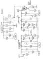
- a microcomputer chip 10 which employs features according to one embodiment of the invention.
- the chip 10 is a semiconductor integrated circuit of the MOS/LSI type including a silicon bar of less than about 200 mils on a side, mounted in a standard 40-pin package.
- a digital processor having a ROM or read-only memory 11 for program storage and a RAM or read/write memory 12 for data storage, along with a CPU 13.
- the CPU consists of an arithmetic logic unit or ALU 14 with its working registers 15 and busses 16, along with a control ROM or CROM 17 for generating microinstructions or control signals on lines 18.
- the CPU 13 accesses the ROM and RAM memory 11, 12 by three busses: a memory data bus MD, a high address bus AH, and a low address bus AL, along with three of the control lines 18. Communication with devices external to the chip is by means of four 8-bit ports A, B, C and D which are accessed by the MD bus and operated by peripheral control circuitry as will be described.
- the MD, AH and AL busses are each eight bits wide, as are the ALU 14, the registers 15 and the ports, although of course concepts herein described would be applicable to 4-bit, 16-bit or 32-bit devices, for example.
- the registers 15 in the CPU 13 include an instruction register IR, a status register ST, circuitry BCD for binary-coded-decimal constants, a shift circuit S which receives the output of the ALU 14, a register T/MAH which functions as both a temporary store for operands and for the high order byte of the memory address (memory address high), a sixteen bit program counter split into two eight bit registers PCH and PCL (program counter high and low); a stack pointer SP, and a memory address low register MAL.
- Address buffers 19 generate true and complement address signals on busses AH' and AL' from the address busses AH and AL. Operands are for the most part stored in the RAM 12 which functions as a register file RF, rather than in temporary registers 15 associated with the CPU 13.
- the busses 16 interconnect the various registers 15, the ALU 14 and MD, AH' and AL' busses.
- the ALU 14 always receives a P input from a P bus and an N input from an N bus, and produces an output via shifter S to an output or O bus. Access to these P, N and O busses 16, to the registers 15 and ALU 14, and to the MD, AH and AL busses is controlled by the control signals 18 from the CROM 17.
- the microcomputer chip 10 operates on the basis of 8-bit macroinstruction words stored in the ROM 11 and transferred to the instruction register IR one at a time.
- One example of a macroinstruction set executed in the CPU 13 is described in Table A which will be discussed in detail below.
- the Table gives the instruction word in mneumonics, also referred to as assembly language or source code, and also gives the machine-language opcode in binary (this is like object code except object is in hex). Usually an opcode plus one or more address bytes are used to execute an instruction.
- An instruction word or opcode held in IR is an input to an entry point circuit 21 which produces an 8-bit address via lines 21 a to address circuitry 22 for the CROM 17, accessing one of 256 possible CROM addresses (in the example embodiment) to produce signals 18 defining a microinstruction as set forth in Tables B and C, to be described below.
- One macroinstruction of Table A produces a sequence of microinstructions. A part of each of the microinstructions (i.e. some of outputs 18) is used to generate the next CROM address; a microjump address is fed back to the entry point circuit via lines 23, and dispatch control information is fed back via lines 24, as will be explained.
- a sequence of microinstructions is generated from each macroinstruction in IR, also dependent upon status bits in the status register ST and other conditions. Addresses for operands, if needed, are contained in words from ROM 11 following the opcode and are transferred to MAL or MAH while the opcode stays in IR during this sequence.
- a map of the logical address space for the microcomputer of Figure 1 is shown in Figure 2.
- the example embodiment employs 8-bit AH and AL addresses, providing a 16-bit address, and so 2 16 or 65,536 bytes are available in this space (often referred to as "64K" bytes where one "K” is 1,024).
- the addresses are shown in four hexidecimal digits, ranging from the first address 0000 to the last FFFF. In this description memory addresses will be given in hex, unless noted.
- a page is 2 8 or 256 bytes, i.e. all addresses on a page are defined by AL and the page is selected to AH.
- the microcomputer 10 uses the zero page (addresses 0000 to OOFF) for the register file RF in RAM 12, the "one" page (addresses 0100 to 01 FF) for the peripheral file PF, and the FO to FF pages (addresses FOOO to FFFF) for the program memory of ROM 11. Some of these spaces for RF and ROM 11 may not be populated, depending upon the size of the ROM and RAM chosen. Other space such as 0200 to EFFF is available for the expansion modes as will be explained.
- the control circuitry responsive to the AH' and AL' busses and control bits 18 defines the way in which the CPU 13 accesses the peripheral file PF including external ports, timer, reset and interrupts, as well as memory control.
- An I/O and interrupt control register 25 at memory location 0100 of Figure 2 is loaded directly by the MD bus and is part of the ALU/register strip; this register contains two memory mode control bits which define the memory expansion modes as will be described, as well as interrupt masks and flags.
- a programmable timer and event counter is also included in this peripheral control circuitry, and comprises a counter 26, a register 26a which functions as start/stop control, input select and prescaler, a control 26b, and a capture latch 26c.
- the counter 26 is a fixed divide-by-8 pseudorandom 8-bit shift counter which simply divides its input by eight.
- the input to the counter 26, which may be an internal clock or an external clock or event, goes through the prescaler part of the register 26a which is an additional 5-bit divide-by-N counter loaded (via a prescale register) from the MD bus with any number up to thirty-two.
- the 8-bit timer register 26g is loaded from MD with the desired final count, up to eight bits or 256. When this count is reached, an interrupt INT2 is signalled.
- the instantaneous count may be read out on MD via the 8-bit capture latch 26c without stopping an ongoing count in the counter 26; this is instigated by INT3.
- a group decode circuit 27 and memory control circuit 28 receive the AH' and AL' address bits and three control signals 18 (#MEM, #WR and #MEMCNT) and produce controls which select between the ROM 11, RAM 12, ports A, B, C or D, the timer or I/O control, etc. for access by a given address. Only one of these is activated in any one cycle.
- the group decode 27 and memory control circuitry 28 likewise generate commands for controlling and/or selecting functions as will be explained.
- interrupt input pins INT1 and INT3 are provided, in addition to the timer interrupt INT2. These inputs are connected to interrupt control circuitry 29 which is also responsive to the contents of the register 25.
- a reset input RST is used to zero or initialize the microcomputer, overriding any function or interrupt.
- a mode control input pin MC connected as an input to the peripheral control circuitry provides a selection of the operating modes (along with the internally-loaded bit-7 and bit-6 of the I/O control register 25).
- Figures 2a to 2e are memory maps showing the unique parts of the address space for these modes; the register file address space RF remains the same as Figure 2 for all modes.
- the modes are: (1) single-chip microcomputer mode where all memory is on-chip in the ROM 11 and RAM 12 as in Figure 2 and the peripheral file PF is configured as in Figure 2a, this being the primary mode of operation; (2) a peripheral expansion mode of Figure 2b where some additional off-chip circuitry may be accessed in the PF space via ports B and C; (3) a full expansion mode of Figure 2c where almost 64K bytes of off-chip memory may be accessed by ports B and C, the RF and ROM being the same as Figure 2; (4) a microprocessor mode of Figure 2d where the on-chip ROM 11 is ignored and all program memory is off-chip, but the on-chip RAM 12 is used as Figure 2; or (5) the emulator mode of Figure 2e in which both the peripheral file PF and the on-chip ROM 11 are disabled and all I/O and program memory is off chip, accessed by ports B and C with the on-chip RAM 12 or RF being used as in Figure 2.
- Input/output buffers 30 connect the ports A, B, C, D to the MD bus, as defined by direction control registers P7, P9, P11, for some modes and by the mode control arrangement via group decode 27 and memory control circuitry 28.
- the RAM 12 is of the dynamic type using one-transistor cells with transparent refresh.
- On-chip RAM for microcomputers is usually of the static or pseudo-static type; if the RAM is of the dynamic type as in Patent 4,074,351, then the refresh function may interfere with access by the CPU.
- the microcomputer of Figure 1 contains a refresh address counter 31 which is self-incrementing and may produce a new 5-bit row address to the row address decoder 12X every machine cycle, so one row of the RAM is accessed for refresh if none is accessed by the CPU. If a memory 12 access cycle is occurring, however, the counter 31 is not incremented and the refresh address output of the counter 31 is not applied to the decoder 12X.
- the RAM 12 is of the folded-bit-line type with a memory bit and its complement on opposite sides of sense amplifiers 12S; i.e., dual memory bits are employed instead of dummy cells traditionally used in dynamic RAMs.
- 128 byte RAM of the example 128x8 or 1024 bits are needed, and with two one-transistor cells per bit the RAM array 12 has 2048 one-transistor cells.
- the array is partitioned 32x8x4, so the X decoder 12X is a one-of-32 select, the Y decoder 12Y is a one-of-4 select for each of the eight input/output bits of the RAM, and thirty-two sense amplifiers 12S are used.
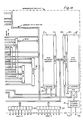
- the microcomputer of Figure 1 is illustrated in chip layout form.
- a major part of the area of the chip 10 is occupied by the memory including the ROM 11 and RAM 12 with their address decoders.
- the ROM 11 has associated with it an X address decoder 11X and a Y address decode and ROM data output circuit 11y of conventional design; eleven address bits are used to define one of 2048 eight-bit bytes in the ROM (twelve bits if a 4096 byte ROM is employed), so an address for the ROM needs both the MAL and MAH registers, i.e., address bits from both AL and AH busses.
- the RAM has an X address decoder 12X which selects 1-of-32 row lines, and a Y address decoder 12Y which selects 1-of-4 column lines, so only seven bits are needed for the RAM select (eight if a 256 byte RAM is used).
- Another major part of the chip area is the control ROM 17 and its associated X and Y decoders 22X and 22Y, and output buffers 17b. If fully populated, the number of bits in the control ROM would be 256 times the number of output lines 18. Only forty-five output lines 18 are needed for the example instruction set of Table A, and only 160 microinstruction addresses as in Tables B and C, so the control ROM is only 160x45 or 7,200 bits.
- the output ports A, B, C, and D each have eight bonding pads on the chip (total of thirty-two) for connection to external, and the areas of the chip around these bonding pads are occupied by the buffers 30 used for the ports. It will be noted that the port A is only used for input, so the space needed for the input buffers for this port is much less than for the remaining ports B, C, and D which require tri-state output buffers.
- the "strip" which is an array of rows (parallel to control lines 18) and columns (parallel with metal bus lines 16 and register/ALU bits 14,15) containing all of the 8-bit registers, ALU bits, and like circuitry associated with the busses 16 and control lines 18.
- ALU 14 and its associated registers IR, ST, S, T/MAH, PCH, PCL, SP, and MAL us described above are laid out on the MOS/LSI chip 10 in a regular strip pattern as seen in Figure 3.
- circuitry connected to the busses and having controls 18 shared by eight bits is also in the strip, such as entry point 21, address buffers 19, timer 26, I/O control register 25, etc.
- Each of these registers as well as the ALU contains eight bits or stages which are laid out in a pattern like memory cells, the bits arranged horizontally and aligned vertically as seen in Figure 3.
- the MD, AL, AH, O, N and P busses of Figure 1 are each eight parallel metal strips on top of the cells of the ALU and registers (rather than beside the registers as depicted in Figure 1), and all of the dozens of control lines 18 are horizontal polysilicon lines typically used as the control gates for transistors in the ALU 14 and its registers and like circuitry.
- the number of control lines 18 needed for the ALU 14 is greater than for a single register such as the MAL register, for example, and conveniently the space needed to lay out the ALU stages is greater than for a single register, so waste space in minimized. That is, the space needed in the control ROM 17 to generate the controls 18 is about the same as the space needed for the controlled circuitry.
- This layout arrangement is indeed advantageous because the ALU and registers fit alongside the control ROM with virtually none of the wasted space used merely for routing conductors in conventional construction of microprocessors. All bus lines MD, AL, AH, O, N and P, and all control lines 18 are routed over functional regions or cells of the chip rather than over unused silicon, and almost all 90 degree turns are produced inherently at functional cells rather than in conductor routing.
- FIG. 3a shows a small part of the strip, two-bits wide, illustrating the metal bus lines and the polysilicon control lines 18 for an N-channel silicon gate MOS device made generally by a single-level polysilicon process according to U.S. Patent 4,055,444, assigned to Texas Instruments.
- Various contacts would be made within each register bit or stage from metal to silicon or to polysilicon.
- the placement of the registers 15 is such that the N bus need not co-exist in any register with the AL or AH busses, and the P bus ends where the AL bus starts, as illustrated in Figures 1 and 3a.
- Some of the clocks needed in the registers and ALU of the strip are run in metal lines like the busses 15 (H1 shown in Figure 3a) so these place further constraints on the density and make the strip concept and bus/register optimum placement more significant.
- Connections from MD to P or N busses are made by transistors located in the strip like a register and labelled MDtP, MDtN; since this logic requires eight parallel bits of transfer gates, tied to sets of eight parallel busses, and using CROM outputs 18 as controls, it fits well in the strip.
- the CROM 17 fits alongside the strip to provide the controls 18 in the control-intensive areas of the ALU and register/bus connections, and alongside the entry point circuitry 21 where the address control and jump address lines 23, 24 are needed.
- the design is oriented toward the control ROM as the source of all controls rather than random logic, and the chip layout of Figures 3 and 3a illustrates that the area of the chip is dominated by the ROM, RAM and CROM with their decoders, and the strip containing a regular array of ALU/register bits, with little space occupied by other control logic.
- This design approach is enhanced by and enhances the microprogramming facility which makes the microcomputer 10 particularly easy to modify by changing the micro or macrocode.
- the microcomputer 10 may be modified at three levels, plus the mode control.
- the first level is changing the ROM code of the ROM 11, and of course this is the most widely practiced modification.
- the ROM code is defined by a single mask in the manufacturing process as set forth for example in U.S. Patents 3,541,543, 4,208,726 or 4,230,504, assigned to Texas Instruments.
- the macroinstruction set may be supplemented (keeping basically the same microinstruction set), or the microinstruction set may be changed, both of these levels requiring changes in the CROM 17 code upon manufacture.
- the CROM code is defined by a single mask in manufacture, just as the ROM code, so physically it is just as easy to change the microinstruction set; however, the macro assemblers and micro assemblers (computer programs used as design aids for customers) then are different.
- the sizes of the ROM and RAM may be increased to allow more complex algorithms to be programmed in the ROM code, and the size of the CROM 17 may be increased to provide more complex micro- and/or macro-instruction sets. It is important to note that the mode control MC (and bits 6-7 of register 25) allows changes without any type of physical or mask change; no fuse links or the like are needed.
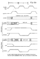
- the microcomputer chip 10 operates from a basic clock frequency referred to as Xtal in Figure 4. This frequency of about 5 MHz is supplied by an internal oscillator 33 controlled by an external crystal coupled to two pads labelled Xtal in Figure 1 or 3. From the clock Xtal, clock generator circuitry 33 produces four basic overlapping half-cycle clocks H1, H2, H3 and H4 for each microinstruction cycle or state time S1, S2, etc., as seen in Figure 4. Each state time equals two complete cycles of the clock Xtal. H4 overlaps two state times.
- Short memory cycles to access the RAM 12 are completed in one state time such as S1 of Figure 4; #MEMCNT is low and all bits of the AH bus are low during H1, and the RAM address is valid on the AL bus while #MEM is high.
- the write control #WR is high for write or low for read.
- the data accessed is then valid on the MD bus during H4 at the end of the cycle, extending over into the beginning of the next cycle, so the data may be loaded into the registers T or IR at the end of a cycle or gated onto the P or N busses at the beginning of the next cycle.
- All memory references to the register file RF in the RAM 12 use this short cycle; all other memory references (i.e., to the on-chip ROM 11, the peripheral file PF, and extended memory) require two microinstruction executions and are called long memory cycles as illustrated in Figure 4.
- the memory continue command #MEMCNT is high during the first state time and low during the second.
- the memory command #MEM must be high during H1 of both cycles, and the address valid on AH and AL during H1 of the first cycle.
- the write command #WR is low from the beginning of the first cycle through H1 of the second, and the data is valid during H4 beginning at the end of the second cycle.
- #WR is high, and the write data is gated onto the MD bus for H4 of both first and second cycles.
- the address on the AH' and AL' busses becomes valid during H2. This address is based on the address loaded onto AH and AL during H1.
- the array is precharged during H1 with all row or X lines going to Vss and all column or Y lines going to Vcc, then the ROM X address gated into the array from decoder 11X beginning at H3 and the ROM Y address coming valid at the beginning of H4, so the ROM output is valid at H4.
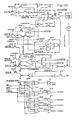
- the CPU 13 in the microcomputer 10 of Figure 1 consists of the ALU 14, the registers 15 and the busses 16 controlled by the CROM 17.
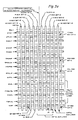
- Figure 5 a more detailed block diagram of the ALU and shifter S and the associated busses is shown, and Figure 6 shows the CROM 17 and its microinstruction output bits 18. Control of the ALU and access to the busses is defined entirely by these microinstructions or bits 18, identified in Figure 6 for the illustrative embodiment.
- An 8-bit address on lines 21a from the entry point circuitry 21 contains a 6-bit X address on lines 21X and a 2-bit Y address on lines 21Y.
- the lines 21X are connected to X decoder 22X which selects one of up to 64 X lines in the array of ROM bits of the CROM 17.
- the lines 21Y are connected to a Y decoder 22Y which selects 1-of-4 in each group of four Y lines (only forty-five groups used).
- a different "microinstruction" is output on the lines 18; a microinstruction may have any number of the lines 18 active, but usually a combination of only a few lines 18 is active for a given microinstruction.
- Each line 18 goes to a buffer 17b to drive a higher capacitance load than the array output Y line itself would allow, and to clocked gates and other such logic as needed. All microinstruction bits (control lines 18) in Figure 6 and throughout this description are referred to with a prefix "#".
- bits are active low and thus have a minus sign prefix, like #-OtST.
- #-OtST means "0 bus to ST register", i.e., the gates connecting the 0 bus to the status register are activated by this bit.
- the eight bit jump address on the lines 23 is denoted #JmpAddr (7-0), while the 3-bit jump control on the lines 24 used for dispatch addressing is denoted #JmpCntl (2-0); these eleven bits are used in the entry circuit 21 to generate the next CROM address. All of the twenty-one bits 18 from #OtPCH down to #ONEtAH in Figure 6 control the access to registers 15 from busses 16.
- #LowWriteO and #LowWrite1 are decoded to produce pseudo-microinstructions OtPCL, OtMAL and OtSP.
- the bits #ONEtAL and #ONEtAH place a "1" on the AL or AH busses to generate the B register address 0001 or the PF page address 0100 (hex) in a microinstruction.
- Default to all 0's on AL and AH is A register address in the register file. Connections between registers 15 and busses 16 are described in detail below.
- the #MEMCNT bit is a "memory continue" control for long memory cycles; the RAM 12 can be accessed for read or write in one state time, but the ROM 11 or peripherals in PF require two states, so for this reason control line #MEMCNT is active in the first state of every long memory cycle as seen in Figure 4.
- #MEMCNT is used to form several other control signals, and always identifies the first or second state of a long memory cycle.
- the #MEM bit signifies a memory cycle and is active whenever ROM 11, RAM 12 or external memory is accessed.
- the #WR bit is a write command, so if #MEM and #WR are active a memory write condition exists, while if #MEM is active and #WR is not, a memory read condition exists.
- the #-LST signal is a load status command for ALU operations; the status register ST can also be loaded from the 0 bus by the #-LST command.
- the ALU is controlled by nine bits labelled #ShiftCntl (3-0), #AluCntl (3-0) and #ABL; these controls will be described below in detail.
- microinstruction bits 18 are physically arranged in the order used in Figure 7a-7e rather than in the order shown in Figure 6, so that a control bit 18 is generated as close as possible to the point it is used in the strip.
- the P bus is one of the inputs to the ALU 14. It is called 'P' for "Positive", because in a subtract operation where the ALU 14 only computes P N the P bus contains the positive, or left-hand, operand.
- the P bus is loaded from the MD bus via transistors 16a, 16b, and 16c, loaded from the AL bus via transistor 16d ( Figure 7b), loaded from the PCH register via transistor 16e, or from the PCL register via transistor 16f. Any of the AL bus sources may be placed on the P bus by gating them on the AL bus and asserting the #PAL microinstruction bit going to the gate of transistor 16d, connecting the P bus to the AL bus.
- the P bus assumes the value of all zeros.
- the P bus is loaded in the beginning of a microinstruction cycle, on phase H1. All of the possible P bus sources and the microinstruction bits or outputs 18 needed for each are as follows:
- the N bus is the other input to the ALU 14. It is called N for "negative", since on the ALU subtract operation it contains the negative, or right-hand, operand. It is loaded from the MD bus via transistors 16a, 16g and 16h, loaded from the T/MAH register via transistor 16i, loaded from the IR register via transistor 16j, the status register ST via transistor 16k, or the BCD constant register via transistor 16m. It is understood, of course, that there are sets of eight of each of the transistors 16a to 16j, one for each of the eight bits of each bus and each register. Only four transistors in the sets 16k or 16m are needed.
- the source of the N bus is indicated directly by a bit in the microinstruction word, as shown below. If the bit is '1', the source is gated onto the N bus. If no source is specified, the N bus assumes the value of all zeros. The N bus is also loaded at the beginning of a microinstruction cycle, on phase H1.
- the AL or address low bus holds the lower eight bits of all memory addresses. This comprises the entire address for references to the register file RF in RAM 12, or the lower byte for references to the peripheral file PF, on-chip ROM 11 and extended memory in expansion modes.
- the AL bus is loaded during the- phase H1.
- the sources of the AL bus are the MAL register via transistor 16n, the SP register via transistor 16p, or the constant 01 via transistor 16q.
- the constant is provided to efficiently address RAM location 01 which is the "B" register. If no source is specified, "default", the AL bus assumes the value 00 which is the A register in the RAM.
- the AL bus may also be connected to the P bus via transistor 16d by asserting the #PAL microinstruction bit.
- the AL bus sources MAL, SP, and the constant 01
- the P bus sources PCH, PCL, and MD bus contents
- the MD bus contents moved in this case are those present at the start of the microinstruction.
- the 8-bit AH (Address High) bus contains the high-order byte of the address referenced by the CPU, loaded during H1. It may be loaded with the contents of the PCH register via transistor 16r, the T/MAH register via transistor 16s, or the constant 01 via transistor 16t.
- the high byte of the program counter is usually transferred to the buffers 19 for use in the peripheral control circuitry 20, and the T/MAH register is used to hold the high byte of other addresses in memory for use in a later microinstruction state.
- the constant 01 is provided to efficiently access addresses in the peripheral file in this embodiment (i.e. page-one addresses of the form 01xx in hex). If no source is explicitly specified in the microinstruction word, "default", the AH bus takes on the value 00; this is useful for referencing the on-chip register file RF in RAM 12.
- the sources of the AH bus are summarized below:
- the O or output bus always contains the output of the ALU 14 and shifter S combination.
- the O bus contents may be loaded onto the MD bus via transistors 16u and OtM, or into the PCH, PCL, MAL, or SP registers via sets of eight each of transistors 15a to 15d, respectively.
- the status register ST is loaded from O bus by the true-low microinstruction bit #-OtST and four transistors 15e ( Figure 7e).
- the PCH register is loaded by the true-high microinstruction bit #OtPCH.
- the load signals for the other destination registers (MAL, PCL, SP) are encoded in the two microinstruction bits #LowWrite(1-0), according to the combinations of #LowWrite(1-0) below:
- the 0 bus may be gated onto the MD bus via transistors 16u by specifying the appropriate values of the #MEMCNT and #WR microinstruction bits so that OtM will be asserted by the peripheral control circuitry 20.
- the O bus contents may then be loaded into the T/MAH or IR register from the MD bus via transistors 15f and 15g.
- the O bus is loaded during phase H4 of the microinstruction cycle. It contains the result of the ALU and shifters operations specified in the current microinstruction.
- the memory data bus MD is a bidirectional bus that transfers data to and from the CPU 13. Data is valid on MD during phase H4 of the microinstruction cycle, which spans two microinstructions. For example, data may be read via transistors 16b from the MD bus onto the P bus at the beginning of a cycle H1 and the ALU results then loaded back onto MD via transistors 16u at the end of the cycle at H4.
- the MD bus contents may be loaded on the P or N busses via transistors 16c or 16h, as described earlier ( Figures 5 or 7b).
- the results of the previous microinstruction (or the data read from memory by it), may be loaded into the ALU 14.
- the MD bus may be loaded in one of three ways;
- the MD bus contents are controlled by the peripheral control circuitry which sends the OtM signal to the CPU to signal loading the bus from the 0 bus.
- the CPU 13 requests use of the MD bus by asserting combinations of the #MEM, #MEMCNT, and #WR signals, as outlined above.
- the group decode and memory control 27, 28 in the peripheral control circuitry 20 sends signals to the on-chip ROM 11 and RAM 12 to control their accesses to the MD bus.
- the data on MD bus is available at the end of the same microinstruction cycle that initiated the read.
- Data on MD may be loaded into the T/MAH or IR registers during that microinstruction by specifying the #MDtT or #-MDtIR bits, respectively, or may be loaded into the P or N bus on the next microinstruction by specifying the #MDtP or #MDtN bits in the next microinstruction.
- the O bus data is placed on the MD bus, and the #WR control asserted.
- the desired address is placed on the AH and AL lines, and the #MEMCNT command asserted in the first of the two cycles required.
- the data is available on the MD bus.
- LDADDR Low Density Memory
- the memory address is latched in buffers 19 going to AL' and AH' and the peripheral control circuitry 20 on the first cycle, and need not be asserted on the second cycle.
- the address is specified in the first cycle, and the data is placed on the MD bus for the first and second cycles.
- the MD, P, N, AH, AL and O busses are precharged on H2 or H3 by transistor 16v as indicated.
- the arithmetic logic units or ALU 14 as seen in block form in Figure 5 and in detail in Figures 7c and 7c' accepts as inputs the values on the P bus via transistors 14a and N bus via transistors 14b.
- the ALU outputs its result to the shifter S during H4 via line 14c and transistor 14d. Its operation is controlled by the #AIuCntl(3-0) bits inputted via buffers 17b and transistors 14e, and by the #ABL bit going to transistors 14f, both from the current microinstruction.
- the ALU operates on the values loaded on the P and N busses during H1 of the current microinstruction, and produces an 8-bit ALU output on lines 14c which is input to the shifter S, and also produces two carry bits: Cout on line 14g, an arithmetic full byte carry bit, and Dout on line 14h, a 4th-bit half-carry bit used by the decimal adjust circuitry in the BCD constant register for binary coded decimal operations.
- the available operations of the ALU controlled by transistors 14e and 14f are defined below:
- the carry-in bit Cin on line 14i of the ALU 14 is specified by the #ShiftCntl(3-0) bits 18 of the microinstruction.
- #ShiftCntl(3,2) bits are zero and the possible carry-in bits are defined in logic 14j of Figure 7c' as follows:
- the micro carry bit uC is the carry out Cout on line 14g from the ALU operation of the immediately preceding microinstruction. This is not the same as the shift-out bit Sout on line 14k from the shifter S operation of the previous microinstruction.
- the status carry bit STC is the carry bit of the status register ST.
- each ALU bit produces a "generate" on line 14m and/or a “propagate” on line 14n.
- the arithmetic carry-out Cout bit from the ALU 14 on line 14g is generated and/or propagated by transistors 14f, 14p and 14q, depending upon #ABL, and if '1' is there is a carry-out during an add or subtract operation in the ALU.
- For all other operations i.e.
- Cout on line 14g is equal to 0.
- Cout is sent via line 14g to the status register ST circuitry for possible loading into STC, the status carry bit.
- the decimal half-carry Dout is sent via line 14h to the BCD constant register for use in generating a constant for decimal arithmetic correction.
- the propagate bit on line 14n and a carry-dependent bit 14p' are inputs to an exclusive-or circuit 14r, which produces the output 14c.
- an add operation with zero carry in (#AluCntl and #ShiftCntl all zeros) will cause the ALU to calculate the sum of the P and N bus contents.
- a '1' must be carried in for this subtract since no borrow was desired.
- the following two microinstructions read the current byte addressed by the PCL and PCH registers, place it in the T/MAH register, and increment the PCL and PCH registers:
- the shifter S of Figures 5 and 7 performs a variety of 1-bit shift operations on the outputs 14c of the ALU 14.
- the #ShiftCntl(3-0) bits on control lines 18 to the ALU control the following entities:
- the shift-out bit Sout on line 14k shifted out in a rotate instruction is sent to the status register ST. It will be loaded in ST as the new status carry bit STC if the #-LST microinstruction bit is set.
- the 8-bit instruction register IR is a register intended to hold the current machine opcode (one of the opcodes or first bytes of the Table A instructions).
- the opcode is loaded through transistors 15g from the MD bus by the #-MDtIR bit in a microinstruction.
- IR may be loaded onto the N bus with the #IRtN bit through transistors 16j.
- the output of IR includes true outputs IRO to IR7 and complement outputs -IRO to -IR7, all on lines 21b; this output primarily is used in the entry point circuit 21 as will be described.
- Each of the bits of the register 15 of Figure 7 basically consists of two inverters 15i with the output coupled back to the input via a transistor 15j. All transistors 15j are clocked on H2 except for IR and ST in which the transistor is clocked on H1.
- the status register ST of Figures 5 or 7e is a 4-bit register indicating various conditions of the machine. Each bit of the status register has a special meaning, and has separate circuitry devoted to it. Only bits 4-7 of ST are used in this example, but other embodiments could use additional bits.
- STC or the "C" bit referred to in instructions of Table A is the status carry bit. It holds either the carry-out of the ALU 14 from line 14g, the shift-out of the shifter S from line 14k, or the decimal arithmetic carry-out from line 14h.
- STSB is the status sign bit ("N" in Table A), and contains the most significant bit of the O bus contents.
- STEZ is the status equal to zero bit, and contains a '1' when all bits of the O bus are zero which is detected by transistors Sz and line Sz2 in shifter S.
- STINT is the status interrupt enable bit. Bits 3-0 of the status register are not used in this embodiment but may be used in expanded versions of the device; the value of these bits wherein the ST register is loaded onto the N bus is undefined.
- the status register bits may be modified in one of two ways:
- the input to the status equal to zero STEZ bit is the micro equal-to-zero bit, uEZ from the shifter S, derived from the transistors Sz.
- the uEZ bit is simply the logical NOR of all O bus lines. That is, if all O bus line are zero, the uEZ is set to '1'. Otherwise, it is set to '0'.
- the status interrupt enable STINT bit may only be modified by loading the 0 bus contents into the status register ST via transistor 15e when #OtST is asserted.
- the STINT bit corresponds to bit-4 of the O bus in this case.
- All of the status bits may be loaded from the status register ST to the N bus via transistors 16k.
- the STEZ, STSB and STC bits go to the entry point circuit 21 via lines 21b.
- the micro architecture of the invention including entry point circuit 21 and CROM 17 is designed to dispatch on various subfields of the IR contents, providing for the execution of appropriate microcode as in Figure 8 and Table B and C for each machine opcode or Table A instruction.
- Figure 9 shows a map of the opcodes.
- the opcode in IR may be considered to have two possible formats, and the entry point circuit 21 seen in detail in Figure 10 responds to these formats to produce the address on lines 21a:
- group and “function” refer to logical subsets of machine opcodes.
- the group field in an opcode indicates the addressing mode of the instruction (i.e. which group of Figures 8b to 8d to go to on the first dispatch at decision point 8m), and the function field indicates the arithmetic or logical operation performed on the operands on the second dispatch at points 8n of Figures 8b to 8d, after the operands are fetched.
- the microarchitecture allows significant sharing of microinstructions among opcodes within the same group or function.
- microcode state RFtoA-1 which fetches the A register and a general RF register, as seen in Figure 8 and as will be explained in reference to Tables B and C.
- Dispatching on an IR subfield may be performed on one of the first microinstructions after the IR is loaded (e.g., at IAQ-2). Thereafter, dispatching may be performed by microinstructions up to and including the next one that reloads the IR. If no dispatching is required during executing a given opcode, then the IR may be used as a general purpose 8-bit register.
- the flow of control between microinstructions is determined by how the next microinstruction address on lines 21a to CROM 17 is generated in the circuit of Figure 10, in both conditional and unconditional branching.
- the dispatching capability of the processor is used to share microinstructions among several macroinstructions.
- microinstructions of Tables B and C stored in the control ROM or CROM 17 on the chip, may be characterized as horizontally microprogrammed in that each microinstruction indicates the address at which the next microinstruction to be executed is located.
- the next micro-address is specified by two fields of the CROM output 18 (lines 23 and 24) indicated as inputs in the logic circuit of Figure 10;
- microinstructions In the example device, a maximum of 256 microinstructions are possible, each consisting of a multi-bit word (outputs 18) in Figure 6, but a total of only 160 microinstructions are required to implement the Table A instruction set, and so only 160 words of CROM are formed. Each of these is only a 45-bit word, containing a possible forty-five outputs 18 of microinstruction control. Additional microcoded functions for the device (new macroinstructions not in Table A) may be added by implementing a subset of the Table A instruction set, or replacing it entirely. The functions executed may be expanded by using a larger CROM 17, requiring more bits in the address 21a, and for more bits 18 for the output, in other embodiments.
- the dispatch field bits (like bit-3 to bit-0 in Figure 8k) actually replace the low order address bits in the #JmpAddr(7-0) field; they are not ORed with them. For example, suppose #JmpAddr was specified to be 00010001, and the #JmpCntl(2-0) lines set to '110', indicating a dispatch on STC, the status carry bit input to logic circuitry 21m. If STC were '0' the next micro address would be 00010000.
- the possible dispatch fields implemented in Figure 10 are summarized in Table E, and each of the dispatch possibilities is further explained below; however, the microinstruction sequences for the illustrative instruction set will be examined.
- Figures 8a to 8j a flow chart of the microinstructions of Tables Band C as executed to implement the macroinstruction set of Table A is illustrated.
- Figures 8a to 8j reference the microinstructions of Table C by name, as well as the CROM addresses of Table C in hex.
- Table C is only a partical listing of the microinstruction set. Execution of each of the Table A macroinstructions begins with the instruction acquisition IAQ sequence of Figure 8a, starting at IAQ-0. Assuming no interrupt or reset is asserted, a group dispatch is performed on the group field at IAQ-2, selecting one of twenty-four addresses for one of the operand addressing modes or for miscellaneous jumps or traps.
- the address is formed by the CROM bits in the #JmpAddr (7-0) field of the current microinstruction. This type is used for sequences like BtoPPL-0, BtoPPL-1, BtoPPL-2, etc. of Figure 8b.
- the next type is function dispatch used to select the function at decision points 8n, SOPFUNN, DOPFUN, etc. in Figures 8a-8d.
- Function dispatch is defined in Table F.
- the base address for dispatch is formed in the #JmpAddr(7-0) field of the microinstruction.
- the next micro address is determined by replacing the bits 3-0 of the base address with bits 3-0 of the IR register, so the offset can be up to sixteen. To avoid confusion, the base address should be a multiple of sixteen (i.e. the lowest four bits of the base address equal '0').
- a function dispatch is a dispatch on the "function" field of the instruction word in the register IR.
- the function field indicates the arithmetic operation to be performed. This is contrasted with the 'group' field, bits 7-4, which indicate the addressing mode of the macro instruction (Table A instruction).
- format "1" instructions have a 3-bit function field (IR bits 2-1-0)
- the function dispatch still performs a 16-way branch on the lower four bits of the IR register.
- the function dispatch for format "1" opcodes thus depends on the value of the IR(3) bit.
- test sign bits dispatch An example is the RJmp-3 microstate of Figure 8d, decision point 8p.
- One is the 8-bit address of the microinstruction to be executed if T(7) is '1', and the other is the address of the microinstruction to be executed if T(7) is '0'.
- the next type of dispatch is "test if zero".
- the entry point logic 21 replaces #JmpAddr(0) bit with a bit which is '1' when the O bus is all zeros and '0' otherwise.
- Another type of dispatch is "test if interrupt”.
- the IACT line is asserted by the peripheral control circuitry 20 when an interrupt condition is detected. IACT can be asserted only when STINT (Status Interrupt Enable) is '1'. Interrupts may be signalled from the external interrupts -INT1 and -INT3 or the internal timer interrupt, INT2.
- Group dispatch Another type of dispatch is "group dispatch”. This is done at IAQ2, decision point 8m of Figure 8a as well as after RFtoA-1 in Figures 8b and 8c at decision points 8q. Note that another group dispatch is possible because the opcode is still in IR.
- the group dispatch performs a 24-way dispatch on the group field by replacing the low order bits of #JmpAddr lines 23 with a function of the group number.
- the high nibble of the IR register, IR(7-4) is placed in the low nibble of the next address, shifted by one bit.
- the low order bit of the next address is IR(3) OR NOT IR(7).
- IR(7) '1'
- the 0 bit of the next address always equal '1'.
- the machine will jump to a micro address which is the base address plus (group * 2) +1 for format '0' group numbers.
- the machine will jump to a micro address +IR(3) for format '1' group numbers.
- the CROM addresses "base address”, “base address+2", “base address+4", etc. may be used for other microinstructions; only alternate CROM addresses are used after the 24-way group dispatch.
- the example microinstruction set of Tables B and C and Figure 8 uses the group dispatch at IAQ-2 after the instruction is loaded into the IR. Each "group” corresponds to one of the addressing modes, and the microcode executed after the dispatch fetches the appropriate operands for this instruction. A "function" dispatch is then done, and the microcode branches to perform the appropriate ALU operation on the operands. In this manner, the operand fetch microinstructions are shared among the instructions, but each instruction has its own microcode to perform the function of the instruction.
- a "test if carry" type of dispatch is also available.
- test status register or macro jump.
- This dispatch tests eight possible conditions of the status register, indicated by the three bits in IR(2-0). If the condition is true, control transfers to the base address plus 1. If the condition is not true, control transfers to the base address.
- the conditions tested for macro jump are indicated in Table 1.
- the base address field must be even and is placed into the #JmpAddr field of the microinstruction.
- the result of the condition test is placed in bit 0 of #JmpAddr to form the new microinstruction address.
- the macro jump dispatch is used in the microcode of Table B and Figure 8 to implement the conditional branch instruction at RJmp-3, selecting Rjmp-4 or -5.
- microstate Reset-0 of Figure 8e Another type of dispatch is the reset operation, microstate Reset-0 of Figure 8e.
- the peripheral control circuitry 20 asserts the RST signal to the CPU.
- the entry point logic 21 of Figure 10 immediately forces the next microinstruction address to be hex FF or all ones by transistors 21n, grounding the lines 21a on H1.
- the microcode does not poll the RST line; rather, the microinstruction executed.
- the sequence of microinstructions RESET-0 to RESET-3 of Figure 8a executed upon reset results in fetching a subroutine entry point address at address FFFE in memory (in the on-chip ROM 11) and branching to this subroutine.
- the macroinstructions of Table A are shown also in an instruction map of Figure 9 wherein the most significant half MSH of the instruction is listed across the top and the least significant half LSH is listed down the left side, in binary and hex.
- an ADD instruction with an addressing mode of "B, A” has an opcode of 0101000 in binary or 68 in hex; this addressing mode means that the contents of the B register or R1 in RAM 12 is added to the contents of the A register (RO in the RAM) and the sum is written into the A register, so B is the source address and A is the destination address.
- the B, A addressing mode uses the least possible states in execution, and shares some of these states with several other instructions, such as MOV, AND, OR, XOR, SUB, CMP, etc., all of which have the same MSH opcode of 0110.
- the ADD B,A and MOV B,A instructions are dual operand instructions using the A and B registers.
- the A.or B register (or B,A) addressing modes require only five machine states to execute, three of these being instruction acquisition shared by all.
- Register file addressing is also available for most instructions; this mode is identified by Rn in Figure 9, and means that one of the 128 or 256 registers in the register file RF or RAM 12 is the source or destination address. So, for an instruction "ADD Rn, Rn" the opcode is 00111000 ( Figure 9) followed by two 8-bit addresses of the two resigers Rn, Rn used for the source and destination operands; thus three bytes are needed for an ADD Rn, Rn instruction. To execute such an ADD Rn, Rn instruction, ten machine states are used, but the source and destination fetch states are shared with all other similar instructions such as AND, OR, MOV, SUB, CMP, etc., all having a MSH opcode of 0100.
- Register file addressing with A or B register addressing is used in the MSH columns for 0001 and 0011 opcodes, for all of the common arithmetic and logic instructions.
- single operand Rn addressing is used for instructions of the Rn or 1101 column of Figure 9.
- ADD R113, A means add the contents of A register to the contents of the 113th register in RF or RAM 12 and store the sum in the register R113.
- MOV R5, R78 means copy the contents of R5 into R78.
- DEC R78 means decrement the contents of R78. Since the A and B registers are in the register file as RO and R1, these may be used in the Rn, Rn addressing mode.
- All of the major instructions can use the immediate addressing mode which is specified by "%n” in Figure 9, particularly the 0010, 0101, 0111 and 1010 columns for MSH.
- Immediate addressing uses the contents of a byte following the opcode byte as an operand.
- MOV %98, R123 means replace the contents of register R123 with the hex number 98; this sequence requires three bytes to define, these being "01110010 10011000 01111011” in machine instruction format (object code in binary as actually coded in ROM 11), and the three bytes would be stored in sequential addresses in the ROM 11, accessed in sequence by incrementing the program counter.
- Peripheral file addressing specifies one of the PF addresses or registers PO to P255 (see Figures 2 to 2d) as an 8-bit field following the opcode.
- the I/O ports A, B, C, D, the timer 26 and the 1/O control register 25 may be accessed (depending upon the operating mode), all by the instructions in the three columns 1000, 1001, and 1010 of Figure 9 containing a Pn notation.
- the instruction "MOVP A, P2" means copy the contents of A register into the P2 address (timer data).
- Another addressing mode is register file indirect; the same five instructions, LDA, STA, BR, CMPA and CALL which can use direct can use register file indirect addressing, and these are in the 1001 column of Figure 9.
- This mode is specified by asterisk * followed by the register name.
- the specified register contains the least significant half of a 16-bit address. The most significant half of the address is contained in the next higher register.
- STA * R45 means copy the contents of register A into address hex 43F8 (where R46 contains 43 and R45 contains F8).
- LDA, STA, BR, CMPA and CALL can employ an indexed addressing mode in which the address of the operand is the sum of the contents of B register and a 16-bit direct address n.
- the address n is preceded by @ and following by (B) so STA @ 43F8(B) means copy the contents of the A register into the memory location specified by the contents of B added to the contents of 43F8 (hex).
- the opcodes for all these instructions start with 1010 as seen in Figure 9.
- the primary operating mode of the microcomputer 10 of Figure 1 is the microcomputer mode in which all of the memory is contained within the ROM 11 and RAM 12.
- the device is initialized by RST or reset to be in the microcomputer mode; that is, zeros are placed in the bit-7 and bit-6 of the I/O control register 25. In this mode, only nine bytes of the peripheral file PF are used, the remaining 247 have no function.
- the peripheral register numbers PO, P2, etc., and hex addresses of the peripheral file registers for the microcomputer mode are shown in Figure 2a.
- Port A is used only for input and port B in only an output, while ports C and D are either output or input; thus, registers P9 and P11 define the direction of data in the ports C and D, but no such control registers are needed for ports A and B as they are unconditionally input or output.
- the port A, B, C, D data registers are contained within the buffers 30 and are accessed by the MD bus, using addresses 04, 06, 08 and OA (in hex) on the AL bus and page-one or 00000001 on the AH bus.
- AL addresses 09 and OB access the control registers contained in buffers 30 for ports C and D.
- a "0" in the control register bit sets the port for input and a "1" sets it for output.
- An address applied to AL and AH in the unused areas will produce no meaningful result, so the ROM 11 program is of course written to avoid these addresses.
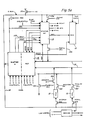
- FIG 10a a system containing an eight digit display 13-1 and a keyboard matrix 31-2 is shown which uses the device of Figure 1 in its microcomputer mode.
- the C port outputs are used for the segments of the display and the B port outputs drive the digits of the display 13-1 and columns of the keyboard matrix 13-2 as illustrated in U.S. Patents 3,988,604, 3,921,142 or 4,158,431 for example.
- the rows of the keyboard matrix 13-2 are applied to the A port inputs.
- Other activators and sensors such as in the microwave oven controller of the Van Bavel patent 4,158,431, assigned to Texas Instruments, may be connected to the D port as inputs or outputs.
- An example of a program for display scan in the system of Figure 13a is available.
- the peripheral page 0100 to 01 FF, 256 bytes is utilized for off-chip accesses.
- the C port is used as a multiplexed 8-bit address/data bus, and four bits of the B bus are dedicated as control lines ALATCH, R/W, ENABLE and Clock Out as illustrated in the system of Figure 13b.
- This system employs the microcomputer 10 of Figure 1 as the main processor in a system which uses two other attached processors.
- One is a video display processor 13f as described in U.S. Patent 4,243,984 issued to Guttag et al, assigned to Texas Instruments.
- the other is a general purpose interface bus adapter chip 13g which allows the chip 10 to interface with a standard IEEE 488 bus 13h.
- the chip 10 produces an 8-bit address on the C port which is latched into an 8-bit latch 13i by the address latch signal ALATCH on port B4, then the address is available on an address bus 13j for the chips 13f and 13g when the enable signal on port B6 goes active.
- the chips 13f and 13g are synchronized with chip 10 by the clock output on port B7.
- the C port is then used for data from or to the chip 10 and chips 13f and 13g, depending upon the read/write control R/W on port B5.
- the chips 13f and 13g are thus configured to respond to addresses 0108,0109 and 010A to 01 FF on busses AL and AH.
- the AH bus of Figure 1 will always contain 01 in this mode for off chip accesses, of course.
- the A port functions as an input and the D port as input or output in this peripheral expansion mode, so other functions are executed aside from Bccessing the chips 13f and 13g; for example, actuators and sensors, or a keyboard matrix as in Figure 10a may be used here also.
- the full expansion mode of Figure 2c and Figure 10c provides the 8-bit address output on C port as in Figure 10b plus another address byte on D port which may address a memory chip 13k, for example.
- the full expansion mode allows a full 64K (two bytes-C port and D port) of off chip address range; addresses 0108 to EFFF are available for off chip access.
- port B at address 0106 provides the memory control and clocking on bits B4, B5, B6, B7.
- the memory chip 13k may be a 32K device, for example, and the lower byte address from C port is latched at 13i while the high byte goes directly to the chip 13k on lines 13m.
- the data bus 13n going to the C port is shared by the chips 13f, 13g and 13k.
- a keyboard matrix 13-2 could be connected to the remaining four bits of the B port (address 0106, bits 0-3) and the A port as shown, however.
- the microprocessor mode of Figure 2d allows the chip 10 of Figure 1 to cooperate as an 8-bit microprocessor; all of the addresses in the range 0108 to FFFF are available for off chip accesses.
- This mode functions the same as the full expansion mode of Figures 2c and 13c except there is no on-chip ROM for program memory; actually the chip contains a ROM 11 but it is not used, so if the ROM code built into the device is not correct then the chip can still be used as a microprocessor in this mode instead of a microcomputer, in which case addresses FOOO to FFFF are treated as external memory locations. The treated as external memory locations.
- the system of Figure 13c may use the chip 10 in the microprocessor mode, in which case the memory chip 13k could be 64K instead of 32K.
- the system emulator mode of Figure 2e facilitates the development of new ROM 11 programs. All on-chip ROM and peripheral file PF is disabled so all addresses 0100 to FFFF access off-chip locations. This mode permits inexpensive development of new systems by allowing the developer to emulate the desired on-chip ROM 11 code, I/O and interrupt structure with temporary external memory chips 13q and logic 13r of Figure 13d.
- the system emulator mode is enabled when the MC pin is tied to a high voltage source (+12v).
- the memory interface operates just like the microprocessor mode of Figures 2d and 10c except for the peripheral file PF and pin out.
- the C and D ports are for addresses and data as in Figure 10c, but the A port is not used (it is emulated off-chip, so the keyboard of Figure 13c, for example, would be connected to the logic 13r).
- Pin B3 is an interrupt acknowledge line, pins B4 to B7 are used as before, and pins BO to B2 are not used (emulated off-chip).
- the CPU 13 in a chip in the emulator mode functions just as if the on-chip ROM and PF is being used, but addresses asserted on the busses AH', AL' result is off-chip access.
- the function of the memory control logic is to control the addressing and timing of all peripherals and all memory expansion modes.
- the memory control circuitry consists of the circuitry contained in the memory control block 28 and the group decode 27 block.
- the group decode circuitry 27 handles all the addressing by: 1) decoding the address lines AH' and AL' to determine which internal peripheral, if any, is being addressed (i.e., the RAM 12, ROM 11, INTERRUPT, TIMER, PORTS A, B, C or D) and 2) determine based on which expansion mode that the processor is currently in, if that peripheral exists internally.
- the group decode 27 outputs of this circuitry identify which peripheral is being addressed.
- Figure 11a illustrates the decoding of the address AH' and AL' and other inputs to group decode 27 as used to specify an internal peripheral.
- the group decoder 27 is a circuit implementation of Figure 11 a.
- the group decode circuitry 27 includes a programmable logic array that interfaces to the address bus AH' and AL' and signals MMDO, MMD1, EM and MP from the interrupt logic circuitry 29 and #MEM from the CPU 13.
- the output of the group decode circuit 27 is the signals which cause the selected one of the internal peripherals to be accessed during a machine state.
- a microinstruction control bit obtained from the microinstruction word signifies a memory operation. Note that in Figure 16a MEM must be low or active for any of the internal peripherals to be accessed.
- EM and MP are derived from the interrupt logic circuitry.
- EM specifies an emulator mode and MP specifies the microprocessor mode.
- MMDO and MMD1 are-memory mode bits (bits 6, 7 of the register 25) which are internally programmable and determine the current memory expansion mode.
- Figure 11b illustrates the five memory expansion modes determined by the external memory configuration pin MC and the two internally programmable memory mode bits MMD1 and MMDO in the control register 25.
- the microprocessor system has the capability to receive two external interrupts INT-1 and INT-3, one internal timer interrupt INT-2 and a reset signal RST.
- the peripheral hardware 20 asserts the IACT signal on a control line to the CPU 13.
- the CPU 13 may then read an interrupt vector supplied by the peripheral control hardware 20 on to the memory data bus MD, indicating which interrupt has occurred.
- the interrupt vector read requires two cycles, as shown in the timing diagram in Figure 4. It should be noted in Figure 4 that both #MEM and #WR must be low during both cycles of the interrupt vector read. Like a long memory read, the vector is not available until the end of the second microinstruction cycle as seen in Figure 4.
- the value of the vector supplied by the peripheral circuitry 20 for each interrupt is shown in Figure 12a.
- the trap vector supplied by the peripheral control circuitry 20 is the same as the "TRAPn" opcode for the processor's Table A instruction set.
- the microcode In order to call the interrupt handler, service routine the microcode must generate the trap vector address from the vector ( Figure 12a) supplied and read memory 11 at that location to get the address of the interrupt handler subroutine.
- Interrupts can be recognized only if the interrupt enable flag STINT in the status register ST of Figure 7e is set. If the flag is cleared, no interrupts will be recognized. Each interrupt can also be individually enabled and disabled in the I/O control register 25 in Figure 12b.
- the I/O control register is mapped into location PO of the peripheral file PF, Figure 2.
- the memory expansion mode, individual interrupt masks, and individual interrupt sets are controlled through this register 25, Figure 12b, by writing the appropriate bits via MD at location P1.
- the interrupt sources may also be individually tested by reading the interrupt flags via MP at address P1, activing transistors 25b.
- the interrupt flag values are individually tested by reading the interrupt flags. Interrupt flag values are independent of the interrupt enable values.
- Figure 12b illustrates the contents of the I/O control register 25 for a read operation or for a write operation. Writing a "1" to an interrupt clear bit location in the I/O control register will clear the corresponding interrupt flag. The interrupt flag is unaffected if a "0" is written to the interrupt clear bit.
- the status register ST and program counter PCL, PCH contents are pushed on the data stack; the starting address of the interrupt routine is then fetched from the memory location as shown in Figure 12a.
- the interrupt enable status bit STINT is automatically reset after the interrupt is recognized. It is automatically restored by the interrupt return instruction; it can also be set or reset by program control.
- the interrupt source can be determined by testing the I/O control register 25 illustrated in Figure 12b. Interrupts 1 and 3 are externally generated as previously discussed. The timer interrupt, interrupt 2, is generated internally and can be reset in the I/O control register 25.
- the external interrupt, interrupt 1 and interrupt 3 can be configured to be either level or edge triggered. At the falling edge of interrupt 1 or interrupt 3, the corresponding flag bit in the I/O control register 25 is set independently of the state of the interrupt enable bit. The interrupt then remains pending until the interrupt input returns high, and the interrupt flag bit is cleared.
- a network compares the inputs of the interrupt flags with the interrupt enable signals, the set interrupt signal together and the emulator mode signal. If the interrupts have been enabled, i.e., STINT inactive, and a particular interrupt flag signal is active together with this enable signal, interrupt active signal becomes valid. This signal goes to entry point circuit 21, but a microjump on this signal is not performed until after the second state of the instruction acquisition IAQ1, Figure 8. Since this jump is performed into an active interrupt flag, the control ROM 17 will later cause an interrupt acknowledge signal to be produced in the memory control logic. This signal causes the interrupt logic to place a vector on the memory data bus MD corresponding to the highest priority interrupt present. At the same time, the edge protecting latch corresponding to the accepted interrupt is cleared. If more than one interrupt request is made, the highest priority interrupt is accepted and then cleared, but the unaccepted interrupts are not cleared.
- the second interrupt is obtained from the timer and input into the interrupt logic circuitry.
- the remaining processing of this interrupt flag is similar to the interrupt "1" flag processing in that it is input into the interrupt 2 prioritization and when enabled loads the vector address (11111110) for the interrupt service routine on the MD bus "interrupt 2 vector clear".
- Interrupt 3 is input on the interrupt-3 pad similar to that for interrupt "1".
- interrupt-3 has a dual purpose. In the nonemulator mode, interrupt-3 is a maskable low priority interrupt that can either be edge or level triggered. This is accomplished in a manner similar to that for interrupt "1".
- the reset pad is the input for the reset signal.
- the peripheral control circuit 20 asserts the reset signal to the CPU.
- the entry point logic 21 immediately forces the next microinstruction to the hex FF address.
- the microcode does not pole the RST line; rather, the microinstruction at the control ROM 17 address, hex FF, is unconditionally forced to be the next microinstruction executed. In other words, this address is jam set.
- Reset causes the following actions: By hardware the I/O control register 25 bits 6-7, the two most significant bits (memory mode control), are reset to "0"; the port data direction registers for the ports are loaded with all "1's” thus forcing bidirectional I/O ports to the input mode; all status register ST bits are cleared, and the stack pointer SP is initialized to a value of "1"; This is done by the microinstructions RST-0 to RST-3 of Table B and Figure 8, and circuitry as indicated. The remaining registers in the I/O function must be initialized by the reset service routine as required. Reset must be held active on the reset pin for a minimum of 5 clock cycles to guarantee recognition. When it is removed, the reset function is initialized. Thus, the reset input requires no external synchronization.
- Bit position 7 and bit position 6 of register 25 are dedicated to storage of the MMDI and MMDO bits. It should also be noted that read or write operations can be performed on MMDO or MMDO.
- interrupt-3 becomes a non maskable interrupt (no enable required) and interrupt 1 is a maskable interrupt enabled only by STIT.
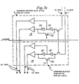
- the programmable timer/event counter of Figures 12c and 12d is an 8 bit binary counter with a programmable prescaled clock source.
- the basic elements comprising the programmable timer/event counter are: 1) a fixed divide-by-8 pseudorandom shift-counter 26 for which the output 0/8 is an internal input 26i divided by 8; 2) a 5-bit prescaler 26a (binary decrementor) which resides in the memory map of Figure 2a as part of the timer control register at P3, (latch 26a'; these 5 bits of 26a' are write only); 3) A 5 bit control latch (write only) 26a-1; 4) 8 bit time value register (timer decrementer) 26; 5) 8 bit timer latch 26b; and 6) an 8 bit capture latch 26c.
- the two accessible locations P2 and P3 ( Figure 2) for the timer function differently at read vs. write, as seen in Figure 12d.
- the location P2 "timer data” contains an 8 bit, write-only latch register 26b-1 and an 8-bit read-only register 26b-2. Note during a read operation, the location P2 will contain the instantaneous count-down value.
- Figure 12d shows the control register at location P3; here, for write, bit position 7 is the "counter start” command position. A "1" written in bit position 7 will immediately start the timer. Bit position 6 of Figure 12d designates the timer source.
- a "1" in bit position 6 selects the internally generated PHI/8 (internal clock frequency divided by 8) clock; a "0" selects the external clock source obtained from bit position 7 in the A port.
- Bit positions 4-0 of the control register 26b, location P3, contain the prescaler 26a latch value for a write operation.
- all 8 bits of the timer control register of Figure 12d contains the capture latch value.
- Figure 12d illustrates the contents of the timer data registerP2. Note that in the read mode, the current timer value will be read. However, in the write mode the data written will determine the current latch value. Any number from 0 to 255 can be written into the timer latch. Likewise, the prescale latch can be loaded with any number from 0-31.
- the timer source bit position 6 and a start/stop bit position 7 are also reloaded when loading the prescaler 26a. As long as the start/stop bit is equal to "0", neither the prescaler nor the timer can be decremented, thus stopping the timer.
- the start/stop bit position (regardless of whether it was previously a "0" or "1") the following happens: 1) the 5 bit prescaler latch register 26a-1 (that was loaded together with the start/stop bit position) is transferred into the prescaler value register 25a.
- the value register 26a for both the prescaler and the value register 26 for the timer are registers that do the actual decrementing.
- the latch, or capture registers 26a-1 and 26b, do not decrement.
- the timer latch register 26b is also loaded into the timer value register 26 upon start.
- the divide by 8 logic (0/8) value is reset to its initial state.
- the decrement clock inputs to both the prescaler 26a and the timer value register 26 which are then enabled.
- the timer whether in internal or external mode, is prescaled by the 5 bit binary counter 26a.
- the prescaling value is determined by the least significant 5 bits of the timer control register P3, Figure 12d.
- the actual prescale value is equal to the timer control register prescale latch value 26a-1 plus 1.
- a value of hex 88 in the timer controller register i.e.
- the prescaler clock is then used at input 26i to decrement the counter 26.
- the interrupt 2 flag in the I/O control register 25 is set each time the counter value 26 decrements past the 0 value.
- the prescaler 26a will count down pasts 0000 at which time the timer value register 26 is decremented 1 count via 26i and the prescaler value register 26a is reloaded with the contents of the prescaler latch register 26a-1.
- the timer 26 continues to be decremented in this fashion until it counts past hex 00 at which time the timer/interrupt flag (interrupt 2 flag) is set to "1" in the I/O control register 25 and the timer value register 26 is reloaded from the timer latch register 26b starting the full time period over again. If at any time during the countdown period, the timer control register bit position 7 change from a "1" to a "0", the timer stops, ceases decrementing. Upon timer start (a "1" in bit position 7 of the timer control register P3) both the prescaler and timer value register 26a, 26 are reloaded with the full latch contents 26a-1, 26b and the system begins to count normally again. Note that there is no way to stop the timer in progress and resume time from where it stopped.
- This register 26c is loaded from the timer value register 26 whenever the interrupt is active. At the falling edge of interrupt 3, the timer value is loaded into the capture latch. When read, the timer control register P3 contains the capture latch 26c value.
- This capture latch feature provides the capability to determine when an external event occurred relative to the internal timer and is ideally suited for pulse width measurement. Note that if an interrupt is not desired, - interrupts should be totally disabled by the interrupt enable bit or the individual enable bit for interrupt 3 should be disabled.
- the divide-by-8 circuit producing PHI/8 is a psendo-random shift counter clocked on the internal clock (H phases) of Figure 4.
- the output signal 0/8 becomes active after 8 internal clock phases have occurred.
- the other source of clock input is the external clock marked "ECC" input.
- the complex gate circuitry determines which of these two clock sources 0/8 or ECC will be the single clock source for the timer circuitry; this is done by examining the TM and TM signals from the timer control register P3. If the bit 6 of the timer control register is "2", then the external clock source EC obtained from the 7th bit of port A is used, otherwise the signal 0/8 is used as a clock source.
- the processor system includes four 8 bit input/output (I/O) ports, A, B, C, and D. These I/O ports can be reconfigured for each of the different processor modes: single chip mode, peripheral expansion mode, full expansion mode, microprocessor mode, and emulator mode as explained in reference to Figures 2 and 10.
- the I/O configuration during initialization is reset to the single chip mode with four external I/O ports. While two most significant bits in the I/O control register must be "0"s to select the single chip mode, these bits are automatically cleared during reset.
- Port A is an input 8 bit port with high impedance inputs.
- Port B is an 8 bit output only port. When port B is read, the value at the I/O pin is being read.
- Port C and D are 8-bit bidirectional data ports in which each bit can be individually programmed to be input or output. Associated with each bidirectional port is a data register such as P8 or P10 and a data directional register such as P9 or P11. Each I/O bit line can be programmed to be an input or output by setting a "1" in the corresponding data direction register for those lines which are to be outputs.
- a "0" in a bit of the data direction causes the corresponding I/O line to be a high impedance input.
- the data register P4, P6, P8, P10 is used to read and write the I/O lines.
- a "1" in the data register will cause a high on the I/O line if it is programmed as an output.
- I/O port C and bits 4-7 of I/O port B are used for the memory expansion. Port A, Port D and bits 0-3 of Port B are not affected. Specifically port C bits 0-7 and port B bits 4-7 are used for the external memory interface. The I/O lines of port C 0-7 are used to pass multiplex address/data as shown in Figure 10a. Output lines of port B bits 4-7 are used for memory interface timing and control as shown in Figure 10a.
- the peripheral expansion mode memory map is shown in Figure 2b.
- the I/O port C, port D and bits 4-7 of port B are used for the memory expansion. Port A and bits 0-3 of port B are not affected. I/O port C bits 0-7, port D bits 0-7, and port B bits 4-7 are used for external memory interface. 1/O port D bits 0-7 are used to pass the most significant byte of the 16 bit address. I/O port C bits 0-7 are used to pass the least significant byte multiplexed address and data as shown in Figure 10b. The output lines for port B bits 4-7 are used for memory interface timing and control.
- the full expansion mode memory map is shown in Figure 2c.
- the I/O configuration for the microprocessor mode is the same as the I/O configuration for the full expansion mode.
- the processor is placed in the microprocessor mode when the MC pin is tied to Vcc.
- the microprocessor mode is identical to the full expansion mode, except that the internal on-chip ROM 11 is disabled and removed from the memory map of Figure 2d. The revised memory map is shown in Figure 2d.
- the emulator mode is enabled when the MC pin is tied to a high voltage source (+12 volts). In the emulator mode, all on-chip I/O and ROM is disabled and removed from the memory map as shown in Figure 2e.
- the emulator memory expansion interface operates identical to the microprocessor mode memory map interface with the exception of the memory map and the pin-out. Specifically, in the emulator mode, all internal peripheral files (Ports A, B, C, D, timer, I/O control register, ROM) are disabled. Port B bits 7-4 become external memory control outputs. Port B bit 3 serves as an output for INTA, the external interrupt acknowledge. Port C and port D are configured in the same manner as in the microprocessor or full expansion modes.
- the emulator mode can support up to 128 interrupts, either maskable or nonmaskable.
- the interrupt acknowledge INTA line goes low, the external I/O circuitry must place the appropriate interrupt vector on the data bus.
- the interrupt vector transfer is independent of the other memory control signals.
- the interrupt vector is used to form the lower order bit of the memory address which contains the low order bit of the interrupt service routine entry point.
- the entry point vector is multiplied by 2 to obtain the address bit.
- Hex FF is the high order byte of the memory address which contains the entry point address least significant bit.
- the entry point address least significant bit is stored adjacent to the most significant bit.
- the interrupt vector values are equivalent to the trap opcodes.
- the interrupt vector corresponding to interrupt 2 is hex FD as before.
- the I/0 Port A functions as an input port for the single chip mode, the partial expansion mode, the full expansion mode and the microprocessor mode. During the emulator mode, port A is disabled by the group decode circuitry as previously described.
- bit 7 of information are obtained from the seven pads of the "A Port" (bits 6-0). Actually there is a separate line of circuitry and pad for each separate bit that are identical to the one shown in Figure 13a.
- the signal is transmitted through standard input protection circuitry A-1 and through a device A-2 clocked by H2 and through dual inverters 210 and device 211 activated from the A port enable signal GA generated in the group decode circuitry 27.
- the A port enable GA signal is clocked through device 214 by H2 and transmitted through inverter 215 into a driver 216 clocked by H4. Bit 7 of A port is different from bits 0-6 and serves two purposes.
- the first purpose is merely as the 8th bit of information input just as bits 0-6 and thus is transmitted through similar circuitry, gated by H2, transmitted through inverters 212 and controlled by the A port enable signal GAfrom the group decode circuitry as in A port bits 6-0.
- the bit 7 may be used as the event counter input (ECC) transmitted to the timer circuitry.
- ECC event counter input
- the event counter signal from A7 is transmitted through inverters 217 and further clocked by H1 and H2 into circuitry 218 which latches the occurrence of the event before it is further clocked by H4 through the NOR gate circuitry 219 to the timer as ECC.
- I/O port B serves as an 8 bit output port.
- the full expansion mode and microprocessor mode four bits of port B are external memory controls (CLOCKOUT, ENABLE, RD/WR and ALATCH).
- the emulator mode port B bits 7-4 are external memory controls as before but bit 3 serves as an output for INTA, the external interrupt acknowledge line. In these modes (all modes but the emulator mode) where the 4 bits are used for external memory controls, the other 4 bits are unused. If it is desired to emulate an 8-bit output port, circuitry has been included that allows the user to make use of the four unused bits of port B in combination with 4 bits built externally see Figure 10b or 10c.
- a port B address is output on port C (or port C and D depending on the mode) and external hardware places the bits 0-3 of the memory data bus into the port B bits 3-0 latches and onto the port B pads.
- the hardware further allows port C to output from the memory data bus bits 7-4 into the external 4 bits of port. Bits 0-3 of the memory data bus, is also output from port C, but are not used externally if the 4 internal B port bits are used. It should be noted that the data output on port B is latch data and thus can be read.
- the port B address is sent out to port C and hardware allows only the external port B bits 3-0 or the contents of their data latch to be read onto the memory bus, and allows only port C bits 7-4 to be read from the external port B onto the memory data bus.
- bit 7 input is the clock or phase H3
- bit 6 input is the enable line
- bit 5 input is the read/write signal (BWRB)
- bit 4 input is the ALATCH signal.
- Bits 7-4 of MD are clocked through devices 224 by the port B write signal clocked by BWRH4.
- This line is then transmitted through the circuitry 220 as previously discussed which also includes the reset signal (RESET) for clearing the latch and then into complex gate 221 where it is combined with the single chip mode signal line, SCR, and the respective control line and through device 222 onto the pad for the respective bit.
- REET reset signal
- the input can be taken from this bit pad through standard input protection through a device clocked by H2 and inverter and a NOR gate 223 which also receives an input from the single chip mode line. This input can then be read onto the memory bus as shown.
- Bit 3 originates from the memory data bus line marked "MD3" through a gating device 226 which is gated by the read/write line originating from the circuitry below in Figure 13b through a series of gating devices and inverter NAND gate 225 which serves the purpose to gate the output by H2 or during a reset operation to change the gate to an input mode.
- the signal is then transmitted to the gate circuit 227 which receives inputs from the INTAX signal used during the emulator mode as a interrupt acknowledge and also the emulator mode signal EM. Since B3 serves this external acknowledge purpose in the emulator mode, the output from this complex gate 227 is then transmitted through device 228 onto the bit 3 pad.
- the input from the bit 3 pad is transmitted through the input protection circuitry, clocked by H2 through an inverter, then into a NOR gate 229 which also receives an input from the emulator mode in order to disable the input line during the emulator mode.
- the bits 2 to 0 of the data bus are input through a gating device 230 which is gated by BWRH4 from the circuitry contained below and through the circuitry 231 which clocks the output onto the respective pads and resets the port to input during a reset condition.
- the output signal during the output mode is then transmitted through device 232 onto the respective pad.
- the input from the respective pad is transmitted through the input protection circuitry as before, and gated by H2 through two inverters onto the memory data bus lines for bits 20 marked MD (2-0) and clocked by BRDH4.
- SCR is the OR of the SC and the reset signal from the interrupt logic circuitry.
- GB and LNGWR are the B port enable line and read/write line from the memory control circuitry.
- GB is clocked by H2 and is an input to NOR gate 233 along with LNGWR which is then transmitted through device 235 clocked by H4 to produce the output or write signal BWRH4.
- the GBP signal is input into NOR gate 234 together with the inverted LNGWR signal (BWRB) and then transmitted through device 236 clocked by H4 to produce the input or read signal BRDH4.
- port C is an 8 bit I/O port with one address for data and one address for port direction.
- setting a bit in a port direction will determine whether that bit in port C is in input bit or an output bit.
- setting the direction latch to "1" sets the corresponding bit position of the port into an output mode.
- the signals CDATAOUT from the memory control circuitry enables port C to output an address in the first state of a long read or write cycle and then if in an output mode, allows port C to output the contents of the data latch onto the port C bit pads.
- bits 7-to-0 of the data from the memory bus is clocked through device 237 into the data latch circuitry 238.
- the data is then transmitted through the complex gate circuitry 239.
- the circuitry 239 also receives the address, BADD (7-0), from the address bus together with the CDATAOUT signal from the memory control circuitry as previously mentioned.
- This data (or address) is then transmitted over the line marked CDATAB (7-0) to device 240 which also receives an enabling signal CHIZ.
- the enabled output is then transmitted to the C port pads.
- CHIZ originates from a circuitry containing a direction latch.
- the direction latch inputs originate from the memory bus on 7-to-0 lines MD (7-0) clocked through gate 241 by COWRH4 into the direction latch circuitry 242. Note that the direction latch circuitry also receives the reset signal from the interrupt circuitry. This reset signal resets the data latch for each bit to the input mode as previously explained.
- the output of the data latch is DIRC (7-0).
- the reset signal also is input into the complex circuitry 243 together with DIRC (7-0) from circuitry 242.
- Complex circuitry 243 also receives PTCOUT and SC.
- SC is the signal for the single chip mode and during the single chip mode PCOUT is disabled allowing the contents of the direction latch to determine the port direction.
- PTCOUT is enabled and places port C into an output mode in both states of a long write cycle and input mode in the first state of a long read cycle.
- PTCOUT originates from the memory control circuitry. Inputs from port C originate on the pad for the respective bits 7-0 and are transmitted through the input protection circuitry through a device clocked by H2 and an inverter into complex gate 244.
- the input data CPADP (7-0) is gated with DIRC (7-0) from the directional latch 242 and is read through device 246 onto the memory bus MD (7-0) clocked in by CERDH4 through device 247. Also the same line to the memory data MD bus can be used to write the data contained in the port C latch 238 which has been gated with the directional latch 242. This enables the user to read the data that is being output or stored in the output latch.
- the devices 248 and 249 are clocked by a single EXTRDH4 which is used in any nonsingle chip mode to read the C port pads onto the memory data bus in state 2 of a long memory read cycle if a valid external address is provided.
- port B enable signal GB is active and does not allow the bits 3-0 of Port C to be read onto the MD bus via NOR gate 250.
- These 4 bits are contained in the internal B port and read onto the memory data bus MD (3-0) as previously discussed.
- the EXTRDH4 signal is produced by the inputs from the memory control circuitry including SC, single chip mode, EXTC signifying an external operation, and LNGWR for the read/write operations. These signals are combined in NOR gate 251 and then clocked by H4 in device 252.
- CEWRH4 is the output signal for the data and is used to clock device 237 to transfer data from the memory data bus into the port C data latch 238.
- This signal originates from complex gate 253 which receives inputs from the single chip signal signifying a single chip mode and from the port C enable signal from the group decode circuitry, GC, BAO from the memory control circuitry signifying a data operation and LNGWR from the memory control circuitry signifying a write operation.
- the signal from 253 is then transmitted through device 254 clocked by H4.
- the directional or control information is written into the directional latch 242 through device 241 clocked by COWRH4.
- COWRH4 originates from NOR gate 255 which receives inputs from the decoder circuitry in a form of GCP, BA indicating a write operation into this latch, and LNGWR signifying a write operation.
- the output from gate 255 is transmitted through device 256 clocked by H4.
- CERDH4 is the signal that enables the input data from port C to be input on the memory data bus, MD (7-0) through device 247 and originates from NOR gate 257 which receives inputs from GCP, BA, and BWR which is the negated LNGWR signifying a read operation.
- the output of gate 258 is then transmitted through device 257, clocked by H4.
- CORDH4 is used to input the contents of the direction register 242 through device 245 onto the memory data bus MD (7-0) and originates from NOR gate 259 which receives inputs of GC, BAO and BWR.
- the output of gate 259 is transmitted through device 260 clocked by H4.
- port D is similar to port C in that it is a bidirectional I/0 port that contains a directional latch and a "1" set in the latch for a corresponding bit the output mode.
- port D is the same as the single chip mode. However, in the microprocessor mode full expansion mode and emulator mode, port D serves as a 8 bit high address output.
- the output information is obtained from bits (7-0) of the memory data bus MD and transmitted through device 261 clocked by signal DEWRH4. This information is transmitted through the data latch 262 into complex circuitry 263.
- the complex circuitry 263 also receives inputs from the data bus address line BADD (F-8) and DADOUT which allows port D to output the high address, BADD (F-8), during the emulator mode, microprocessor mode and full expansion mode.
- the output from complex gate 263 is then transmitted through device 264 onto the D port pads. Similar circuitry exists for each of the 8 pads. Device 264 is disabled when that bit position is in the input mode determined by the direction latch 266.
- the contents of the direction latch for each of the bit positions is read from the memory bus MD (7-0) gated by DOWRH4 in device 265 into the direction latch 266.
- the output of the direction latch is transmitted into complex gate 267 which is combined with the reset signal also input into the directional latch together with the DADOUT signal previously discussed.
- the output of complex gate 267 is DHIZ which is the disabling signal for the device 264.
- Two sets of information can be read from port D.
- the contents of the direction latch is output by the line marked DIRDB (7-0) through a device 268 gated by DORDH4.
- the input from the D port pads is transmitted through the input protection circuitry clocked by H2 and through an inverter into complex circuitry 270 which also receives the contents of the directional latch. This enables the user to read the input from the pad or the information contained in the output data latch 262 determined by the information for that bit contained in the direction .latch.
- the output of this complex gate is then transmitted through device 271 and through device 269 clocked by the signal DERDH4 onto the memory data bus.
- the signal DEWRH4 (write data into data latch) used to gate device 261 is produced in NOR gate 272 from the enable D port signal, GDP, LNGWR and BAO, all from the memory control circuitry. BAO signifies a write operation into the latches contained in port D.
- LNGWR signifies a write operation or output operation from port D.
- the output from gate 272 is transmitted through device 273 clocked by H4.
- DOWRH4 is the signal to enable device 265 to enable the user to write into the direction latch 266 and is produced in NOR gate 274 from signals GDP, BAO and LNGWR.
- the output of NOR gate 274 is transmitted through device 275 clocked by H4.
- DORDH4 is used to enable the output of the contents of the direction latch onto the memory bus and is produced in NOR gate 276 from the signal GDP, BWR from port C and BAO.
- the output of NOR gate 276 is transmitted through device 277 clocked by H4.
- DERDH4 is the signal used to clock device 269 to allow the output of either the contents of the port D data latch 262 or the inputs from the port D input pad and originates from NOR gate 278 which has signals GDP, BAO, and BWR.
- the output of gate 278 is transmitted through device 279 which is clocked by H4.
- the buffers 222, 228, 232 for the B port may be conventional MOS output buffers, while the buffers 240 and 262 for the C and D ports may be conventional tri-state MOS output buffers.
- a microcomputer 10 constructed according to the invention may contain a self-test procedure as set forth in U.S. Patent 4,158,431 issued to Van Bavel et al, assigned to Texas Instruments.
- the procedure of patent 4,158,431 consists of exercizing all of the display characters 13-1 and keys 13-2 as well as all of the I/O devices on the D port of Figure 10a, all under control of a sequence of macroinstructions in the ROM 11 as manufactured.
- This self-test procedure establishes that all of the external elements of the system are working and gives some indication that the chip 10 itself is fully functional, but this is not an exhaustive check. Prior to connecting into such a system, however, functional testing must be done.
- the microcomputer 10 may employ a test method in which a two-type macro-code is fixed in the ROM 11 upon manufacture and used to check the remaining macro-code.
- This two-byte code is different for each ROM code or program and represents some function of all of the other bytes coded in the ROM. For example, it might be the LSB's of the sum of all the other bits in the ROM, or preferably some other function which provides a multiple check of all bits.
- This two-byte code is referred to as a cyclic redundancy code or CRC and is a 16-bit value which is a function of every bit of data used to create it.
- the CRC is calculated using every byte of the macrocode in the ROM except the CRC itself which is stored at a location such as F802 and F803 in a 2048 bit ROM 11 or F002 and F003 in a 4096 bit ROM 11.
- This test program is loaded into the RAM 12 of the chip 10 while the chip is in the microprocessor mode ( Figure 2d) or in one of the expansion modes ( Figure 2b or 2c), by a sequence of move double MOVD or move MOV instructions.
- MOVD %7D02, R1 in the microprocessor mode places the first two bytes of the object code of the test program in RF locations R10, R11. In this manner, all of this code is stored in RAM 12, and then a MOV%00, P1 instruction returns the microcomputer 10 to the single-chip mode of Figure 2a, with the address of R10 in the program counter PCL so execution of the test program code begins.
- the original code from F902, F903 is compared with the computed value, and the comparison output on C and D ports.
- About 890,000 machine states are needed by the microprocessor 10 to execute this test program, but this is all internal; the test machine does not need to store unique codes and off-chip accesses are not needed for the bulk of the test.
- microcomputer described in detail herein is in the form of an N-channel silicon gate integrated circuit in a single silicon chip.
- features of the invention can be used in devices made by other processes such as metal gate, P-channel, CMOS, silicon-on-sapphire, and the like.
- the memory 11 has been described as a ROM of the fixed-program type, but of course an electrically-programmable ROM or electrically-erasable ROM may be used.
- the ROM 11 is referred to as a program memory and the RAM 12 as a data memory, and these are the primary functions in many applications; it is understood, however, that "data" from the ROM 11 is used in some algorithms ("data” being numerical constants and the like), .and that the device can execute instruction codes from the RAM 12, or program blocks can be down-loaded into RAM 12 from external tape or disc drive, or from a telephone coupler, for example, and executed from RAM 12. Furthermore, additional control lines and functions such as READY, HOLD, bus-status code, etc. as in said application S.N. 210,109 may be used in a device having features of the invention.
Description
- This invention relates to integrated semiconductor devices and systems, and more particularly to features used in an electronic digital processing system of the single-chip microprocessor or microcomputer form.
- A microprocessor device is a central processing unit or CPU for a digital processor which is contained in a single semiconductor integrated circuit, usually fabricated by "MOS/LSi" technology, as shown in U.S. Patent No. 3,757,306 issued to Gary W. Boone and assigned to Texas Instruments. The Boone patent shows an 8-bit CPU on a chip including a parallel ALU, registers for data and addresses, an instruction register and a control decoder, all interconnected using a bidirectional parallel bus. U.S. Patent No. 4,074,351, issued to Gary W. Boone and Michael J. Cochran, assigned to Texas Instruments, shows a single-chip "microcomputer" type device which contains a 4-bit parallel ALU and its control circuitry, with on-chip ROM and RAM for program and data storage. The term microprocessor usually refers to a device employing external memory for program and data storage, while the term microcomputer refers to a device with on-chip ROM and RAM for program and data storage; the terms are also used interchangeably, however, and are not intended as restrictive as to this invention.
- Subsequent to 1971 when Patents 3,757,306 and 4,074,351 were originally filed, many improvements have been made in microprocessors and microcomputers to increase the speed and capability of these devices and reduce the cost of manufacture, providing more circuitry in less space, i.e., smaller chip size. Improved photolithographic techniques allow narrower line widths and higher resolution, providing added circuit density, but circuit and system improvements also contribute to the goals of increased performance with smaller chip size. Some of these improvements in microprocessors are disclosed in the following U.S. Patents, all assigned to Texas Instruments: 3,991,305 issued to Edward R. Caudel and Joseph H. Raymond Jr.; 4,156,927 issued to David J. McElroy and Graham S. Tubbs; 3,934,233 issued to R. J. Fisher and G. D. Rogers; 3,921,142 issued to J. D. Bryant and G. A. Hartsell; 3,900,722 isued to M. J. Cochran and C. P. Grant; 3,932,846 issued to C. W. Brixey et al; 3,939,335 issued to G. L. Brantingham, L. H. Phillips and L. T. Novak; 4,125,901 issued to S. P. Hamilton, L. L. Miles, et al; 4,158,432 issued to M. G. VanBavel; 3,757,308 and 3,984,816.
- Additional examples of microprocessor and microcomputer devices in the evolution of this technology are described in publications. In Electronics, September 25,.1972, p. 31-32, a 4-bit P-channel MOS microcomputer with on-chip ROM and RAM is shown which is similar to Patent 3,991,305. Two of the most widely used 8-bit microprocessors like that of Patent 3,757,306 are described in Electronics, April 18,1974 at pp. 88-95 (the Motorola 6800) and pp. 95-100 (the Intel 8080). A microcomputer version of the 6800 is described in Electronics, February 2,1978 at pp. 85-103. Likewise, a single-chip microcomputer version of the 8080 is shown in Electronics, November 25,1976 at pp. 99-105 and a 16-bit microprocessor evolving from the 8080 is described in Electronics, February 16, 1978, pp. 99-104. Another single-chip microcomputer, the Mostek 3872, is shown in Electronics, May 11, 1978; at pp. 105-110. An improved version of the 6800 is disclosed in Electronics, September 17, 1979 at pp. 122-125, while a 16-bit microprocessor identified as the 68000 which evolved from the 6800 is described in Electronic Design, September 1, 1978 at pp. 100-107.
- US―A―3,900,054 (Perlowski) discloses a microprogramming apparatus for a data processor using a diode matrix to translate an operation code of a macfoinstruction into an address of a ROM storing microinstructions.
- US-A-3,980,991 (Mercurio) describes an electronic computer in which a jump in a microprogram is executed in dependence upon the state of a selected one of a plurality of bistable circuits. The states of the bistable circuits are set either in response to the execution of microprograms by the computer or in response to whether or not a logical condition specified by a microinstruction has been met.
- The technology of integrated circuit design and manufacture has progressed to a point where virtually any electronic system having digital processing or control functions can employ a microcomputer or microprocessor chip. The cost of designing and manufacturing the devices is a limiting factor, however. Semiconductor manufacturing is oriented toward production of large quantities of a single device type, rather than production of a few of many different specialty items, and so to be economical a chip design must be adaptable for a wide variety of uses, not only by changing the ROM code but also by providing many input/output options and similar features. Thus, a device as in Patent 3,991,305 has been manufactured in quantities of millions of units for many different electronic calculators, electronic games, appliance controllers, and the like. Not only the semiconductor manufacturing cost is minimized by use of the same device, but also the design cost is minimized because very little circuit design is needed (only external to the chip) and the programming effort employs an instruction set and commonly-used subroutines and algorithms in which a high level of experience is acquired. Nevertheless, the design cost for using a microcomputer device in a new application may be prohibitive even though only assembly language programming is needed, this software cost is unduly high because of the number of different and incompatible programming languages used on the wide variety of device types.
- It is the principal object of this invention to provide an improved microcomputer or microprocessor device which is adaptable for a wide variety of uses but yet is constructed to facilitate low-cost manufacture and to minimize programming costs.
- According to the present invention there is provided an electronic digital processor system comprising: internal memory means for storage of data and instructions which define operations on said data and other functions of the system; arithmetic and logic means for performing said operations on said data; register means for temporary storage of said data and temporary storage of addresses for accessing said internal memory means; a plurality of data paths coupling said internal memory means, said arithmetic and logic means, and said register means; and control and timing circuitry means coupled to said data paths, said control and timing circuitry means receiving instructions from said internal memory means via said data paths and generating command signals to said arithmetic and logic means, to said data paths, and to said register means for execution of said instructions to define the operation of the processor system; characterized by peripheral control circuitry means for providing one of a plurality of memory configurations which provide access to said internal memory means while providing offset addressing access to peripheral components including a plurality of multi-bit input/output ports for providing input and output of information for the processor system, said peripheral control circuitry means being coupled to said data paths for transferring addresses and data and receiving command signals from said control and timing circuitry means.
- According to the invention there is further provided a method as set forth in
claim 18. - The novel features believed characteristic of the invention are set forth in the appended claims. The invention itself, however, as well as other features and advantages thereof, will be best understood by reference to the detailed description which follows, read in conjunction with the accompanying drawings, wherein:
- Figure 1 is an electrical diagram in block form of an MOS/LSI microcomputer chip including CPU, ROM and RAM and utilizing features of the invention;
- Figure 2 is a memory map for the logical address space for the microcomputer of Figure 1 and Figures 2a-2e are detailed memory maps like Figure 2 for various operating modes of this microcomputer;
- Figure 3 is a greatly enlarged plan view of the semiconductor chip containing the microcomputer of Figure 1 showing the physical layout of the various parts of the device;
- Figure 3a is an enlarged detail view of a part of the layout of Figure 3 showing the regular pattern of the ALU and register strip;
- Figure 3b is a pictorial view of the microcomputer chip of Figure 3 mounted in a 40-pin dual-in-line package;
- Figure 4 is a timing diagram showing voltage vs. time for various events in operation of the system of Figure 1;
- Figure 5 is a detailed electrical diagram of the CPU, including ALU, shifter S, registers and busses, in the microcomputer of Figure 1;
- Figure 6 is a detailed electrical diagram of the control ROM used in the microcomputer of Figure 1;
- Figure 7 is a map of the relative locations of the Figures 7a-7f;
- Figures 7a-7f are electrical schematic diagrams of various parts of the ALU and register strip within the CPU of the microcomputer of Figure 1;
- Figures 8a-8j (six sheets) show a logic flow chart of the execution of the microinstructions of Tables B and C in the microcomputer device of Figure 1;
- Figure 9 is a map of the opcodes for the macroinstructions of Table A executed by the microcomputer of Figure 1;
- Figures 10a-10d are electrical diagrams of microprocessor systems using the
microcomputer chip 10 of Figure 1 in various operating modes; - Figure 10e is a timing diagram for operating modes of Figures 10b-10d;
- Figure 11a is a table illustrating the group decode circuit bus addresses which product peripheral activating signals;
- Figure 11b is a table illustrating the operating mode specifications for the different memory configurations of Figures 2 and 10;
- Figure 12a is a table listing the interrupt vector locations in memory;
- Figure 12b is a table illustrating the input/output control register contents;
- Figure 12c is a conceptual block diagram of the programmable timer/event counter;
- Figure 12d is a table illustrating the contents of the timer data register and the timer control register;
- Figure 13a is a schematic diagram of the A port;
- Figure 13b is a schematic diagram of the B port;
- Figure 13c is a schematic diagram of the C port;
- Figure 13d is a schematic diagram of the D port;
- Figure 13e is table illustrating interrupt generation for the system emulator mode. Detailed description of specific embodiment
- With reference to Figure 1, a
microcomputer chip 10 is shown which employs features according to one embodiment of the invention. Thechip 10 is a semiconductor integrated circuit of the MOS/LSI type including a silicon bar of less than about 200 mils on a side, mounted in a standard 40-pin package. Totally contained within thechip 10 is a digital processor having a ROM or read-only memory 11 for program storage and a RAM or read/write memory 12 for data storage, along with aCPU 13. The CPU consists of an arithmetic logic unit orALU 14 with its workingregisters 15 and busses 16, along with a control ROM orCROM 17 for generating microinstructions or control signals onlines 18. TheCPU 13 accesses the ROM andRAM memory ALU 14, theregisters 15 and the ports, although of course concepts herein described would be applicable to 4-bit, 16-bit or 32-bit devices, for example. - The
registers 15 in theCPU 13 include an instruction register IR, a status register ST, circuitry BCD for binary-coded-decimal constants, a shift circuit S which receives the output of theALU 14, a register T/MAH which functions as both a temporary store for operands and for the high order byte of the memory address (memory address high), a sixteen bit program counter split into two eight bit registers PCH and PCL (program counter high and low); a stack pointer SP, and a memory address low register MAL. Address buffers 19 generate true and complement address signals on busses AH' and AL' from the address busses AH and AL. Operands are for the most part stored in theRAM 12 which functions as a register file RF, rather than intemporary registers 15 associated with theCPU 13. - The
busses 16 interconnect thevarious registers 15, theALU 14 and MD, AH' and AL' busses. TheALU 14 always receives a P input from a P bus and an N input from an N bus, and produces an output via shifter S to an output or O bus. Access to these P, N and O busses 16, to theregisters 15 andALU 14, and to the MD, AH and AL busses is controlled by the control signals 18 from theCROM 17. - The
microcomputer chip 10 operates on the basis of 8-bit macroinstruction words stored in theROM 11 and transferred to the instruction register IR one at a time. One example of a macroinstruction set executed in theCPU 13 is described in Table A which will be discussed in detail below. The Table gives the instruction word in mneumonics, also referred to as assembly language or source code, and also gives the machine-language opcode in binary (this is like object code except object is in hex). Usually an opcode plus one or more address bytes are used to execute an instruction. An instruction word or opcode held in IR is an input to anentry point circuit 21 which produces an 8-bit address vialines 21 a to addresscircuitry 22 for theCROM 17, accessing one of 256 possible CROM addresses (in the example embodiment) to producesignals 18 defining a microinstruction as set forth in Tables B and C, to be described below. One macroinstruction of Table A produces a sequence of microinstructions. A part of each of the microinstructions (i.e. some of outputs 18) is used to generate the next CROM address; a microjump address is fed back to the entry point circuit vialines 23, and dispatch control information is fed back vialines 24, as will be explained. Thus, a sequence of microinstructions is generated from each macroinstruction in IR, also dependent upon status bits in the status register ST and other conditions. Addresses for operands, if needed, are contained in words fromROM 11 following the opcode and are transferred to MAL or MAH while the opcode stays in IR during this sequence. - A map of the logical address space for the microcomputer of Figure 1 is shown in Figure 2. The example embodiment employs 8-bit AH and AL addresses, providing a 16-bit address, and so 216 or 65,536 bytes are available in this space (often referred to as "64K" bytes where one "K" is 1,024). The addresses are shown in four hexidecimal digits, ranging from the
first address 0000 to the last FFFF. In this description memory addresses will be given in hex, unless noted. A page is 28 or 256 bytes, i.e. all addresses on a page are defined by AL and the page is selected to AH. Themicrocomputer 10 uses the zero page (addresses 0000 to OOFF) for the register file RF inRAM 12, the "one" page (addresses 0100 to 01 FF) for the peripheral file PF, and the FO to FF pages (addresses FOOO to FFFF) for the program memory ofROM 11. Some of these spaces for RF andROM 11 may not be populated, depending upon the size of the ROM and RAM chosen. Other space such as 0200 to EFFF is available for the expansion modes as will be explained. - In the microcomputer of Figure 1, the control circuitry responsive to the AH' and AL' busses and control
bits 18 defines the way in which theCPU 13 accesses the peripheral file PF including external ports, timer, reset and interrupts, as well as memory control. An I/O and interrupt control register 25 atmemory location 0100 of Figure 2 is loaded directly by the MD bus and is part of the ALU/register strip; this register contains two memory mode control bits which define the memory expansion modes as will be described, as well as interrupt masks and flags. A programmable timer and event counter is also included in this peripheral control circuitry, and comprises acounter 26, aregister 26a which functions as start/stop control, input select and prescaler, acontrol 26b, and acapture latch 26c. These elements of the timer are accessed by the MD bus and are eight bits wide, so are advantageously constructed as part of the ALU/register strip. Thecounter 26 is a fixed divide-by-8 pseudorandom 8-bit shift counter which simply divides its input by eight. The input to thecounter 26, which may be an internal clock or an external clock or event, goes through the prescaler part of theregister 26a which is an additional 5-bit divide-by-N counter loaded (via a prescale register) from the MD bus with any number up to thirty-two. The 8-bit timer register 26g is loaded from MD with the desired final count, up to eight bits or 256. When this count is reached, an interrupt INT2 is signalled. The instantaneous count may be read out on MD via the 8-bit capture latch 26c without stopping an ongoing count in thecounter 26; this is instigated by INT3. - In this peripheral control circuitry, a
group decode circuit 27 andmemory control circuit 28 receive the AH' and AL' address bits and three control signals 18 (#MEM, #WR and #MEMCNT) and produce controls which select between theROM 11,RAM 12, ports A, B, C or D, the timer or I/O control, etc. for access by a given address. Only one of these is activated in any one cycle. The group decode 27 andmemory control circuitry 28 likewise generate commands for controlling and/or selecting functions as will be explained. - Two interrupt input pins INT1 and INT3 are provided, in addition to the timer interrupt INT2. These inputs are connected to interrupt
control circuitry 29 which is also responsive to the contents of theregister 25. A reset input RST is used to zero or initialize the microcomputer, overriding any function or interrupt. - A mode control input pin MC connected as an input to the peripheral control circuitry provides a selection of the operating modes (along with the internally-loaded bit-7 and bit-6 of the I/O control register 25). Figures 2a to 2e are memory maps showing the unique parts of the address space for these modes; the register file address space RF remains the same as Figure 2 for all modes. The modes are: (1) single-chip microcomputer mode where all memory is on-chip in the
ROM 11 andRAM 12 as in Figure 2 and the peripheral file PF is configured as in Figure 2a, this being the primary mode of operation; (2) a peripheral expansion mode of Figure 2b where some additional off-chip circuitry may be accessed in the PF space via ports B and C; (3) a full expansion mode of Figure 2c where almost 64K bytes of off-chip memory may be accessed by ports B and C, the RF and ROM being the same as Figure 2; (4) a microprocessor mode of Figure 2d where the on-chip ROM 11 is ignored and all program memory is off-chip, but the on-chip RAM 12 is used as Figure 2; or (5) the emulator mode of Figure 2e in which both the peripheral file PF and the on-chip ROM 11 are disabled and all I/O and program memory is off chip, accessed by ports B and C with the on-chip RAM 12 or RF being used as in Figure 2. The various modes allow a wide variety of different functions to be provided by one basic chip type without design, layout or microcode modifications, thus greatly reducing the cost. Input/output buffers 30 connect the ports A, B, C, D to the MD bus, as defined by direction control registers P7, P9, P11, for some modes and by the mode control arrangement via group decode 27 andmemory control circuitry 28. - One of the important features of the microcomputer chip of Figure 1 is that the
RAM 12 is of the dynamic type using one-transistor cells with transparent refresh. On-chip RAM for microcomputers is usually of the static or pseudo-static type; if the RAM is of the dynamic type as in Patent 4,074,351, then the refresh function may interfere with access by the CPU. In contrast, the microcomputer of Figure 1 contains arefresh address counter 31 which is self-incrementing and may produce a new 5-bit row address to the row address decoder 12X every machine cycle, so one row of the RAM is accessed for refresh if none is accessed by the CPU. If amemory 12 access cycle is occurring, however, thecounter 31 is not incremented and the refresh address output of thecounter 31 is not applied to the decoder 12X. TheRAM 12 is of the folded-bit-line type with a memory bit and its complement on opposite sides of sense amplifiers 12S; i.e., dual memory bits are employed instead of dummy cells traditionally used in dynamic RAMs. In the 128 byte RAM of the example, 128x8 or 1024 bits are needed, and with two one-transistor cells per bit theRAM array 12 has 2048 one-transistor cells. The array is partitioned 32x8x4, so the X decoder 12X is a one-of-32 select, the Y decoder 12Y is a one-of-4 select for each of the eight input/output bits of the RAM, and thirty-two sense amplifiers 12S are used. Of course, the RAM size can be doubled to use the whole zero page of Figure 2, in which case 256x8x2=4096 cells are needed. - In Figure 3, the microcomputer of Figure 1 is illustrated in chip layout form. A major part of the area of the
chip 10 is occupied by the memory including theROM 11 andRAM 12 with their address decoders. TheROM 11 has associated with it an X address decoder 11X and a Y address decode and ROM data output circuit 11y of conventional design; eleven address bits are used to define one of 2048 eight-bit bytes in the ROM (twelve bits if a 4096 byte ROM is employed), so an address for the ROM needs both the MAL and MAH registers, i.e., address bits from both AL and AH busses. The RAM has an X address decoder 12X which selects 1-of-32 row lines, and a Y address decoder 12Y which selects 1-of-4 column lines, so only seven bits are needed for the RAM select (eight if a 256 byte RAM is used). Another major part of the chip area is thecontrol ROM 17 and its associated X andY decoders output buffers 17b. If fully populated, the number of bits in the control ROM would be 256 times the number of output lines 18. Only forty-fiveoutput lines 18 are needed for the example instruction set of Table A, and only 160 microinstruction addresses as in Tables B and C, so the control ROM is only 160x45 or 7,200 bits. The output ports A, B, C, and D each have eight bonding pads on the chip (total of thirty-two) for connection to external, and the areas of the chip around these bonding pads are occupied by thebuffers 30 used for the ports. It will be noted that the port A is only used for input, so the space needed for the input buffers for this port is much less than for the remaining ports B, C, and D which require tri-state output buffers. - Between the
ROM 11 and the CROM buffers 17b on thechip 10 of Figure 3 is the "strip" which is an array of rows (parallel to control lines 18) and columns (parallel withmetal bus lines 16 and register/ALU bits 14,15) containing all of the 8-bit registers, ALU bits, and like circuitry associated with thebusses 16 andcontrol lines 18. As set forth in prior application S.N. 210,109, filed November 24, 1980 by McDonough, Guttag and Laws, assigned to Texas Instruments, an important feature is that theALU 14 and its associated registers IR, ST, S, T/MAH, PCH, PCL, SP, and MAL us described above are laid out on the MOS/LSI chip 10 in a regular strip pattern as seen in Figure 3. Other circuitry connected to the busses and havingcontrols 18 shared by eight bits is also in the strip, such asentry point 21, address buffers 19,timer 26, I/O control register 25, etc. Each of these registers as well as the ALU contains eight bits or stages which are laid out in a pattern like memory cells, the bits arranged horizontally and aligned vertically as seen in Figure 3. The MD, AL, AH, O, N and P busses of Figure 1 are each eight parallel metal strips on top of the cells of the ALU and registers (rather than beside the registers as depicted in Figure 1), and all of the dozens ofcontrol lines 18 are horizontal polysilicon lines typically used as the control gates for transistors in theALU 14 and its registers and like circuitry. The number ofcontrol lines 18 needed for theALU 14 is greater than for a single register such as the MAL register, for example, and conveniently the space needed to lay out the ALU stages is greater than for a single register, so waste space in minimized. That is, the space needed in thecontrol ROM 17 to generate thecontrols 18 is about the same as the space needed for the controlled circuitry. This layout arrangement is indeed advantageous because the ALU and registers fit alongside the control ROM with virtually none of the wasted space used merely for routing conductors in conventional construction of microprocessors. All bus lines MD, AL, AH, O, N and P, and allcontrol lines 18 are routed over functional regions or cells of the chip rather than over unused silicon, and almost all 90 degree turns are produced inherently at functional cells rather than in conductor routing. In the prior devices, the control ROM, the registers, the ALU, etc., were islands of circuitry connected by busses or conductors. The enlarged view of Figure 3a shows a small part of the strip, two-bits wide, illustrating the metal bus lines and thepolysilicon control lines 18 for an N-channel silicon gate MOS device made generally by a single-level polysilicon process according to U.S. Patent 4,055,444, assigned to Texas Instruments. Various contacts (not shown) would be made within each register bit or stage from metal to silicon or to polysilicon. It is significant to note that most of the connecting lines from registers to busses illustrated in Figure 1 are not physically lines or elongated conductors at all but instead are merely metal-to-silicon or metal-to-poly contact areas along the metal bus lines of Figure 3a. That is, routing of 8-bit sets of parallel conductors is minimized by the strip feature, and the size of thechip 10 is reduced. Thebusses 16 are staggered so that all six busses are not needed in any one part of the strip, and thus the pitch or maximum width of cells of the strip is minimized since the metal-to-metal spacing is a critical limiting factor in bit density. To this end, the placement of theregisters 15 is such that the N bus need not co-exist in any register with the AL or AH busses, and the P bus ends where the AL bus starts, as illustrated in Figures 1 and 3a. Some of the clocks needed in the registers and ALU of the strip are run in metal lines like the busses 15 (H1 shown in Figure 3a) so these place further constraints on the density and make the strip concept and bus/register optimum placement more significant. Connections from MD to P or N busses are made by transistors located in the strip like a register and labelled MDtP, MDtN; since this logic requires eight parallel bits of transfer gates, tied to sets of eight parallel busses, and using CROM outputs 18 as controls, it fits well in the strip. - The
CROM 17 fits alongside the strip to provide thecontrols 18 in the control-intensive areas of the ALU and register/bus connections, and alongside theentry point circuitry 21 where the address control and jumpaddress lines microcomputer 10 particularly easy to modify by changing the micro or macrocode. - The
microcomputer 10 may be modified at three levels, plus the mode control. The first level is changing the ROM code of theROM 11, and of course this is the most widely practiced modification. The ROM code is defined by a single mask in the manufacturing process as set forth for example in U.S. Patents 3,541,543, 4,208,726 or 4,230,504, assigned to Texas Instruments. The macroinstruction set may be supplemented (keeping basically the same microinstruction set), or the microinstruction set may be changed, both of these levels requiring changes in theCROM 17 code upon manufacture. The CROM code is defined by a single mask in manufacture, just as the ROM code, so physically it is just as easy to change the microinstruction set; however, the macro assemblers and micro assemblers (computer programs used as design aids for customers) then are different. In addition to these ways of altering thedevice 10, the sizes of the ROM and RAM may be increased to allow more complex algorithms to be programmed in the ROM code, and the size of theCROM 17 may be increased to provide more complex micro- and/or macro-instruction sets. It is important to note that the mode control MC (and bits 6-7 of register 25) allows changes without any type of physical or mask change; no fuse links or the like are needed. - The
microcomputer chip 10 operates from a basic clock frequency referred to as Xtal in Figure 4. This frequency of about 5 MHz is supplied by aninternal oscillator 33 controlled by an external crystal coupled to two pads labelled Xtal in Figure 1 or 3. From the clock Xtal,clock generator circuitry 33 produces four basic overlapping half-cycle clocks H1, H2, H3 and H4 for each microinstruction cycle or state time S1, S2, etc., as seen in Figure 4. Each state time equals two complete cycles of the clock Xtal. H4 overlaps two state times. - Short memory cycles to access the
RAM 12 are completed in one state time such as S1 of Figure 4; #MEMCNT is low and all bits of the AH bus are low during H1, and the RAM address is valid on the AL bus while #MEM is high. The write control #WR is high for write or low for read. The data accessed is then valid on the MD bus during H4 at the end of the cycle, extending over into the beginning of the next cycle, so the data may be loaded into the registers T or IR at the end of a cycle or gated onto the P or N busses at the beginning of the next cycle. - All memory references to the register file RF in the
RAM 12 use this short cycle; all other memory references (i.e., to the on-chip ROM 11, the peripheral file PF, and extended memory) require two microinstruction executions and are called long memory cycles as illustrated in Figure 4. For long cycles, the memory continue command #MEMCNT is high during the first state time and low during the second. The memory command #MEM must be high during H1 of both cycles, and the address valid on AH and AL during H1 of the first cycle. For read, the write command #WR is low from the beginning of the first cycle through H1 of the second, and the data is valid during H4 beginning at the end of the second cycle. For long write, #WR is high, and the write data is gated onto the MD bus for H4 of both first and second cycles. - Within a given state time or microinstruction cycle, the address on the AH' and AL' busses becomes valid during H2. This address is based on the address loaded onto AH and AL during H1. In the
ROM 11, the array is precharged during H1 with all row or X lines going to Vss and all column or Y lines going to Vcc, then the ROM X address gated into the array from decoder 11X beginning at H3 and the ROM Y address coming valid at the beginning of H4, so the ROM output is valid at H4. - The
CPU 13 in themicrocomputer 10 of Figure 1 consists of theALU 14, theregisters 15 and thebusses 16 controlled by theCROM 17. In Figure 5 a more detailed block diagram of the ALU and shifter S and the associated busses is shown, and Figure 6 shows theCROM 17 and itsmicroinstruction output bits 18. Control of the ALU and access to the busses is defined entirely by these microinstructions orbits 18, identified in Figure 6 for the illustrative embodiment. An 8-bit address onlines 21a from theentry point circuitry 21 contains a 6-bit X address on lines 21X and a 2-bit Y address on lines 21Y. The lines 21X are connected toX decoder 22X which selects one of up to 64 X lines in the array of ROM bits of theCROM 17. The lines 21Y are connected to aY decoder 22Y which selects 1-of-4 in each group of four Y lines (only forty-five groups used). Thus, for each 8-bit address onlines 21 a, a different "microinstruction" is output on thelines 18; a microinstruction may have any number of thelines 18 active, but usually a combination of only afew lines 18 is active for a given microinstruction. Eachline 18 goes to abuffer 17b to drive a higher capacitance load than the array output Y line itself would allow, and to clocked gates and other such logic as needed. All microinstruction bits (control lines 18) in Figure 6 and throughout this description are referred to with a prefix "#". Some bits are active low and thus have a minus sign prefix, like #-OtST. In the microinstruction bits of Figure 6, the letter "t" means "to", so #-OtST means "0 bus to ST register", i.e., the gates connecting the 0 bus to the status register are activated by this bit. The eight bit jump address on thelines 23 is denoted #JmpAddr (7-0), while the 3-bit jump control on thelines 24 used for dispatch addressing is denoted #JmpCntl (2-0); these eleven bits are used in theentry circuit 21 to generate the next CROM address. All of the twenty-onebits 18 from #OtPCH down to #ONEtAH in Figure 6 control the access toregisters 15 frombusses 16. Of these, #LowWriteO and #LowWrite1 are decoded to produce pseudo-microinstructions OtPCL, OtMAL and OtSP. The bits #ONEtAL and #ONEtAH place a "1" on the AL or AH busses to generate theB register address 0001 or the PF page address 0100 (hex) in a microinstruction. Default to all 0's on AL and AH is A register address in the register file. Connections betweenregisters 15 and busses 16 are described in detail below. The #MEMCNT bit is a "memory continue" control for long memory cycles; theRAM 12 can be accessed for read or write in one state time, but theROM 11 or peripherals in PF require two states, so for this reason control line #MEMCNT is active in the first state of every long memory cycle as seen in Figure 4. #MEMCNT is used to form several other control signals, and always identifies the first or second state of a long memory cycle. The #MEM bit signifies a memory cycle and is active wheneverROM 11,RAM 12 or external memory is accessed. The #WR bit is a write command, so if #MEM and #WR are active a memory write condition exists, while if #MEM is active and #WR is not, a memory read condition exists. The #-LST signal is a load status command for ALU operations; the status register ST can also be loaded from the 0 bus by the #-LST command. The ALU is controlled by nine bits labelled #ShiftCntl (3-0), #AluCntl (3-0) and #ABL; these controls will be described below in detail. - The
microinstruction bits 18 are physically arranged in the order used in Figure 7a-7e rather than in the order shown in Figure 6, so that acontrol bit 18 is generated as close as possible to the point it is used in the strip. - The microinstruction control of access to the
registers 15, busses 16 andALU 14 will now be described in reference to Figures 5, 6 and 7a-7f. - The P bus is one of the inputs to the
ALU 14. It is called 'P' for "Positive", because in a subtract operation where theALU 14 only computes P N the P bus contains the positive, or left-hand, operand. The P bus is loaded from the MD bus viatransistors transistor 16d (Figure 7b), loaded from the PCH register viatransistor 16e, or from the PCL register viatransistor 16f. Any of the AL bus sources may be placed on the P bus by gating them on the AL bus and asserting the #PAL microinstruction bit going to the gate oftransistor 16d, connecting the P bus to the AL bus. If no source is specified, i.e., "default", the P bus assumes the value of all zeros. The P bus is loaded in the beginning of a microinstruction cycle, on phase H1. All of the possible P bus sources and the microinstruction bits oroutputs 18 needed for each are as follows:
- The N bus is the other input to the
ALU 14. It is called N for "negative", since on the ALU subtract operation it contains the negative, or right-hand, operand. It is loaded from the MD bus viatransistors transistor 16i, loaded from the IR register viatransistor 16j, the status register ST via transistor 16k, or the BCD constant register viatransistor 16m. It is understood, of course, that there are sets of eight of each of thetransistors 16a to 16j, one for each of the eight bits of each bus and each register. Only four transistors in thesets 16k or 16m are needed. The source of the N bus is indicated directly by a bit in the microinstruction word, as shown below. If the bit is '1', the source is gated onto the N bus. If no source is specified, the N bus assumes the value of all zeros. The N bus is also loaded at the beginning of a microinstruction cycle, on phase H1.
- The AL or address low bus holds the lower eight bits of all memory addresses. This comprises the entire address for references to the register file RF in
RAM 12, or the lower byte for references to the peripheral file PF, on-chip ROM 11 and extended memory in expansion modes. The AL bus is loaded during the- phase H1. The sources of the AL bus are the MAL register viatransistor 16n, the SP register viatransistor 16p, or the constant 01 via transistor 16q. The constant is provided to efficiently addressRAM location 01 which is the "B" register. If no source is specified, "default", the AL bus assumes thevalue 00 which is the A register in the RAM. - The AL bus may also be connected to the P bus via
transistor 16d by asserting the #PAL microinstruction bit. In this manner, the AL bus sources (MAL, SP, and the constant 01) may be gated onto the AL bus and then onto the P bus to be operated on by the ALU. Likewise, the P bus sources (PCH, PCL, and MD bus contents) may be gated onto the P bus and then onto the AL bus viatransistor 16d and #PAL to serve as low order address lines. The MD bus contents moved in this case are those present at the start of the microinstruction. In summary, all of the possible sources of the AL bus are listed below:
- The 8-bit AH (Address High) bus contains the high-order byte of the address referenced by the CPU, loaded during H1. It may be loaded with the contents of the PCH register via
transistor 16r, the T/MAH register via transistor 16s, or the constant 01 via transistor 16t. The high byte of the program counter is usually transferred to thebuffers 19 for use in theperipheral control circuitry 20, and the T/MAH register is used to hold the high byte of other addresses in memory for use in a later microinstruction state. The constant 01 is provided to efficiently access addresses in the peripheral file in this embodiment (i.e. page-one addresses of the form 01xx in hex). If no source is explicitly specified in the microinstruction word, "default", the AH bus takes on thevalue 00; this is useful for referencing the on-chip register file RF inRAM 12. The sources of the AH bus are summarized below:
- The O or output bus always contains the output of the
ALU 14 and shifter S combination. As seen in Figures 5 and 7c, the O bus contents may be loaded onto the MD bus via transistors 16u and OtM, or into the PCH, PCL, MAL, or SP registers via sets of eight each of transistors 15a to 15d, respectively. The status register ST is loaded from O bus by the true-low microinstruction bit #-OtST and fourtransistors 15e (Figure 7e). The PCH register is loaded by the true-high microinstruction bit #OtPCH. The load signals for the other destination registers (MAL, PCL, SP) are encoded in the two microinstruction bits #LowWrite(1-0), according to the combinations of #LowWrite(1-0) below:
- There is no microinstruction bit that directly loads the MD bus from the O bus, because the MD bus contents are under control of the
peripheral control circuitry 20. This transfer is controlled by the OtM signal sent from thecircuitry 20 to the CPU on a control line. OtM is asserted on every memory write cycle (on-chip or extended memory), and on the first state of every long memory cycle. - The 0 bus may be gated onto the MD bus via transistors 16u by specifying the appropriate values of the #MEMCNT and #WR microinstruction bits so that OtM will be asserted by the
peripheral control circuitry 20. The O bus contents may then be loaded into the T/MAH or IR register from the MD bus viatransistors 15f and 15g. - In summary, the destinations of the O bus are described below:

- The O bus is loaded during phase H4 of the microinstruction cycle. It contains the result of the ALU and shifters operations specified in the current microinstruction.
- The memory data bus MD is a bidirectional bus that transfers data to and from the
CPU 13. Data is valid on MD during phase H4 of the microinstruction cycle, which spans two microinstructions. For example, data may be read viatransistors 16b from the MD bus onto the P bus at the beginning of a cycle H1 and the ALU results then loaded back onto MD via transistors 16u at the end of the cycle at H4. - At the beginning of a cycle, the MD bus contents may be loaded on the P or N busses via
transistors ALU 14. - At the end of a cycle, the MD bus may be loaded in one of three ways;
- 1) The 0 bus contents may be gated into the MD bus via transistors 16u and OtM;
- 2) The on-
chip RAM 12 orROM 11 may place data onto the MD bus; or - 3) The
peripheral control circuitry 20 may place data onto the MD bus from ports A, B, C or D, latch 26c, I/O control register 25, etc. - The MD bus contents are controlled by the peripheral control circuitry which sends the OtM signal to the CPU to signal loading the bus from the 0 bus. The
CPU 13 requests use of the MD bus by asserting combinations of the #MEM, #MEMCNT, and #WR signals, as outlined above. The group decode andmemory control peripheral control circuitry 20 sends signals to the on-chip ROM 11 andRAM 12 to control their accesses to the MD bus. - The timing of read and write accesses to memory is explained with reference to Figure 4. For short memory reads, the data on MD bus is available at the end of the same microinstruction cycle that initiated the read. Data on MD may be loaded into the T/MAH or IR registers during that microinstruction by specifying the #MDtT or #-MDtIR bits, respectively, or may be loaded into the P or N bus on the next microinstruction by specifying the #MDtP or #MDtN bits in the next microinstruction. For short memory cycle writes, the O bus data is placed on the MD bus, and the #WR control asserted.
- For long memory reads, the desired address is placed on the AH and AL lines, and the #MEMCNT command asserted in the first of the two cycles required. At the end of the second cycle, the data is available on the MD bus. (By a command "Load Address", LDADDR, the memory address is latched in
buffers 19 going to AL' and AH' and theperipheral control circuitry 20 on the first cycle, and need not be asserted on the second cycle.) For long memory writes, the address is specified in the first cycle, and the data is placed on the MD bus for the first and second cycles. - In summary, the destinations of the MD bus in the
CPU 13 are described below:
- The MD, P, N, AH, AL and O busses are precharged on H2 or H3 by
transistor 16v as indicated. - The arithmetic logic units or
ALU 14 as seen in block form in Figure 5 and in detail in Figures 7c and 7c' accepts as inputs the values on the P bus via transistors 14a and N bus viatransistors 14b. The ALU outputs its result to the shifter S during H4 via line 14c and transistor 14d. Its operation is controlled by the #AIuCntl(3-0) bits inputted viabuffers 17b andtransistors 14e, and by the #ABL bit going to transistors 14f, both from the current microinstruction. The ALU operates on the values loaded on the P and N busses during H1 of the current microinstruction, and produces an 8-bit ALU output on lines 14c which is input to the shifter S, and also produces two carry bits: Cout on line 14g, an arithmetic full byte carry bit, and Dout online 14h, a 4th-bit half-carry bit used by the decimal adjust circuitry in the BCD constant register for binary coded decimal operations. The available operations of the ALU controlled bytransistors 14e and 14f are defined below:
- The carry-in bit Cin on line 14i of the
ALU 14 is specified by the #ShiftCntl(3-0)bits 18 of the microinstruction. For operations requiring no shifting of the ALU contents, #ShiftCntl(3,2) bits are zero and the possible carry-in bits are defined inlogic 14j of Figure 7c' as follows:
- The micro carry bit uC is the carry out Cout on line 14g from the ALU operation of the immediately preceding microinstruction. This is not the same as the shift-out bit Sout on
line 14k from the shifter S operation of the previous microinstruction. The status carry bit STC is the carry bit of the status register ST. - The first section of each ALU bit produces a "generate" on
line 14m and/or a "propagate" online 14n. The arithmetic carry-out Cout bit from theALU 14 on line 14g is generated and/or propagated bytransistors 14f, 14p and 14q, depending upon #ABL, and if '1' is there is a carry-out during an add or subtract operation in the ALU. For the add operation, Cout=1 indicates there was a carry, i.e. the sum of the (unsigned) operands exceed 28. For the subtract operation, Cout=0 indicates there was a borrow, i.e., the P operand was lower than the N operand (unsigned). For all other operations (i.e. logical operations), Cout on line 14g is equal to 0. Cout is sent via line 14g to the status register ST circuitry for possible loading into STC, the status carry bit. The decimal half-carry Dout is sent vialine 14h to the BCD constant register for use in generating a constant for decimal arithmetic correction. In each bit of the ALU, the propagate bit online 14n and a carry-dependent bit 14p' are inputs to an exclusive-or circuit 14r, which produces the output 14c. - As an example of ALU operation, an add operation with zero carry in (#AluCntl and #ShiftCntl all zeros) will cause the ALU to calculate the sum of the P and N bus contents. To calculate the difference between the P and N bus contents, #AluCntl=1111 and #ShiftCntl=0001. A '1' must be carried in for this subtract since no borrow was desired. As a complete example, the following two microinstructions read the current byte addressed by the PCL and PCH registers, place it in the T/MAH register, and increment the PCL and PCH registers:

- Notice that an increment was done in the first cycle by using an ALU carry-in of '1'. The second instruction incremented the high byte of the program counter in PCH only if the micro carry bit (uC) generated in the first cycle was '1'.
- The shifter S of Figures 5 and 7 performs a variety of 1-bit shift operations on the outputs 14c of the
ALU 14. The #ShiftCntl(3-0) bits oncontrol lines 18 to the ALU control the following entities: - 1) the ALU carry in bit Cin via
logic 14j and input line 14i; - 2) the shift direction left or right via transistors Sa or Sb, left and right control lines Sc and Sd (or straight on Si), and logic Se; and
- 3) the bit shifted in via lines Sf and Sg.
- The following describes the various combinations of shift control lines:

- For #ShiftCntl=OOxx, no shifting is performed and the transistors Sh are turned on by Si and logic Sj, so the ALU output bits go to transistors Sk as inputs to the 0 bus; the ALU carry-in bit 14i is as described in the ALU description, above. For #ShiftCntl=010X, the ALU output is rotated left via transistors Sa, with the least significant bit, ALU(1), shifted in via line Sf. For #ShiftCntl=011x, the ALU output is rotated left through the status carry bit, STC, via lines Sm and 14k. For #ShiftCntl=100x, the ALU output is rotated right via transistors Sb, and for #ShiftCntl=101x, the output is rotated right through the status carry bit in ST via lines Sn, Sp, Sq and logic Sr. In each case, #ShiftCntl(1) indicated the SLU carry-in bit.
- The shift-out bit Sout on
line 14k shifted out in a rotate instruction is sent to the status register ST. It will be loaded in ST as the new status carry bit STC if the #-LST microinstruction bit is set. - Referring to Figures 5 and 7a, the 8-bit instruction register IR is a register intended to hold the current machine opcode (one of the opcodes or first bytes of the Table A instructions). The opcode is loaded through transistors 15g from the MD bus by the #-MDtIR bit in a microinstruction. IR may be loaded onto the N bus with the #IRtN bit through
transistors 16j. - The output of IR, includes true outputs IRO to IR7 and complement outputs -IRO to -IR7, all on
lines 21b; this output primarily is used in theentry point circuit 21 as will be described. - Each of the bits of the
register 15 of Figure 7 basically consists of twoinverters 15i with the output coupled back to the input via atransistor 15j. Alltransistors 15j are clocked on H2 except for IR and ST in which the transistor is clocked on H1. - The status register ST of Figures 5 or 7e is a 4-bit register indicating various conditions of the machine. Each bit of the status register has a special meaning, and has separate circuitry devoted to it. Only bits 4-7 of ST are used in this example, but other embodiments could use additional bits.
- STC or the "C" bit referred to in instructions of Table A is the status carry bit. It holds either the carry-out of the
ALU 14 from line 14g, the shift-out of the shifter S fromline 14k, or the decimal arithmetic carry-out fromline 14h. STSB is the status sign bit ("N" in Table A), and contains the most significant bit of the O bus contents. STEZ is the status equal to zero bit, and contains a '1' when all bits of the O bus are zero which is detected by transistors Sz and line Sz2 in shifter S. STINT is the status interrupt enable bit. Bits 3-0 of the status register are not used in this embodiment but may be used in expanded versions of the device; the value of these bits wherein the ST register is loaded onto the N bus is undefined. - The status register bits may be modified in one of two ways:
- 1) by asserting #-OtST, all bits may be replaced by the contents of the O bus via
transistors 15e; or - 2) by asserting #-LST the STC, STSB, and STEZ bits may be set according to their particular input circuitry via
transistors 15n (the STINT bit is unaffected in this case). - There is no way to individually load the STC, STSB, and STEZ bits; they are loaded together via
transistors 15n and #-LST. This feature permits an efficient implementation of the status logic, typically a very costly item (in space used) in single-chip microarchitectures. The special circuitry defining the value of the STC, STSB, and STEZ register bits is described in the following paragraphs. - When the #-LST signal is asserted, the STC bit will be loaded from one of three sources:
- 1) from the ALU arithmetic carry-out bit Cout on line 14g, via
transistors - 2) from the shifter S shift-out bit Sout on
line 14k, viatransistor 15n. This is the bit shifted out on shifter operations. If a shifter operation is specified (i.e. #ShiftCntl other than OOxx), then Sout is loaded into the carry bit. - 3) from a BCD decimal carry/borrow-out bit on line 15q and
transistor 15r. This is the carry bit computed by the decimal adjust circuitry within the BCD constant register. It is loaded into the STC status carry bit if the #BCDtN bit is set, indicating a decimal adjust constant is loaded onto the N bus. - When the #BCDtN microinstruction bit is present, indicating a decimal adjust operation, no shift should be applied to the ALU output.
- When #-LST is asserted, the input to the STSB bit is bit-7 of the 0 bus, the most significant bit of the O bus, via
transistor 15n. - When #-LST is asserted, the input to the status equal to zero STEZ bit is the micro equal-to-zero bit, uEZ from the shifter S, derived from the transistors Sz. The uEZ bit is simply the logical NOR of all O bus lines. That is, if all O bus line are zero, the uEZ is set to '1'. Otherwise, it is set to '0'.
- The status interrupt enable STINT bit may only be modified by loading the 0 bus contents into the status register ST via
transistor 15e when #OtST is asserted. The STINT bit corresponds to bit-4 of the O bus in this case. STINT is output from theCPU 13 to theperipheral control circuitry 20 on a control line from the CPU. If STINT=0, thecircuitry 20 will not pass on an interrupt to the CPU via the IACT control line. If STINT=1, the IACT control is asserted bycircuitry 20 on an interrupt. By dispatching on the IACT bit, the microcode is able to test for interrupts. - All of the status bits may be loaded from the status register ST to the N bus via transistors 16k. The STEZ, STSB and STC bits go to the
entry point circuit 21 vialines 21b. - The micro architecture of the invention including
entry point circuit 21 andCROM 17 is designed to dispatch on various subfields of the IR contents, providing for the execution of appropriate microcode as in Figure 8 and Table B and C for each machine opcode or Table A instruction. Figure 9 shows a map of the opcodes. The opcode in IR may be considered to have two possible formats, and theentry point circuit 21 seen in detail in Figure 10 responds to these formats to produce the address onlines 21a: -
Format 0 is indicated by a '0' in IR(7), the most significant bit of the IR register (all opcodes with 0000 to 0111 for their most significant half). In this format, bits IR(6-4) form a 3-bit "group" field via transistors 21g and bits IR(3-0) form a 4-bit "function" field via transistors 21f. These are the basic arithmetic and logic dual-operand instructions, for the most part. -
Format 1 is indicated by a '1' in IR(7) (all opcodes with 1000 to 1111 for MSH). In this format, bits IR(6-3) form a 4-bit "group" field via transistors 21g' and bits IR(2-0) form a 3-bit "function" field via transistors 21f'. These include the peripheral page instructions, single operand instructions, special addressing (direct, indirect, indexed) and traps. - The terms "group" and "function" refer to logical subsets of machine opcodes. In the example shown, the group field in an opcode indicates the addressing mode of the instruction (i.e. which group of Figures 8b to 8d to go to on the first dispatch at
decision point 8m), and the function field indicates the arithmetic or logical operation performed on the operands on the second dispatch atpoints 8n of Figures 8b to 8d, after the operands are fetched. The microarchitecture allows significant sharing of microinstructions among opcodes within the same group or function. In the microcode for the illustrated embodiment, for instance, all opcodes of theformat 1 share a microcode state RFtoA-1 which fetches the A register and a general RF register, as seen in Figure 8 and as will be explained in reference to Tables B and C. - The mechanisms for dispatching on the group and function field values in the IR are described herein. Dispatching on an IR subfield may be performed on one of the first microinstructions after the IR is loaded (e.g., at IAQ-2). Thereafter, dispatching may be performed by microinstructions up to and including the next one that reloads the IR. If no dispatching is required during executing a given opcode, then the IR may be used as a general purpose 8-bit register.
- The flow of control between microinstructions is determined by how the next microinstruction address on
lines 21a to CROM 17 is generated in the circuit of Figure 10, in both conditional and unconditional branching. The dispatching capability of the processor is used to share microinstructions among several macroinstructions. - The microinstructions of Tables B and C, stored in the control ROM or
CROM 17 on the chip, may be characterized as horizontally microprogrammed in that each microinstruction indicates the address at which the next microinstruction to be executed is located. The next micro-address is specified by two fields of the CROM output 18 (lines 23 and 24) indicated as inputs in the logic circuit of Figure 10; - 1) #JumpAddr(7-0), an 8-bit field indicating a base address in CROM; and
- 2) #JmpCntl(2-0), a 3-bit code indicating one of eight dispatch offsets from the base address in #JmpAddr(7-0); also complements of #JmpCntl, such as -JmpCnt(12), are used.
- If #JmpCntl(2-0)='000', then the #JmpAddr field is simply used directly as the address of the next microinstruction via transistors 21j; and example in Figure 8b is the BtoPPL-0 through BtoPPI-3 series. If #JmpCntl(2-0) is nonzero, it indicates which control lines will replace the low order bits of #JmpAddr via logic circuits 21k, and so form the next micro-address on
lines 21 a. This technique is referred to herein as dispatching, and is readily implemented in MOS technology as seen in the circuit of Figure 10. - In the example device, a maximum of 256 microinstructions are possible, each consisting of a multi-bit word (outputs 18) in Figure 6, but a total of only 160 microinstructions are required to implement the Table A instruction set, and so only 160 words of CROM are formed. Each of these is only a 45-bit word, containing a possible forty-five
outputs 18 of microinstruction control. Additional microcoded functions for the device (new macroinstructions not in Table A) may be added by implementing a subset of the Table A instruction set, or replacing it entirely. The functions executed may be expanded by using alarger CROM 17, requiring more bits in theaddress 21a, and formore bits 18 for the output, in other embodiments. - All conditional branching in microcode is accomplished by means of dispatching. A base address is specified in the #JmpAddr(7-0) bits of the microinstruction. The #JmpCntl(2-0) lines indicate which control lines then replace the low order bits of this base address to generate the new microinstruction address on
lines 21a of Figure 10. For example, Figure 8k depicts dispatching on the IR(3-0) bits, as implemented in the logic circuits 21k of Figure 10. - The dispatch field bits (like bit-3 to bit-0 in Figure 8k) actually replace the low order address bits in the #JmpAddr(7-0) field; they are not ORed with them. For example, suppose #JmpAddr was specified to be 00010001, and the #JmpCntl(2-0) lines set to '110', indicating a dispatch on STC, the status carry bit input to logic circuitry 21m. If STC were '0' the next micro address would be 00010000. The possible dispatch fields implemented in Figure 10 are summarized in Table E, and each of the dispatch possibilities is further explained below; however, the microinstruction sequences for the illustrative instruction set will be examined.
- In Figures 8a to 8j, a flow chart of the microinstructions of Tables Band C as executed to implement the macroinstruction set of Table A is illustrated. Figures 8a to 8j reference the microinstructions of Table C by name, as well as the CROM addresses of Table C in hex. Table C is only a partical listing of the microinstruction set. Execution of each of the Table A macroinstructions begins with the instruction acquisition IAQ sequence of Figure 8a, starting at IAQ-0. Assuming no interrupt or reset is asserted, a group dispatch is performed on the group field at IAQ-2, selecting one of twenty-four addresses for one of the operand addressing modes or for miscellaneous jumps or traps. These twenty-four alternatives are shown in Figures 8b to 8d. Note that some of the operand fetch microinstructions are shared by several addressing modes, particularly RFtoA-1 (at address 84) which is used by eight different modes or paths, or "immediate-to-A", ItoA-1, at 9F used in five different paths. All four of the B-register-to-peripheral-page BtoPPL microstates are used in the A-register-to-peripheral and immediate-to-peripheral modes. For the general opcodes, after stepping through the operand fetch microstates of Figures 8b to 8d for the appropriate addressing mode, a function dispatch is performed, using the low order bits of the instruction word (#JmpCntl=001), to select one of up to sixteen possible functions to execute on the operands which have been fetched; these are shown in Figures 8e to 8j and are labelled dual operand function DOPFUN, dual operand function-peripheral DOPFUNP, single operand function normal SOPFNN, single operand function special SOPFUNS, long access function LAFUN, or miscellaneous MISC, all of which end in a return to IAQ-0 at
CROM address 00. Note that the mneumonic such as ADD, MOV, CMP, etc., is used for the microinstruction for functions in the flow chart of Figure 8 of Figures 8a-8j or Tables B and C as in the macroinstruction set of Table A. - The first type of dispatch is unconditional branching. If no conditional branching of the microcode is desired, #JmpCntl=000. This causes transistors 21j to control for all bits (Figure 10) and the device branches unconditionally to the microinstruction at the address on the eight #JmpAddr lines 23 after the current microinstruction is executed. The address is formed by the CROM bits in the #JmpAddr (7-0) field of the current microinstruction. This type is used for sequences like BtoPPL-0, BtoPPL-1, BtoPPL-2, etc. of Figure 8b.
- The next type is function dispatch used to select the function at
decision points 8n, SOPFUNN, DOPFUN, etc. in Figures 8a-8d. Function dispatch is defined in Table F. When #JmpCntl=001, the next microinstruction is determined by the low four bits of the IR register. The base address for dispatch is formed in the #JmpAddr(7-0) field of the microinstruction. The next micro address is determined by replacing the bits 3-0 of the base address with bits 3-0 of the IR register, so the offset can be up to sixteen. To avoid confusion, the base address should be a multiple of sixteen (i.e. the lowest four bits of the base address equal '0'). A function dispatch is a dispatch on the "function" field of the instruction word in the register IR. The function field indicates the arithmetic operation to be performed. This is contrasted with the 'group' field, bits 7-4, which indicate the addressing mode of the macro instruction (Table A instruction). Even though format "1" instructions have a 3-bit function field (IR bits 2-1-0), the function dispatch still performs a 16-way branch on the lower four bits of the IR register. The function dispatch for format "1" opcodes thus depends on the value of the IR(3) bit. - Another type is the test sign bits dispatch. An example is the RJmp-3 microstate of Figure 8d,
decision point 8p. The sign bit which is the contents of bit-7 the T/MAH register, T(7), may be used for dispatch by specifying #JmpCntl='010'. Two alternative jumps exist here. One is the 8-bit address of the microinstruction to be executed if T(7) is '1', and the other is the address of the microinstruction to be executed if T(7) is '0'. The address for T(7)=1 is the address for T(7)=0plus 1. The address for T(7)=0 is loaded into the #JmpAddr field, then 1 is added if the test indicates T(7)=1. - The next type of dispatch is "test if zero". The microcode may test the value on the O bus of the immediately preceding microinstruction by specifying #JmpCntl='011'. When this code appears in microinstruction i, it tests the O bus contents of the previously executed microinstruction, i-1. The
entry point logic 21 replaces #JmpAddr(0) bit with a bit which is '1' when the O bus is all zeros and '0' otherwise. - Another type of dispatch is "test if interrupt". The microcode tests for a pending interrupt by dispatching on the IACT (Interrupt Active) signal input from the
peripheral control circuitry 20. This is accomplished by #JmpCntl=100 in theoutput 18. This type is used in Figure 8a at IAQ-1 to branch off to INT-0 if an interrupt is signalled. As with other dispatch instructions, two alternative addresses exist, one (E1) is the microinstruction address of INT-0 to branch to if IACT='1', and the other (EO) is the address of IAQ-2 branched to if IACT='O'; these are adjacent addresses. The IACT line is asserted by theperipheral control circuitry 20 when an interrupt condition is detected. IACT can be asserted only when STINT (Status Interrupt Enable) is '1'. Interrupts may be signalled from the external interrupts -INT1 and -INT3 or the internal timer interrupt, INT2. - Another type of dispatch is "group dispatch". This is done at IAQ2,
decision point 8m of Figure 8a as well as after RFtoA-1 in Figures 8b and 8c at decision points 8q. Note that another group dispatch is possible because the opcode is still in IR. Group dispatch is defined in.Table E. Dispatching on the group field of the IR register is accomplished by specifying '101' in the #JmpCntl field. The base address field is defined by the #JmpAddr field of the microinstruction. As described above, there are twenty-four groups defined, eight informat 0, IR(7)=0, and sixteen informat 1, IR(7)='1'. The groups may be numbered as in Table E. The group dispatch performs a 24-way dispatch on the group field by replacing the low order bits of #JmpAddr lines 23 with a function of the group number. The high nibble of the IR register, IR(7-4), is placed in the low nibble of the next address, shifted by one bit. The low order bit of the next address is IR(3) OR NOT IR(7). For format '0' instructions, NOT IR(7)='1', and the 0 bit of the next address always equal '1'. Thus, the machine will jump to a micro address which is the base address plus (group *2) +1 for format '0' group numbers. For format '0' instructions, NOT IR(7)='O', and the 0 bit of the next address equals IR(3). Thus, the machine will jump to a micro address +IR(3) for format '1' group numbers. - In a group dispatch, the CROM addresses "base address", "base address+2", "base address+4", etc., may be used for other microinstructions; only alternate CROM addresses are used after the 24-way group dispatch. The example microinstruction set of Tables B and C and Figure 8 uses the group dispatch at IAQ-2 after the instruction is loaded into the IR. Each "group" corresponds to one of the addressing modes, and the microcode executed after the dispatch fetches the appropriate operands for this instruction. A "function" dispatch is then done, and the microcode branches to perform the appropriate ALU operation on the operands. In this manner, the operand fetch microinstructions are shared among the instructions, but each instruction has its own microcode to perform the function of the instruction.
- A "test if carry" type of dispatch is also available. The microcode tests the value of the carry bit in status register ST by performing a dispatch on the STC bit. This is indicated by #JmpCntl(2-0)='110'. The bit tested is the value of the STC or status carry bit after the execution of the immediately preceding microinstruction, i.e. the microinstruction executed prior to the one containing the #JmpCntl(2-0)=110 bits. The STC bit is placed in bit (0) of #JmpAddr, and the result used as the next microinstruction address. If the STC bit is '1', control transfers to one address, and if STC='0', control transfers to the next lower address.
- Another available type of dispatch is "test status register" or macro jump. The contents of the status register are tested with this "macro jump" dispatch by specifying #JmpCntl(2-0)='l 11'. This dispatch tests eight possible conditions of the status register, indicated by the three bits in IR(2-0). If the condition is true, control transfers to the base address plus 1. If the condition is not true, control transfers to the base address. The conditions tested for macro jump are indicated in Table 1.
- The base address field must be even and is placed into the #JmpAddr field of the microinstruction. The result of the condition test is placed in
bit 0 of #JmpAddr to form the new microinstruction address. The macro jump dispatch is used in the microcode of Table B and Figure 8 to implement the conditional branch instruction at RJmp-3, selecting Rjmp-4 or -5. - Another type of dispatch is the reset operation, microstate Reset-0 of Figure 8e. When the RESET pin of
chip 10 is asserted (driven high externally), theperipheral control circuitry 20 asserts the RST signal to the CPU. Theentry point logic 21 of Figure 10 immediately forces the next microinstruction address to be hex FF or all ones by transistors 21n, grounding thelines 21a on H1. Unlike the normal interrupt facility, the microcode does not poll the RST line; rather, the microinstruction executed. The sequence of microinstructions RESET-0 to RESET-3 of Figure 8a executed upon reset results in fetching a subroutine entry point address at address FFFE in memory (in the on-chip ROM 11) and branching to this subroutine. - The macroinstructions of Table A are shown also in an instruction map of Figure 9 wherein the most significant half MSH of the instruction is listed across the top and the least significant half LSH is listed down the left side, in binary and hex. Thus, an ADD instruction with an addressing mode of "B, A" has an opcode of 0101000 in binary or 68 in hex; this addressing mode means that the contents of the B register or R1 in
RAM 12 is added to the contents of the A register (RO in the RAM) and the sum is written into the A register, so B is the source address and A is the destination address. The B, A addressing mode uses the least possible states in execution, and shares some of these states with several other instructions, such as MOV, AND, OR, XOR, SUB, CMP, etc., all of which have the same MSH opcode of 0110. - The ADD B,A and MOV B,A instructions (and the like) are dual operand instructions using the A and B registers. Also, single operand instructions can use the A or B register; for example the instruction DEC A (opcode=10110010) means decrement the A register, or the instruction CLR B (opcode=11000101 ) means clearthe B register. Instructions in the 1011 column of Figure 9 operate on the A register, and instructions in the 11-column operate on the B register (with exceptions as noted), and these are single operand instructions. Generally, the A.or B register (or B,A) addressing modes require only five machine states to execute, three of these being instruction acquisition shared by all.
- Register file addressing is also available for most instructions; this mode is identified by Rn in Figure 9, and means that one of the 128 or 256 registers in the register file RF or
RAM 12 is the source or destination address. So, for an instruction "ADD Rn, Rn" the opcode is 00111000 (Figure 9) followed by two 8-bit addresses of the two resigers Rn, Rn used for the source and destination operands; thus three bytes are needed for an ADD Rn, Rn instruction. To execute such an ADD Rn, Rn instruction, ten machine states are used, but the source and destination fetch states are shared with all other similar instructions such as AND, OR, MOV, SUB, CMP, etc., all having a MSH opcode of 0100. Register file addressing with A or B register addressing is used in the MSH columns for 0001 and 0011 opcodes, for all of the common arithmetic and logic instructions. Again, single operand Rn addressing is used for instructions of the Rn or 1101 column of Figure 9. Thus, "ADD R113, A" means add the contents of A register to the contents of the 113th register in RF orRAM 12 and store the sum in the register R113. "MOV R5, R78" means copy the contents of R5 into R78. "DEC R78" means decrement the contents of R78. Since the A and B registers are in the register file as RO and R1, these may be used in the Rn, Rn addressing mode. - All of the major instructions can use the immediate addressing mode which is specified by "%n" in Figure 9, particularly the 0010, 0101, 0111 and 1010 columns for MSH. Immediate addressing uses the contents of a byte following the opcode byte as an operand. Thus, "MOV %98, R123" means replace the contents of register R123 with the hex number 98; this sequence requires three bytes to define, these being "01110010 10011000 01111011" in machine instruction format (object code in binary as actually coded in ROM 11), and the three bytes would be stored in sequential addresses in the
ROM 11, accessed in sequence by incrementing the program counter. - Peripheral file addressing specifies one of the PF addresses or registers PO to P255 (see Figures 2 to 2d) as an 8-bit field following the opcode. Thus, the I/O ports A, B, C, D, the
timer 26 and the 1/O control register 25 may be accessed (depending upon the operating mode), all by the instructions in the threecolumns - As seen in Figure 9, there are five instructions which can use direct memory addressing, these being LDA, STA, BR, CMPA and CALL; in each of these opcode 10001XXX is followed by two bytes which specify a 16-bit address that contains the operand. Direct memory addressing is specified by an "at" sign @, so "LDA @F47D" means copy the contents of memory location F47D (hex) into register A, or BR @F47D means branch to location F47D.
- Another addressing mode is register file indirect; the same five instructions, LDA, STA, BR, CMPA and CALL which can use direct can use register file indirect addressing, and these are in the 1001 column of Figure 9. This mode is specified by asterisk * followed by the register name. The specified register contains the least significant half of a 16-bit address. The most significant half of the address is contained in the next higher register. Thus, STA *R45 means copy the contents of register A into address hex 43F8 (where R46 contains 43 and R45 contains F8).
- These same five instructions LDA, STA, BR, CMPA and CALL can employ an indexed addressing mode in which the address of the operand is the sum of the contents of B register and a 16-bit direct address n. The address n is preceded by @ and following by (B) so STA @ 43F8(B) means copy the contents of the A register into the memory location specified by the contents of B added to the contents of 43F8 (hex). The opcodes for all these instructions start with 1010 as seen in Figure 9.
- With reference to Figure 2a, the primary operating mode of the
microcomputer 10 of Figure 1 is the microcomputer mode in which all of the memory is contained within theROM 11 andRAM 12. The device is initialized by RST or reset to be in the microcomputer mode; that is, zeros are placed in the bit-7 and bit-6 of the I/O control register 25. In this mode, only nine bytes of the peripheral file PF are used, the remaining 247 have no function. The peripheral register numbers PO, P2, etc., and hex addresses of the peripheral file registers for the microcomputer mode are shown in Figure 2a. Port A is used only for input and port B in only an output, while ports C and D are either output or input; thus, registers P9 and P11 define the direction of data in the ports C and D, but no such control registers are needed for ports A and B as they are unconditionally input or output. The port A, B, C, D data registers are contained within thebuffers 30 and are accessed by the MD bus, usingaddresses buffers 30 for ports C and D. A "0" in the control register bit sets the port for input and a "1" sets it for output. An address applied to AL and AH in the unused areas will produce no meaningful result, so theROM 11 program is of course written to avoid these addresses. - In Figure 10a a system containing an eight digit display 13-1 and a keyboard matrix 31-2 is shown which uses the device of Figure 1 in its microcomputer mode. The C port outputs are used for the segments of the display and the B port outputs drive the digits of the display 13-1 and columns of the keyboard matrix 13-2 as illustrated in U.S. Patents 3,988,604, 3,921,142 or 4,158,431 for example. The rows of the keyboard matrix 13-2 are applied to the A port inputs. A 8x8=64 key matrix is possible, but usually less are needed. Other activators and sensors such as in the microwave oven controller of the Van Bavel patent 4,158,431, assigned to Texas Instruments, may be connected to the D port as inputs or outputs. An example of a program for display scan in the system of Figure 13a is available.
- In the peripheral expansion mode of the memory map of Figure 2b, the
peripheral page 0100 to 01 FF, 256 bytes, is utilized for off-chip accesses. The C port is used as a multiplexed 8-bit address/data bus, and four bits of the B bus are dedicated as control lines ALATCH, R/W, ENABLE and Clock Out as illustrated in the system of Figure 13b. This system employs themicrocomputer 10 of Figure 1 as the main processor in a system which uses two other attached processors. One is avideo display processor 13f as described in U.S. Patent 4,243,984 issued to Guttag et al, assigned to Texas Instruments. The other is a general purpose interface bus adapter chip 13g which allows thechip 10 to interface with a standard IEEE 488bus 13h. Thechip 10 produces an 8-bit address on the C port which is latched into an 8-bit latch 13i by the address latch signal ALATCH on port B4, then the address is available on anaddress bus 13j for thechips 13f and 13g when the enable signal on port B6 goes active. Thechips 13f and 13g are synchronized withchip 10 by the clock output on port B7. The C port is then used for data from or to thechip 10 andchips 13f and 13g, depending upon the read/write control R/W on port B5. Thechips 13f and 13g are thus configured to respond toaddresses chips 13f and 13g; for example, actuators and sensors, or a keyboard matrix as in Figure 10a may be used here also. - The full expansion mode of Figure 2c and Figure 10c provides the 8-bit address output on C port as in Figure 10b plus another address byte on D port which may address a
memory chip 13k, for example. The full expansion mode allows a full 64K (two bytes-C port and D port) of off chip address range;addresses 0108 to EFFF are available for off chip access. As above, port B ataddress 0106 provides the memory control and clocking on bits B4, B5, B6, B7. Thememory chip 13k may be a 32K device, for example, and the lower byte address from C port is latched at 13i while the high byte goes directly to thechip 13k onlines 13m. Thedata bus 13n going to the C port is shared by thechips address 0106, bits 0-3) and the A port as shown, however. - The microprocessor mode of Figure 2d allows the
chip 10 of Figure 1 to cooperate as an 8-bit microprocessor; all of the addresses in therange 0108 to FFFF are available for off chip accesses. This mode functions the same as the full expansion mode of Figures 2c and 13c except there is no on-chip ROM for program memory; actually the chip contains aROM 11 but it is not used, so if the ROM code built into the device is not correct then the chip can still be used as a microprocessor in this mode instead of a microcomputer, in which case addresses FOOO to FFFF are treated as external memory locations. The treated as external memory locations. The system of Figure 13c may use thechip 10 in the microprocessor mode, in which case thememory chip 13k could be 64K instead of 32K. - The system emulator mode of Figure 2e facilitates the development of
new ROM 11 programs. All on-chip ROM and peripheral file PF is disabled so alladdresses 0100 to FFFF access off-chip locations. This mode permits inexpensive development of new systems by allowing the developer to emulate the desired on-chip ROM 11 code, I/O and interrupt structure with temporary external memory chips 13q andlogic 13r of Figure 13d. The system emulator mode is enabled when the MC pin is tied to a high voltage source (+12v). The memory interface operates just like the microprocessor mode of Figures 2d and 10c except for the peripheral file PF and pin out. The C and D ports are for addresses and data as in Figure 10c, but the A port is not used (it is emulated off-chip, so the keyboard of Figure 13c, for example, would be connected to thelogic 13r). Pin B3 is an interrupt acknowledge line, pins B4 to B7 are used as before, and pins BO to B2 are not used (emulated off-chip). TheCPU 13 in a chip in the emulator mode functions just as if the on-chip ROM and PF is being used, but addresses asserted on the busses AH', AL' result is off-chip access. - The function of the memory control logic is to control the addressing and timing of all peripherals and all memory expansion modes. The memory control circuitry consists of the circuitry contained in the
memory control block 28 and the group decode 27 block. Thegroup decode circuitry 27 handles all the addressing by: 1) decoding the address lines AH' and AL' to determine which internal peripheral, if any, is being addressed (i.e., theRAM 12,ROM 11, INTERRUPT, TIMER, PORTS A, B, C or D) and 2) determine based on which expansion mode that the processor is currently in, if that peripheral exists internally. The group decode 27 outputs of this circuitry identify which peripheral is being addressed. Figure 11a illustrates the decoding of the address AH' and AL' and other inputs to group decode 27 as used to specify an internal peripheral. Thegroup decoder 27 is a circuit implementation of Figure 11 a. Thegroup decode circuitry 27 includes a programmable logic array that interfaces to the address bus AH' and AL' and signals MMDO, MMD1, EM and MP from the interruptlogic circuitry 29 and #MEM from theCPU 13. The output of thegroup decode circuit 27 is the signals which cause the selected one of the internal peripherals to be accessed during a machine state. A microinstruction control bit obtained from the microinstruction word signifies a memory operation. Note that in Figure 16a MEM must be low or active for any of the internal peripherals to be accessed. EM and MP are derived from the interrupt logic circuitry. EM specifies an emulator mode and MP specifies the microprocessor mode. MMDO and MMD1 are-memory mode bits (bits control register 25. - The microprocessor system has the capability to receive two external interrupts INT-1 and INT-3, one internal timer interrupt INT-2 and a reset signal RST. When an interrupt is received by the interrupt
logic 29, theperipheral hardware 20 asserts the IACT signal on a control line to theCPU 13. TheCPU 13 may then read an interrupt vector supplied by theperipheral control hardware 20 on to the memory data bus MD, indicating which interrupt has occurred. The interrupt vector read requires two cycles, as shown in the timing diagram in Figure 4. It should be noted in Figure 4 that both #MEM and #WR must be low during both cycles of the interrupt vector read. Like a long memory read, the vector is not available until the end of the second microinstruction cycle as seen in Figure 4. The value of the vector supplied by theperipheral circuitry 20 for each interrupt is shown in Figure 12a. There is a difference between the trap vector supplied by theperipheral control circuitry 20 and the trap vector address at which the interrupt subroutine entry point address is stored. The trap vector supplied by theperipheral circuitry 20 is the same as the "TRAPn" opcode for the processor's Table A instruction set. In order to call the interrupt handler, service routine the microcode must generate the trap vector address from the vector (Figure 12a) supplied and readmemory 11 at that location to get the address of the interrupt handler subroutine. - Interrupts can be recognized only if the interrupt enable flag STINT in the status register ST of Figure 7e is set. If the flag is cleared, no interrupts will be recognized. Each interrupt can also be individually enabled and disabled in the I/O control register 25 in Figure 12b. The I/O control register is mapped into location PO of the peripheral file PF, Figure 2. The memory expansion mode, individual interrupt masks, and individual interrupt sets are controlled through this
register 25, Figure 12b, by writing the appropriate bits via MD at location P1. The interrupt sources may also be individually tested by reading the interrupt flags via MP at address P1, activing transistors 25b. The interrupt flag values are individually tested by reading the interrupt flags. Interrupt flag values are independent of the interrupt enable values. Figure 12b illustrates the contents of the I/O control register 25 for a read operation or for a write operation. Writing a "1" to an interrupt clear bit location in the I/O control register will clear the corresponding interrupt flag. The interrupt flag is unaffected if a "0" is written to the interrupt clear bit. Once the interrupt is recognized, the status register ST and program counter PCL, PCH contents are pushed on the data stack; the starting address of the interrupt routine is then fetched from the memory location as shown in Figure 12a. The interrupt enable status bit STINT is automatically reset after the interrupt is recognized. It is automatically restored by the interrupt return instruction; it can also be set or reset by program control. The interrupt source can be determined by testing the I/O control register 25 illustrated in Figure 12b. Interrupts 1 and 3 are externally generated as previously discussed. The timer interrupt, interrupt 2, is generated internally and can be reset in the I/O control register 25. - The external interrupt, interrupt 1 and interrupt 3, can be configured to be either level or edge triggered. At the falling edge of interrupt 1 or interrupt 3, the corresponding flag bit in the I/O control register 25 is set independently of the state of the interrupt enable bit. The interrupt then remains pending until the interrupt input returns high, and the interrupt flag bit is cleared.
- A network compares the inputs of the interrupt flags with the interrupt enable signals, the set interrupt signal together and the emulator mode signal. If the interrupts have been enabled, i.e., STINT inactive, and a particular interrupt flag signal is active together with this enable signal, interrupt active signal becomes valid. This signal goes to
entry point circuit 21, but a microjump on this signal is not performed until after the second state of the instruction acquisition IAQ1, Figure 8. Since this jump is performed into an active interrupt flag, thecontrol ROM 17 will later cause an interrupt acknowledge signal to be produced in the memory control logic. This signal causes the interrupt logic to place a vector on the memory data bus MD corresponding to the highest priority interrupt present. At the same time, the edge protecting latch corresponding to the accepted interrupt is cleared. If more than one interrupt request is made, the highest priority interrupt is accepted and then cleared, but the unaccepted interrupts are not cleared. - The second interrupt is obtained from the timer and input into the interrupt logic circuitry. The remaining processing of this interrupt flag is similar to the interrupt "1" flag processing in that it is input into the interrupt 2 prioritization and when enabled loads the vector address (11111110) for the interrupt service routine on the MD bus "interrupt 2 vector clear".
- Interrupt 3 is input on the interrupt-3 pad similar to that for interrupt "1". However, interrupt-3 has a dual purpose. In the nonemulator mode, interrupt-3 is a maskable low priority interrupt that can either be edge or level triggered. This is accomplished in a manner similar to that for interrupt "1".
- The reset pad is the input for the reset signal. When the reset pin is asserted externally, the
peripheral control circuit 20 asserts the reset signal to the CPU. Theentry point logic 21 immediately forces the next microinstruction to the hex FF address. Unlike a normal interrupt facility, the microcode does not pole the RST line; rather, the microinstruction at thecontrol ROM 17 address, hex FF, is unconditionally forced to be the next microinstruction executed. In other words, this address is jam set. The insertion of Reset causes the following actions: By hardware the I/O control register 25 bits 6-7, the two most significant bits (memory mode control), are reset to "0"; the port data direction registers for the ports are loaded with all "1's" thus forcing bidirectional I/O ports to the input mode; all status register ST bits are cleared, and the stack pointer SP is initialized to a value of "1"; This is done by the microinstructions RST-0 to RST-3 of Table B and Figure 8, and circuitry as indicated. The remaining registers in the I/O function must be initialized by the reset service routine as required. Reset must be held active on the reset pin for a minimum of 5 clock cycles to guarantee recognition. When it is removed, the reset function is initialized. Thus, the reset input requires no external synchronization. - The mode control MC voltage is also input into the interrupt logic circuitry via the MC pad. This voltage goes into a circuit to detect high voltage input (i.e., 12 volts) to produce an EM signal which indicates the emulator mode. A normal "1" or Vcc=5v on the MC pad will produce the MP signal or microprocessor mode signal. Both the EM and MP signals are transmitted to the
memory control circuitry 28. The EM signal in addition is transmitted to the port B logic. In addition, the emulator mode signal is used together with the interrupt-1 and -3 flag as previously discussed. -
Bit position 7 andbit position 6 ofregister 25 are dedicated to storage of the MMDI and MMDO bits. It should also be noted that read or write operations can be performed on MMDO or MMDO. - In emulator mode interrupt-3 becomes a non maskable interrupt (no enable required) and interrupt 1 is a maskable interrupt enabled only by STIT.
- The programmable timer/event counter of Figures 12c and 12d is an 8 bit binary counter with a programmable prescaled clock source. The basic elements comprising the programmable timer/event counter are: 1) a fixed divide-by-8 pseudorandom shift-
counter 26 for which theoutput 0/8 is aninternal input 26i divided by 8; 2) a 5-bit prescaler 26a (binary decrementor) which resides in the memory map of Figure 2a as part of the timer control register at P3, (latch 26a'; these 5 bits of 26a' are write only); 3) A 5 bit control latch (write only) 26a-1; 4) 8 bit time value register (timer decrementer) 26; 5) 8bit timer latch 26b; and 6) an 8 bit capturelatch 26c. - The two accessible locations P2 and P3 (Figure 2) for the timer function differently at read vs. write, as seen in Figure 12d. The location P2, "timer data" contains an 8 bit, write-only latch register 26b-1 and an 8-bit read-
only register 26b-2. Note during a read operation, the location P2 will contain the instantaneous count-down value. Figure 12d shows the control register at location P3; here, for write,bit position 7 is the "counter start" command position. A "1" written inbit position 7 will immediately start the timer.Bit position 6 of Figure 12d designates the timer source. A "1" inbit position 6 selects the internally generated PHI/8 (internal clock frequency divided by 8) clock; a "0" selects the external clock source obtained frombit position 7 in the A port. Bit positions 4-0 of thecontrol register 26b, location P3, contain theprescaler 26a latch value for a write operation. For a read operation, all 8 bits of the timer control register of Figure 12d contains the capture latch value. Figure 12d illustrates the contents of the timer data registerP2. Note that in the read mode, the current timer value will be read. However, in the write mode the data written will determine the current latch value. Any number from 0 to 255 can be written into the timer latch. Likewise, the prescale latch can be loaded with any number from 0-31. Thus, the device can count any number up to 256x32=8192. The timersource bit position 6 and a start/stop bit position 7 are also reloaded when loading theprescaler 26a. As long as the start/stop bit is equal to "0", neither the prescaler nor the timer can be decremented, thus stopping the timer. Whenever a "1" is written into the start/stop bit position (regardless of whether it was previously a "0" or "1") the following happens: 1) the 5 bit prescaler latch register 26a-1 (that was loaded together with the start/stop bit position) is transferred into the prescaler value register 25a. Thevalue register 26a for both the prescaler and thevalue register 26 for the timer are registers that do the actual decrementing. The latch, or captureregisters 26a-1 and 26b, do not decrement. Thetimer latch register 26b is also loaded into thetimer value register 26 upon start. The divide by 8 logic (0/8) value is reset to its initial state. The decrement clock inputs to both theprescaler 26a and thetimer value register 26 which are then enabled. The timer, whether in internal or external mode, is prescaled by the 5 bitbinary counter 26a. The prescaling value is determined by the least significant 5 bits of the timer control register P3, Figure 12d. The actual prescale value is equal to the timer control register prescale latchvalue 26a-1plus 1. Thus a value ofhex 88 in the timer controller register (i.e. start=1, source=0, prescale=8) would result in a PHI/72 clock output from theprescaler 26a. The prescaler clock is then used atinput 26i to decrement thecounter 26. The interrupt 2 flag in the I/O control register 25 is set each time thecounter value 26 decrements past the 0 value. Theprescaler 26a will count downpasts 0000 at which time thetimer value register 26 is decremented 1 count via 26i and theprescaler value register 26a is reloaded with the contents of the prescaler latch register 26a-1. Thetimer 26 continues to be decremented in this fashion until it countspast hex 00 at which time the timer/interrupt flag (interrupt 2 flag) is set to "1" in the I/O control register 25 and thetimer value register 26 is reloaded from thetimer latch register 26b starting the full time period over again. If at any time during the countdown period, the timer controlregister bit position 7 change from a "1" to a "0", the timer stops, ceases decrementing. Upon timer start (a "1" inbit position 7 of the timer control register P3) both the prescaler andtimer value register full latch contents 26a-1, 26b and the system begins to count normally again. Note that there is no way to stop the timer in progress and resume time from where it stopped. - When the timer is in the event counter mode (timer control
register bit position 6=1), the counter functions as above exceptbit position 7 of I/O port A is the decrementing clock source. A positive edge transition on port Abit 7 decrements the count chain. Note that port Abit 7 can function as a positive edge triggered interrupt by loading a start value of "0" into both theprescaler 26a-1 and thetimer latch 26b. This timer mode can also be used as an externally clocked, real time clock if the external clock is input to port Apin 7. The maximum pulse frequency should on port A,bit 7, in the event counter mode must not be greater than PHI/8. - Another feature that exists in this timer is the
capture latch 26c. Thisregister 26c is loaded from thetimer value register 26 whenever the interrupt is active. At the falling edge of interrupt 3, the timer value is loaded into the capture latch. When read, the timer control register P3 contains thecapture latch 26c value. This capture latch feature provides the capability to determine when an external event occurred relative to the internal timer and is ideally suited for pulse width measurement. Note that if an interrupt is not desired, - interrupts should be totally disabled by the interrupt enable bit or the individual enable bit for interrupt 3 should be disabled. - Since the interrupt 2 flag is raised only after the timer has decremented passed "0" for a given count of N (or division by N), a value of N-1 must be loaded into the latch registers (
prescaler 26a-1 ortimer 26b). - Referring now to Figure 12c, the divide-by-8 circuit producing PHI/8 is a psendo-random shift counter clocked on the internal clock (H phases) of Figure 4. The
output signal 0/8 becomes active after 8 internal clock phases have occurred. Note that for the circuitry 851 to produce 0/8, the start signal must be active. The other source of clock input is the external clock marked "ECC" input. The complex gate circuitry determines which of these twoclock sources 0/8 or ECC will be the single clock source for the timer circuitry; this is done by examining the TM and TM signals from the timer control register P3. If thebit 6 of the timer control register is "2", then the external clock source EC obtained from the 7th bit of port A is used, otherwise thesignal 0/8 is used as a clock source. - The processor system includes four 8 bit input/output (I/O) ports, A, B, C, and D. These I/O ports can be reconfigured for each of the different processor modes: single chip mode, peripheral expansion mode, full expansion mode, microprocessor mode, and emulator mode as explained in reference to Figures 2 and 10. The I/O configuration during initialization is reset to the single chip mode with four external I/O ports. While two most significant bits in the I/O control register must be "0"s to select the single chip mode, these bits are automatically cleared during reset. There are four 8 bit I/O ports as shown in Figure 2a and Figure 1 for the single chip mode. All four ports are located in the peripheral file PF, addresses 01XX, tied to the MD bus, and may thus be manipulated efficiently with the I/O manipulation instructions of Table A. Referring now to Figure 1, port A is an
input 8 bit port with high impedance inputs. Port B is an 8 bit output only port. When port B is read, the value at the I/O pin is being read. Port C and D are 8-bit bidirectional data ports in which each bit can be individually programmed to be input or output. Associated with each bidirectional port is a data register such as P8 or P10 and a data directional register such as P9 or P11. Each I/O bit line can be programmed to be an input or output by setting a "1" in the corresponding data direction register for those lines which are to be outputs. A "0" in a bit of the data direction causes the corresponding I/O line to be a high impedance input. The data register P4, P6, P8, P10 is used to read and write the I/O lines. A "1" in the data register will cause a high on the I/O line if it is programmed as an output. - When the processor is in the peripheral expansion mode, I/O port C and bits 4-7 of I/O port B are used for the memory expansion. Port A, Port D and bits 0-3 of Port B are not affected. Specifically port C bits 0-7 and port B bits 4-7 are used for the external memory interface. The I/O lines of port C 0-7 are used to pass multiplex address/data as shown in Figure 10a. Output lines of port B bits 4-7 are used for memory interface timing and control as shown in Figure 10a. The peripheral expansion mode memory map is shown in Figure 2b.
- In the full expansion memory mode, the I/O port C, port D and bits 4-7 of port B are used for the memory expansion. Port A and bits 0-3 of port B are not affected. I/O port C bits 0-7, port D bits 0-7, and port B bits 4-7 are used for external memory interface. 1/O port D bits 0-7 are used to pass the most significant byte of the 16 bit address. I/O port C bits 0-7 are used to pass the least significant byte multiplexed address and data as shown in Figure 10b. The output lines for port B bits 4-7 are used for memory interface timing and control. The full expansion mode memory map is shown in Figure 2c.
- The I/O configuration for the microprocessor mode is the same as the I/O configuration for the full expansion mode. The processor is placed in the microprocessor mode when the MC pin is tied to Vcc. The microprocessor mode is identical to the full expansion mode, except that the internal on-
chip ROM 11 is disabled and removed from the memory map of Figure 2d. The revised memory map is shown in Figure 2d. - The emulator mode is enabled when the MC pin is tied to a high voltage source (+12 volts). In the emulator mode, all on-chip I/O and ROM is disabled and removed from the memory map as shown in Figure 2e. The emulator memory expansion interface operates identical to the microprocessor mode memory map interface with the exception of the memory map and the pin-out. Specifically, in the emulator mode, all internal peripheral files (Ports A, B, C, D, timer, I/O control register, ROM) are disabled. Port B bits 7-4 become external memory control outputs.
Port B bit 3 serves as an output for INTA, the external interrupt acknowledge. Port C and port D are configured in the same manner as in the microprocessor or full expansion modes. The emulator mode can support up to 128 interrupts, either maskable or nonmaskable. When the interrupt acknowledge INTA line goes low, the external I/O circuitry must place the appropriate interrupt vector on the data bus. The interrupt vector transfer is independent of the other memory control signals. The interrupt vector is used to form the lower order bit of the memory address which contains the low order bit of the interrupt service routine entry point. The entry point vector is multiplied by 2 to obtain the address bit. Hex FF is the high order byte of the memory address which contains the entry point address least significant bit. The entry point address least significant bit is stored adjacent to the most significant bit. it should be noted that the interrupt vector values are equivalent to the trap opcodes. Thus the interrupt vector corresponding to interrupt 2 is hex FD as before. - The I/0 Port A functions as an input port for the single chip mode, the partial expansion mode, the full expansion mode and the microprocessor mode. During the emulator mode, port A is disabled by the group decode circuitry as previously described.
- Referring now to Figure 13a, 7 bits of information are obtained from the seven pads of the "A Port" (bits 6-0). Actually there is a separate line of circuitry and pad for each separate bit that are identical to the one shown in Figure 13a. For these 7 bits the signal is transmitted through standard input protection circuitry A-1 and through a device A-2 clocked by H2 and through
dual inverters 210 anddevice 211 activated from the A port enable signal GA generated in thegroup decode circuitry 27. It should be noted that the A port enable GA signal is clocked throughdevice 214 by H2 and transmitted throughinverter 215 into adriver 216 clocked by H4.Bit 7 of A port is different from bits 0-6 and serves two purposes. The first purpose is merely as the 8th bit of information input just as bits 0-6 and thus is transmitted through similar circuitry, gated by H2, transmitted throughinverters 212 and controlled by the A port enable signal GAfrom the group decode circuitry as in A port bits 6-0. In addition thebit 7 may be used as the event counter input (ECC) transmitted to the timer circuitry. To this end, the event counter signal from A7 is transmitted throughinverters 217 and further clocked by H1 and H2 intocircuitry 218 which latches the occurrence of the event before it is further clocked by H4 through the NORgate circuitry 219 to the timer as ECC. - In the single chip mode, I/O port B serves as an 8 bit output port. In the partial expansion mode, the full expansion mode and microprocessor mode four bits of port B are external memory controls (CLOCKOUT, ENABLE, RD/WR and ALATCH). In the emulator mode port B bits 7-4 are external memory controls as before but bit 3 serves as an output for INTA, the external interrupt acknowledge line. In these modes (all modes but the emulator mode) where the 4 bits are used for external memory controls, the other 4 bits are unused. If it is desired to emulate an 8-bit output port, circuitry has been included that allows the user to make use of the four unused bits of port B in combination with 4 bits built externally see Figure 10b or 10c. To output from port B, a port B address is output on port C (or port C and D depending on the mode) and external hardware places the bits 0-3 of the memory data bus into the port B bits 3-0 latches and onto the port B pads. The hardware further allows port C to output from the memory data bus bits 7-4 into the external 4 bits of port. Bits 0-3 of the memory data bus, is also output from port C, but are not used externally if the 4 internal B port bits are used. It should be noted that the data output on port B is latch data and thus can be read. To read port B the port B address is sent out to port C and hardware allows only the external port B bits 3-0 or the contents of their data latch to be read onto the memory bus, and allows only port C bits 7-4 to be read from the external port B onto the memory data bus.
- Referring now to Figure 13b, the pads for the B port bits 7-4 are shown and the associated circuitry is identical for each individual bit pad. The difference is for the
circuit structure 221. The one of the four control lines are input into the NAND gate in thecircuit structure 221 according to which bit position. Thebit 7 input is the clock or phase H3, thebit 6 input is the enable line, thebit 5 input is the read/write signal (BWRB) and thebit 4 input is the ALATCH signal. Bits 7-4 of MD are clocked throughdevices 224 by the port B write signal clocked by BWRH4. This line is then transmitted through thecircuitry 220 as previously discussed which also includes the reset signal (RESET) for clearing the latch and then intocomplex gate 221 where it is combined with the single chip mode signal line, SCR, and the respective control line and throughdevice 222 onto the pad for the respective bit. Also, the input can be taken from this bit pad through standard input protection through a device clocked by H2 and inverter and a NORgate 223 which also receives an input from the single chip mode line. This input can then be read onto the memory bus as shown. -
Bit 3 originates from the memory data bus line marked "MD3" through agating device 226 which is gated by the read/write line originating from the circuitry below in Figure 13b through a series of gating devices andinverter NAND gate 225 which serves the purpose to gate the output by H2 or during a reset operation to change the gate to an input mode. For the output mode, the signal is then transmitted to thegate circuit 227 which receives inputs from the INTAX signal used during the emulator mode as a interrupt acknowledge and also the emulator mode signal EM. Since B3 serves this external acknowledge purpose in the emulator mode, the output from thiscomplex gate 227 is then transmitted throughdevice 228 onto thebit 3 pad. The input from thebit 3 pad is transmitted through the input protection circuitry, clocked by H2 through an inverter, then into a NORgate 229 which also receives an input from the emulator mode in order to disable the input line during the emulator mode. Thebits 2 to 0 of the data bus are input through agating device 230 which is gated by BWRH4 from the circuitry contained below and through thecircuitry 231 which clocks the output onto the respective pads and resets the port to input during a reset condition. The output signal during the output mode is then transmitted through device 232 onto the respective pad. The input from the respective pad is transmitted through the input protection circuitry as before, and gated by H2 through two inverters onto the memory data bus lines forbits 20 marked MD (2-0) and clocked by BRDH4. Note that SCR is the OR of the SC and the reset signal from the interrupt logic circuitry. GB and LNGWR are the B port enable line and read/write line from the memory control circuitry. GB is clocked by H2 and is an input to NORgate 233 along with LNGWR which is then transmitted throughdevice 235 clocked by H4 to produce the output or write signal BWRH4. In a similar manner, the GBP signal is input into NORgate 234 together with the inverted LNGWR signal (BWRB) and then transmitted throughdevice 236 clocked by H4 to produce the input or read signal BRDH4. - In the single chip mode, port C is an 8 bit I/O port with one address for data and one address for port direction. In other words, setting a bit in a port direction will determine whether that bit in port C is in input bit or an output bit. Specifically, setting the direction latch to "1" sets the corresponding bit position of the port into an output mode. The signals CDATAOUT from the memory control circuitry enables port C to output an address in the first state of a long read or write cycle and then if in an output mode, allows port C to output the contents of the data latch onto the port C bit pads.
- Referring to Figure 13c, bits 7-to-0 of the data from the memory bus, is clocked through
device 237 into the data latch circuitry 238. The data is then transmitted through thecomplex gate circuitry 239. Note that thecircuitry 239 also receives the address, BADD (7-0), from the address bus together with the CDATAOUT signal from the memory control circuitry as previously mentioned. This data (or address) is then transmitted over the line marked CDATAB (7-0) todevice 240 which also receives an enabling signal CHIZ. The enabled output is then transmitted to the C port pads. CHIZ originates from a circuitry containing a direction latch. The direction latch inputs originate from the memory bus on 7-to-0 lines MD (7-0) clocked throughgate 241 by COWRH4 into thedirection latch circuitry 242. Note that the direction latch circuitry also receives the reset signal from the interrupt circuitry. This reset signal resets the data latch for each bit to the input mode as previously explained. The output of the data latch is DIRC (7-0). - The reset signal also is input into the
complex circuitry 243 together with DIRC (7-0) fromcircuitry 242.Complex circuitry 243 also receives PTCOUT and SC. SC is the signal for the single chip mode and during the single chip mode PCOUT is disabled allowing the contents of the direction latch to determine the port direction. PTCOUT is enabled and places port C into an output mode in both states of a long write cycle and input mode in the first state of a long read cycle. PTCOUT originates from the memory control circuitry. Inputs from port C originate on the pad for the respective bits 7-0 and are transmitted through the input protection circuitry through a device clocked by H2 and an inverter into complex gate 244. The input data CPADP (7-0) is gated with DIRC (7-0) from thedirectional latch 242 and is read through device 246 onto the memory bus MD (7-0) clocked in by CERDH4 through device 247. Also the same line to the memory data MD bus can be used to write the data contained in the port C latch 238 which has been gated with thedirectional latch 242. This enables the user to read the data that is being output or stored in the output latch. Thedevices state 2 of a long memory read cycle if a valid external address is provided. However, if port B address is provided, the port B enable signal GB is active and does not allow the bits 3-0 of Port C to be read onto the MD bus via NORgate 250. These 4 bits are contained in the internal B port and read onto the memory data bus MD (3-0) as previously discussed. The EXTRDH4 signal is produced by the inputs from the memory control circuitry including SC, single chip mode, EXTC signifying an external operation, and LNGWR for the read/write operations. These signals are combined in NORgate 251 and then clocked by H4 in device 252. CEWRH4 is the output signal for the data and is used toclock device 237 to transfer data from the memory data bus into the port C data latch 238. This signal originates fromcomplex gate 253 which receives inputs from the single chip signal signifying a single chip mode and from the port C enable signal from the group decode circuitry, GC, BAO from the memory control circuitry signifying a data operation and LNGWR from the memory control circuitry signifying a write operation. The signal from 253 is then transmitted throughdevice 254 clocked by H4. The directional or control information is written into thedirectional latch 242 throughdevice 241 clocked by COWRH4. COWRH4 originates from NORgate 255 which receives inputs from the decoder circuitry in a form of GCP, BA indicating a write operation into this latch, and LNGWR signifying a write operation. The output fromgate 255 is transmitted throughdevice 256 clocked by H4. CERDH4 is the signal that enables the input data from port C to be input on the memory data bus, MD (7-0) through device 247 and originates from NORgate 257 which receives inputs from GCP, BA, and BWR which is the negated LNGWR signifying a read operation. The output ofgate 258 is then transmitted throughdevice 257, clocked by H4. CORDH4 is used to input the contents of the direction register 242 through device 245 onto the memory data bus MD (7-0) and originates from NORgate 259 which receives inputs of GC, BAO and BWR. The output ofgate 259 is transmitted throughdevice 260 clocked by H4. - In the single chip mode, port D is similar to port C in that it is a bidirectional I/0 port that contains a directional latch and a "1" set in the latch for a corresponding bit the output mode. In.a peripheral expansion mode, port D is the same as the single chip mode. However, in the microprocessor mode full expansion mode and emulator mode, port D serves as a 8 bit high address output.
- Referring now to Figure 13d, if port D is in the output mode, the output information is obtained from bits (7-0) of the memory data bus MD and transmitted through
device 261 clocked by signal DEWRH4. This information is transmitted through the data latch 262 intocomplex circuitry 263. Thecomplex circuitry 263 also receives inputs from the data bus address line BADD (F-8) and DADOUT which allows port D to output the high address, BADD (F-8), during the emulator mode, microprocessor mode and full expansion mode. The output fromcomplex gate 263 is then transmitted throughdevice 264 onto the D port pads. Similar circuitry exists for each of the 8 pads.Device 264 is disabled when that bit position is in the input mode determined by thedirection latch 266. The contents of the direction latch for each of the bit positions is read from the memory bus MD (7-0) gated by DOWRH4 indevice 265 into thedirection latch 266. The output of the direction latch is transmitted intocomplex gate 267 which is combined with the reset signal also input into the directional latch together with the DADOUT signal previously discussed. The output ofcomplex gate 267 is DHIZ which is the disabling signal for thedevice 264. Two sets of information can be read from port D. The actual data input from the port pad and the contents of the direction latch. The contents of the direction latch is output by the line marked DIRDB (7-0) through adevice 268 gated by DORDH4. The input from the D port pads is transmitted through the input protection circuitry clocked by H2 and through an inverter intocomplex circuitry 270 which also receives the contents of the directional latch. This enables the user to read the input from the pad or the information contained in the output data latch 262 determined by the information for that bit contained in the direction .latch. The output of this complex gate is then transmitted throughdevice 271 and throughdevice 269 clocked by the signal DERDH4 onto the memory data bus. The signal DEWRH4 (write data into data latch) used togate device 261 is produced in NORgate 272 from the enable D port signal, GDP, LNGWR and BAO, all from the memory control circuitry. BAO signifies a write operation into the latches contained in port D. LNGWR signifies a write operation or output operation from port D. The output fromgate 272 is transmitted throughdevice 273 clocked by H4. DOWRH4 is the signal to enabledevice 265 to enable the user to write into thedirection latch 266 and is produced in NORgate 274 from signals GDP, BAO and LNGWR. The output of NORgate 274 is transmitted throughdevice 275 clocked by H4. DORDH4 is used to enable the output of the contents of the direction latch onto the memory bus and is produced in NORgate 276 from the signal GDP, BWR from port C and BAO. The output of NORgate 276 is transmitted throughdevice 277 clocked by H4. DERDH4 is the signal used toclock device 269 to allow the output of either the contents of the port D data latch 262 or the inputs from the port D input pad and originates from NORgate 278 which has signals GDP, BAO, and BWR. The output ofgate 278 is transmitted throughdevice 279 which is clocked by H4. - The
buffers buffers - A
microcomputer 10 constructed according to the invention may contain a self-test procedure as set forth in U.S. Patent 4,158,431 issued to Van Bavel et al, assigned to Texas Instruments. The procedure of patent 4,158,431 consists of exercizing all of the display characters 13-1 and keys 13-2 as well as all of the I/O devices on the D port of Figure 10a, all under control of a sequence of macroinstructions in theROM 11 as manufactured. This self-test procedure establishes that all of the external elements of the system are working and gives some indication that thechip 10 itself is fully functional, but this is not an exhaustive check. Prior to connecting into such a system, however, functional testing must be done. For example, to test the contents of theROM 11 after manufacture (either prior to delivery to the customer or by the customer as incoming material inspection) it has previously been the practice to read out the entire contents of the ROM, one word at a time, and compare each word with the desired bit pattern. Microcomputer devices which allow such testing are disclosed and claimed in U.S. Patent 3,921,142 issued to John D. Bryant et al and U.S. Patent 4,024,386 issued to E. R. Caudel and Joseph H. Raymond, both assigned to Texas Instruments. Such tests, however, require that the test machine store the entire ROM code, 2048 or 4096 bytes, and require a different check code for each different ROM code. Further, the check requires at least one transfer between test machine and device under test for each type of the ROM. These factors made the test unduly long, require extensive test data or software, and/or use up excessive amounts of program space in the test machine. - The
microcomputer 10 may employ a test method in which a two-type macro-code is fixed in theROM 11 upon manufacture and used to check the remaining macro-code. This two-byte code is different for each ROM code or program and represents some function of all of the other bytes coded in the ROM. For example, it might be the LSB's of the sum of all the other bits in the ROM, or preferably some other function which provides a multiple check of all bits. This two-byte code is referred to as a cyclic redundancy code or CRC and is a 16-bit value which is a function of every bit of data used to create it. The CRC is calculated using every byte of the macrocode in the ROM except the CRC itself which is stored at a location such as F802 and F803 in a 2048bit ROM 11 or F002 and F003 in a 4096bit ROM 11. - This test program is loaded into the
RAM 12 of thechip 10 while the chip is in the microprocessor mode (Figure 2d) or in one of the expansion modes (Figure 2b or 2c), by a sequence of move double MOVD or move MOV instructions. For example, MOVD %7D02, R1 in the microprocessor mode places the first two bytes of the object code of the test program in RF locations R10, R11. In this manner, all of this code is stored inRAM 12, and then aMOV% 00, P1 instruction returns themicrocomputer 10 to the single-chip mode of Figure 2a, with the address of R10 in the program counter PCL so execution of the test program code begins. The original code from F902, F903 is compared with the computed value, and the comparison output on C and D ports. About 890,000 machine states are needed by themicroprocessor 10 to execute this test program, but this is all internal; the test machine does not need to store unique codes and off-chip accesses are not needed for the bulk of the test. - The microcomputer described in detail herein is in the form of an N-channel silicon gate integrated circuit in a single silicon chip. However, features of the invention can be used in devices made by other processes such as metal gate, P-channel, CMOS, silicon-on-sapphire, and the like. Also, the
memory 11 has been described as a ROM of the fixed-program type, but of course an electrically-programmable ROM or electrically-erasable ROM may be used. TheROM 11 is referred to as a program memory and theRAM 12 as a data memory, and these are the primary functions in many applications; it is understood, however, that "data" from theROM 11 is used in some algorithms ("data" being numerical constants and the like), .and that the device can execute instruction codes from theRAM 12, or program blocks can be down-loaded intoRAM 12 from external tape or disc drive, or from a telephone coupler, for example, and executed fromRAM 12. Furthermore, additional control lines and functions such as READY, HOLD, bus-status code, etc. as in said application S.N. 210,109 may be used in a device having features of the invention.


Claims (20)
characterized by peripheral control circuitry means (25, 26, 26A, 26B, 26C, 27, 28) for providing one of a plurality of memory configurations which provide access to said internal memory means while providing offset addressing access to peripheral components including a plurality of multi-bit input/output ports (A, B, C, D) for providing input and output of information for the processor system, said peripheral control circuitry means being coupled to said data paths for transferring addresses and data and receiving command signals from said control and timing circuitry means.
further characterized by interrupt control circuitry for receiving an input from a terminal (INT-1, INT-2, INT-3,) of said processor system and coupled to said control and timing circuitry means to interrupt the execution of a sequence of said command signals, a plurality of input/output registers (30) and coupling means (MD) connecting said input/output registers to said data paths for access by addresses in said register means, a plurality of input/output terminals (A, B, C, D) coupled to said input/output registers, and emulator control means (25, 13R-Figure 13D) for receiving an input from a terminal of said device and coupled to said control and timing circuitry means to disable said first internal memory means, whereby addresses are output to said input/output registers, and said interrupt control circuitry and to disable said coupling means whereby said input/output registers are not accessed by addresses from said register means.
wherein a plurality of multi-bit input/output ports (A, B, C, D) are provided for access to external circuitry via said bus means;
characterized in that the method comprises the steps of:
Applications Claiming Priority (8)
| Application Number | Priority Date | Filing Date | Title |
|---|---|---|---|
| US06/253,644 US4441154A (en) | 1981-04-13 | 1981-04-13 | Self-emulator microcomputer |
| US06/253,642 US4450521A (en) | 1981-04-13 | 1981-04-13 | Digital processor or microcomputer using peripheral control circuitry to provide multiple memory configurations and offset addressing capability |
| US06/253,452 US4428047A (en) | 1981-04-13 | 1981-04-13 | Addressing a control ROM in a microcoded single-chip microcomputer using the output signals of the control ROM |
| US253644 | 1981-04-13 | ||
| US253452 | 1981-04-13 | ||
| US276412 | 1981-06-22 | ||
| US06/276,412 US4580216A (en) | 1981-06-22 | 1981-06-22 | Microcomputer with internal selection of on-chip or off-chip access |
| US253642 | 1994-06-03 |
Publications (3)
| Publication Number | Publication Date |
|---|---|
| EP0063458A2 EP0063458A2 (en) | 1982-10-27 |
| EP0063458A3 EP0063458A3 (en) | 1985-05-29 |
| EP0063458B1 true EP0063458B1 (en) | 1989-08-23 |
Family
ID=27500474
Family Applications (1)
| Application Number | Title | Priority Date | Filing Date |
|---|---|---|---|
| EP19820301871 Expired EP0063458B1 (en) | 1981-04-13 | 1982-04-08 | Microcomputer system |
Country Status (3)
| Country | Link |
|---|---|
| EP (1) | EP0063458B1 (en) |
| JP (2) | JPH0644230B2 (en) |
| DE (1) | DE3279905D1 (en) |
Families Citing this family (4)
| Publication number | Priority date | Publication date | Assignee | Title |
|---|---|---|---|---|
| JPS59100962A (en) * | 1982-12-01 | 1984-06-11 | Nec Corp | Microcomputer |
| DE3588175T2 (en) * | 1984-05-08 | 1998-09-10 | Advanced Micro Devices Inc | Micro program sequence control |
| EP0574980B1 (en) * | 1992-06-15 | 1999-06-09 | Koninklijke Philips Electronics N.V. | Time-discrete signal processor |
| JP7132668B1 (en) * | 2021-12-15 | 2022-09-07 | 株式会社Peco | veterinary telemedicine system |
Family Cites Families (11)
| Publication number | Priority date | Publication date | Assignee | Title |
|---|---|---|---|---|
| JPS5547417B2 (en) * | 1973-01-30 | 1980-11-29 | ||
| IT1000638B (en) * | 1973-12-28 | 1976-04-10 | Olivetti & Co Spa | ELECTRONIC CALCULATOR WITH DEVIATION DEVIATION OF MICROPRO GRAMS |
| US3990054A (en) * | 1974-11-05 | 1976-11-02 | Honeywell Inc. | Microprogram organization techniques |
| JPS52100946A (en) * | 1976-02-20 | 1977-08-24 | Hitachi Ltd | Micro processor |
| US4093982A (en) * | 1976-05-03 | 1978-06-06 | International Business Machines Corporation | Microprocessor system |
| JPS6049935B2 (en) * | 1977-07-25 | 1985-11-06 | 日本電信電話株式会社 | Microprogram control method |
| GB2002553A (en) * | 1977-08-10 | 1979-02-21 | Itek Corp | High speed, real-time computer emulator |
| US4237532A (en) * | 1977-09-02 | 1980-12-02 | Sperry Corporation | Table driven decision and control logic for digital computers |
| JPS6025624Y2 (en) * | 1979-01-31 | 1985-08-01 | 日本電気株式会社 | Equipment for information processing equipment development |
| JPS55123737A (en) * | 1979-03-16 | 1980-09-24 | Nec Corp | Microprogram address control system |
| JPS55129837A (en) * | 1979-03-28 | 1980-10-08 | Hitachi Ltd | Microprogram address control unit |
-
1982
- 1982-04-08 DE DE8282301871T patent/DE3279905D1/en not_active Expired
- 1982-04-08 EP EP19820301871 patent/EP0063458B1/en not_active Expired
- 1982-04-12 JP JP57060848A patent/JPH0644230B2/en not_active Expired - Lifetime
-
1990
- 1990-03-12 JP JP2060879A patent/JPH0619738B2/en not_active Expired - Lifetime
Also Published As
| Publication number | Publication date |
|---|---|
| JPH0367333A (en) | 1991-03-22 |
| JPH0619738B2 (en) | 1994-03-16 |
| EP0063458A2 (en) | 1982-10-27 |
| JPH0644230B2 (en) | 1994-06-08 |
| EP0063458A3 (en) | 1985-05-29 |
| DE3279905D1 (en) | 1989-09-28 |
| JPS57178552A (en) | 1982-11-02 |
Similar Documents
| Publication | Publication Date | Title |
|---|---|---|
| US4441154A (en) | Self-emulator microcomputer | |
| US4490783A (en) | Microcomputer with self-test of microcode | |
| US4459660A (en) | Microcomputer with automatic refresh of on-chip dynamic RAM transparent to CPU | |
| US4797808A (en) | Microcomputer with self-test of macrocode | |
| US4236204A (en) | Instruction set modifier register | |
| US4435763A (en) | Multiprogrammable input/output circuitry | |
| US4450519A (en) | Psuedo-microprogramming in microprocessor in single-chip microprocessor with alternate IR loading from internal or external program memories | |
| US4016545A (en) | Plural memory controller apparatus | |
| US4467409A (en) | Flexible computer architecture using arrays of standardized microprocessors customized for pipeline and parallel operations | |
| US4580216A (en) | Microcomputer with internal selection of on-chip or off-chip access | |
| US3983539A (en) | Polymorphic programmable units employing plural levels of sub-instruction sets | |
| US4450521A (en) | Digital processor or microcomputer using peripheral control circuitry to provide multiple memory configurations and offset addressing capability | |
| US4558411A (en) | Polymorphic programmable units employing plural levels of sub-instruction sets | |
| US4434465A (en) | Shared microinstruction states in control ROM addressing for a microcoded single chip microcomputer | |
| US4434462A (en) | Off-chip access for psuedo-microprogramming in microprocessor | |
| JPS5911943B2 (en) | Trap mechanism for data processing equipment | |
| JPS6311697B2 (en) | ||
| US4841434A (en) | Control sequencer with dual microprogram counters for microdiagnostics | |
| US4471426A (en) | Microcomputer which fetches two sets of microcode bits at one time | |
| US7143271B2 (en) | Automatic register backup/restore system and method | |
| US4651275A (en) | Microcomputer having read/write memory for combined macrocode and microcode storage | |
| US4130869A (en) | Microprogram controlled system | |
| US4495563A (en) | Microcomputer having separate access to complete microcode words and partial microcode words | |
| US4432052A (en) | Microcomputer device using dispatch addressing of control ROM | |
| KR0142334B1 (en) | Extended Bit Slice Processor Arithmetic Logic Unit |
Legal Events
| Date | Code | Title | Description |
|---|---|---|---|
| PUAI | Public reference made under article 153(3) epc to a published international application that has entered the european phase |
Free format text: ORIGINAL CODE: 0009012 |
|
| AK | Designated contracting states |
Designated state(s): DE FR GB NL |
|
| PUAL | Search report despatched |
Free format text: ORIGINAL CODE: 0009013 |
|
| AK | Designated contracting states |
Designated state(s): DE FR GB NL |
|
| 17P | Request for examination filed |
Effective date: 19851129 |
|
| 17Q | First examination report despatched |
Effective date: 19871008 |
|
| GRAA | (expected) grant |
Free format text: ORIGINAL CODE: 0009210 |
|
| AK | Designated contracting states |
Kind code of ref document: B1 Designated state(s): DE FR GB NL |
|
| PG25 | Lapsed in a contracting state [announced via postgrant information from national office to epo] |
Ref country code: NL Effective date: 19890823 |
|
| REF | Corresponds to: |
Ref document number: 3279905 Country of ref document: DE Date of ref document: 19890928 |
|
| ET | Fr: translation filed | ||
| NLV1 | Nl: lapsed or annulled due to failure to fulfill the requirements of art. 29p and 29m of the patents act | ||
| PLBE | No opposition filed within time limit |
Free format text: ORIGINAL CODE: 0009261 |
|
| STAA | Information on the status of an ep patent application or granted ep patent |
Free format text: STATUS: NO OPPOSITION FILED WITHIN TIME LIMIT |
|
| 26N | No opposition filed | ||
| PGFP | Annual fee paid to national office [announced via postgrant information from national office to epo] |
Ref country code: GB Payment date: 20010313 Year of fee payment: 20 |
|
| PGFP | Annual fee paid to national office [announced via postgrant information from national office to epo] |
Ref country code: FR Payment date: 20010405 Year of fee payment: 20 |
|
| PGFP | Annual fee paid to national office [announced via postgrant information from national office to epo] |
Ref country code: DE Payment date: 20010430 Year of fee payment: 20 |
|
| REG | Reference to a national code |
Ref country code: GB Ref legal event code: IF02 |
|
| PG25 | Lapsed in a contracting state [announced via postgrant information from national office to epo] |
Ref country code: GB Free format text: LAPSE BECAUSE OF EXPIRATION OF PROTECTION Effective date: 20020407 |
|
| REG | Reference to a national code |
Ref country code: GB Ref legal event code: PE20 Effective date: 20020407 |