EP0062872B1 - Receiving system - Google Patents
Receiving system Download PDFInfo
- Publication number
- EP0062872B1 EP0062872B1 EP82102882A EP82102882A EP0062872B1 EP 0062872 B1 EP0062872 B1 EP 0062872B1 EP 82102882 A EP82102882 A EP 82102882A EP 82102882 A EP82102882 A EP 82102882A EP 0062872 B1 EP0062872 B1 EP 0062872B1
- Authority
- EP
- European Patent Office
- Prior art keywords
- analog
- digital
- signal
- low pass
- phase
- Prior art date
- Legal status (The legal status is an assumption and is not a legal conclusion. Google has not performed a legal analysis and makes no representation as to the accuracy of the status listed.)
- Expired
Links
Images
Classifications
-
- H—ELECTRICITY
- H03—ELECTRONIC CIRCUITRY
- H03D—DEMODULATION OR TRANSFERENCE OF MODULATION FROM ONE CARRIER TO ANOTHER
- H03D3/00—Demodulation of angle-, frequency- or phase- modulated oscillations
- H03D3/02—Demodulation of angle-, frequency- or phase- modulated oscillations by detecting phase difference between two signals obtained from input signal
- H03D3/24—Modifications of demodulators to reject or remove amplitude variations by means of locked-in oscillator circuits
- H03D3/241—Modifications of demodulators to reject or remove amplitude variations by means of locked-in oscillator circuits the oscillator being part of a phase locked loop
-
- H—ELECTRICITY
- H03—ELECTRONIC CIRCUITRY
- H03D—DEMODULATION OR TRANSFERENCE OF MODULATION FROM ONE CARRIER TO ANOTHER
- H03D1/00—Demodulation of amplitude-modulated oscillations
- H03D1/22—Homodyne or synchrodyne circuits
- H03D1/2245—Homodyne or synchrodyne circuits using two quadrature channels
- H03D1/2254—Homodyne or synchrodyne circuits using two quadrature channels and a phase locked loop
-
- H—ELECTRICITY
- H03—ELECTRONIC CIRCUITRY
- H03D—DEMODULATION OR TRANSFERENCE OF MODULATION FROM ONE CARRIER TO ANOTHER
- H03D3/00—Demodulation of angle-, frequency- or phase- modulated oscillations
- H03D3/007—Demodulation of angle-, frequency- or phase- modulated oscillations by converting the oscillations into two quadrature related signals
-
- H—ELECTRICITY
- H03—ELECTRONIC CIRCUITRY
- H03D—DEMODULATION OR TRANSFERENCE OF MODULATION FROM ONE CARRIER TO ANOTHER
- H03D5/00—Circuits for demodulating amplitude-modulated or angle-modulated oscillations at will
-
- H—ELECTRICITY
- H04—ELECTRIC COMMUNICATION TECHNIQUE
- H04B—TRANSMISSION
- H04B1/00—Details of transmission systems, not covered by a single one of groups H04B3/00 - H04B13/00; Details of transmission systems not characterised by the medium used for transmission
- H04B1/06—Receivers
- H04B1/16—Circuits
- H04B1/30—Circuits for homodyne or synchrodyne receivers
-
- H—ELECTRICITY
- H03—ELECTRONIC CIRCUITRY
- H03D—DEMODULATION OR TRANSFERENCE OF MODULATION FROM ONE CARRIER TO ANOTHER
- H03D2200/00—Indexing scheme relating to details of demodulation or transference of modulation from one carrier to another covered by H03D
- H03D2200/0001—Circuit elements of demodulators
- H03D2200/0025—Gain control circuits
-
- H—ELECTRICITY
- H03—ELECTRONIC CIRCUITRY
- H03D—DEMODULATION OR TRANSFERENCE OF MODULATION FROM ONE CARRIER TO ANOTHER
- H03D2200/00—Indexing scheme relating to details of demodulation or transference of modulation from one carrier to another covered by H03D
- H03D2200/0041—Functional aspects of demodulators
- H03D2200/005—Analog to digital conversion
-
- H—ELECTRICITY
- H03—ELECTRONIC CIRCUITRY
- H03D—DEMODULATION OR TRANSFERENCE OF MODULATION FROM ONE CARRIER TO ANOTHER
- H03D2200/00—Indexing scheme relating to details of demodulation or transference of modulation from one carrier to another covered by H03D
- H03D2200/0041—Functional aspects of demodulators
- H03D2200/0052—Digital to analog conversion
-
- H—ELECTRICITY
- H03—ELECTRONIC CIRCUITRY
- H03D—DEMODULATION OR TRANSFERENCE OF MODULATION FROM ONE CARRIER TO ANOTHER
- H03D2200/00—Indexing scheme relating to details of demodulation or transference of modulation from one carrier to another covered by H03D
- H03D2200/0041—Functional aspects of demodulators
- H03D2200/0054—Digital filters
-
- H—ELECTRICITY
- H03—ELECTRONIC CIRCUITRY
- H03D—DEMODULATION OR TRANSFERENCE OF MODULATION FROM ONE CARRIER TO ANOTHER
- H03D2200/00—Indexing scheme relating to details of demodulation or transference of modulation from one carrier to another covered by H03D
- H03D2200/0041—Functional aspects of demodulators
- H03D2200/006—Signal sampling
-
- H—ELECTRICITY
- H03—ELECTRONIC CIRCUITRY
- H03D—DEMODULATION OR TRANSFERENCE OF MODULATION FROM ONE CARRIER TO ANOTHER
- H03D3/00—Demodulation of angle-, frequency- or phase- modulated oscillations
- H03D3/006—Demodulation of angle-, frequency- or phase- modulated oscillations by sampling the oscillations and further processing the samples, e.g. by computing techniques
-
- H—ELECTRICITY
- H03—ELECTRONIC CIRCUITRY
- H03D—DEMODULATION OR TRANSFERENCE OF MODULATION FROM ONE CARRIER TO ANOTHER
- H03D7/00—Transference of modulation from one carrier to another, e.g. frequency-changing
- H03D7/16—Multiple-frequency-changing
- H03D7/161—Multiple-frequency-changing all the frequency changers being connected in cascade
-
- H—ELECTRICITY
- H03—ELECTRONIC CIRCUITRY
- H03D—DEMODULATION OR TRANSFERENCE OF MODULATION FROM ONE CARRIER TO ANOTHER
- H03D7/00—Transference of modulation from one carrier to another, e.g. frequency-changing
- H03D7/16—Multiple-frequency-changing
- H03D7/165—Multiple-frequency-changing at least two frequency changers being located in different paths, e.g. in two paths with carriers in quadrature
Definitions
- this system also has the Disadvantage that a detuning between carrier frequency and center frequency of the bandpass filter causes distortions in the demodulated signal - see also the following section.
Abstract
Description
Durch die US-PS No 3701948 ist ein Empfangssystem bekannt, bestehend aus einem in analoger Technik realisierten Hochfrequenzteil mit Vorverstärker, zwei in Quadratur betriebenen Mischern, einem n/2-Phasenschieber und mit einem spannungsgesteuerten Oszillator, wobei das Hochfrequenzsignal durch Multiplikation mittels phasengeregelter Regelschleife direkt ins Basisband umgesetzt wird und den Mischern nachgeschaltete Tiefpässe störende Mischprodukte selektieren, sowie weiterhin bestehend aus einem dem Hochfrequenzteil nachgeschalteten Niederfrequenzteil, dass das Niederfrequenzteil in digitaler Technik realisiert ist. Die US-PS ? 3701948 deckt die Oberbegriffe der Hauptansprüche 1 bis 3.From US-PS No. 3701948 a receiving system is known, consisting of a high-frequency part implemented in analog technology with a preamplifier, two quadrature mixers, an n / 2-phase shifter and a voltage-controlled oscillator, the high-frequency signal being directly multiplied by means of a phase-controlled control loop is converted into the baseband and low-pass filters downstream of the mixers select disturbing mixed products, and furthermore consisting of a low-frequency section downstream of the high-frequency section, that the low-frequency section is implemented in digital technology. The US PS? 3701948 covers the preambles of
Aufgabe der Erfindung ist es, ein derartiges Empfangssystem mit digitaler Signalverarbeitung aufzuzeigen, bei dem keine Zwischenfrequenz (ZF) auftritt und sowohl der Hochfrequenzteil als auch der Niederfrequenzteil des Empfangssystems jeweils in der optimalen Technik realisiert wird.The object of the invention is to demonstrate such a reception system with digital signal processing, in which no intermediate frequency (IF) occurs and both the high-frequency part and the low-frequency part of the reception system are each implemented using the optimum technology.
Gelöst wird dies durch die in den Hauptansprüchen 1 bis 3 jeweils angegebenen Merkmale.This is solved by the features specified in the
Vorteilhafte Weiterbildungen der Erfindung können nach den in den Unteransprüchen aufgezeigten Schaltungen aufgebaut werden.Advantageous developments of the invention can be constructed according to the circuits shown in the subclaims.
Im folgenden sollen die Erfindung und die mit ihr erzielbaren Vorteile anhand von Ausführungsbeispielen näher erläutert werden.The invention and the advantages which can be achieved with it are to be explained in more detail below with the aid of exemplary embodiments.
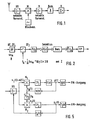
Die heute gebräuchlichen Empfänger für Hörfunk und Fernsehen beruhen auf der Struktur der Überlagerungsempfänger, dessen Blockschaltbild in Fig. 1 dargestellt ist. Das Empfangssignal wird über einen selektiven, in der Mittenfrequenz variierbaren, rauscharmen Vorverstärker einem Mischer zugeführt und auf eine konstante ZF-Frequenz umgesetzt. Danach folgt die eigentliche Selektion und die Demodulation. Dieses Empfängerkonzept erfordert einen sehr frequenzkonstanten Mischoszillator und für die Selektion hochselektive, im Abgleich aufwendige Bandfilter. Das Verfahren war lange Zeit den technologischen Möglichkeiten angepasst und hat inzwischen einen hohen Entwicklungsstand erreicht.The receivers currently used for radio and television are based on the structure of the superimposed receivers, the block diagram of which is shown in FIG. 1. The received signal is fed to a mixer via a selective, low-noise preamplifier that can be varied in the center frequency and converted to a constant IF frequency. This is followed by the actual selection and demodulation. This receiver concept requires a very frequency-constant mixing oscillator and for the selection of highly selective band filters that are complex to adjust. The process was adapted to the technological possibilities for a long time and has now reached a high level of development.
Digitale Systeme zur Signalverarbeitung arbeiten mit quantisierten, digitalisierten Abtastwerten einer Zeitfunktion. Die Form der Abtastimpulse ist dabei von entscheidender Bedeutung hinsichtlich unerwünschter Verzerrungen im Spektrum der abgetasteten Funktion. Im Idealfall handelt es sich bei der Abtastfunktion um eine periodische Folge von Dirac-Impulsen. Das abgetastete Signal lässt sich dann wie folgt angeben![]()
![]()
Die Fouriertransformierte dieses Signals lautet![]()
![]()
Die Abtastfrequenz ist dabei fo=1/To. Aus der Darstellung für die Fouriertransformierte lässt sich entnehmen, dass jede Abtastung eine periodische Wiederholung des Urspektrums bewirkt. Gleichzeitig kann dadurch auch ein Signal in der Frequenzlage umgesetzt werden. Die Abtastfrequenz muss bezüglich der Bandbreite B des abzutastenden Signals die Bedingung![]()
![]()
Bei realer Abtastung mit einem Abtast-Halteglied erhält man eine periodische Wiederholung des mit
An die Präzision der Abtastung und die Grenzfrequenz der beteiligten Komponenten sind deshalb hohe Anforderungen zu stellen. Eine totale Digitalisierung eines Empfängers ist somit wenig sinnvoll.The precision of the scanning and the cutoff frequency of the components involved must therefore meet high requirements. Total digitization of a receiver is therefore not very useful.
Das Blockschaltbild aus Fig. 2 besitzt eine dem Überlagerungsempfänger entsprechende Struktur. Ein breites Empfangsband wird in der H F- oder in der ZF-Ebene mit analogen Filtern vorselektiert. Die anschliessende Abtastung erfordert eine entsprechend der breitbandigen Vorselektion hohe Abtastrate. Mit der Abtastung kann eine gleichzeitige Abwärtsmischung in eine neue ZF- Ebene verbunden werden. Das eigentliche Nutzsignal wird auf digitale Weise selektiert (digitaler Bandpass). Es entfällt damit der schwierige Abgleich herkömmlicher Bandfilter. Die so erreichbare hohe Selektion erfordert, je nach Filtergrad, in Verbindung mit der hohen Bandbreite des nur schwach selektierten Eingangssignals extrem schnelle digitale Bausteine. Das Konzept ist somit den technologischen Gegebenheiten nicht angepasst.The block diagram from FIG. 2 has a structure corresponding to the overlay receiver. A broad reception band is preselected in the HF or IF level with analog filters. The subsequent scanning requires a high scanning rate corresponding to the broadband preselection. Simultaneous downmixing into a new IF level can be combined with the sampling. The actual useful signal is selected digitally (digital band pass). This eliminates the difficult adjustment of conventional bandpass filters. The high selection that can be achieved in this way, depending on the degree of filtering, in connection with the high bandwidth of the poorly selected input signal, requires extremely fast digital components. The concept is therefore not adapted to the technological situation.
Die Demodulation kann z. B. im Fall eines amplitudenmodulierten Signals durch die einfach zu realisierende Betragsbildung und eine nochmalige digitale Tiefpassfilterung erfolgen, wobei die im analogen Fall übliche Methode zur Demodulation digital nachgebildet wird.The demodulation can e.g. B. in the case of an amplitude-modulated signal through the easy-to-implement amount formation and repeated digital low-pass filtering, the analog demodulation method being digitally simulated.
Ausser der hohen Abtastrate und Rechengeschwindigkeit besitzt dieses System weiterhin den Nachteil, dass eine Verstimmung zwischen Trägerfrequenz und Mittenfrequenz des Bandfilters Verzerrungen im demodulierten Signal verursachen - siehe auch nachfolgender Abschnitt.In addition to the high sampling rate and computing speed, this system also has the Disadvantage that a detuning between carrier frequency and center frequency of the bandpass filter causes distortions in the demodulated signal - see also the following section.
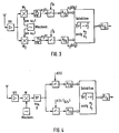
Der asynchrone Empfang mit Demodulation im Basisband (ZF=0) erfordert die gleichzeitige Abwärtsmischung mit Hilfe zweier orthogonaler Signale. Die Struktur dieses Empfängers, in Fig. 3 dargestellt, ist bereits bekannt [3].Asynchronous reception with demodulation in the baseband (IF = 0) requires simultaneous downmixing using two orthogonal signals. The structure of this receiver, shown in Fig. 3, is already known [3].
Das Eingangssignal sei:![]()
![]()
Dann erhält man nach der Multiplikation mit![]()
![]()
![]()
![]()
![]()
![]()
![]()
![]()
Mit Am wird der Fall berücksichtigt, dass die Trägerfrequenz nicht exakt mit der Frequenz des Mischoszillators übereinstimmt. Diese beiden zu den Zeitpunkten k · To abgetasteten Signale können im Digitalteil des Empfängers auf die exakte Signalbandbreite begrenzt werden (Selektion). Bei Frequenzversatz Am werden hier die vom oberen und unteren Seitenband herrührenden Anteile des Signalspektrums jeweils unterschiedlich gefiltert, was im demodulierten Signal nicht mehr rückgängig zu machende Verzerrungen der Amplitude und Phase verursacht. Solange jedoch durch die Filterung, beschrieben durch die Faltung mit der Gewichtsfunktion h(kTo) des Digitalfilters, die beiden Signale u1 und u2 infolge Frequenzversatz noch nicht berührt werden, d.h.


![]()
- Φ(kTo) = Ω(kTo) = Δω - ϕ(kTo) + ϕ1 (kTo)
- Φ (kT o ) = Ω (kT o ) = Δω - ϕ (kT o ) + ϕ 1 (kT o )
Die Momentanphase Φ(kTo) ist durch das Phasenrauschen ϕ1 des Mischoszillators und bei Frequenzversatz durch einen konstant anwachsenden Term verfälscht, welcher u.a. Schwierigkeiten hinsichtlich des begrenzten Wertebereichs verursacht. Die Momentanfrequenz Q wird durch Differenzieren der Momentanphase gewonnen. Sie ist um Δω-ϕ1 verfälscht. Fehlende Synchronität und Phasenrauschen des Mischoszillators werfen also erhebliche Probleme auf.The instantaneous phase Φ (kT o ) is falsified by the phase noise ϕ 1 of the mixing oscillator and, in the event of frequency offset, by a constantly increasing term, which among other things causes difficulties with regard to the limited range of values. The instantaneous frequency Q is obtained by differentiating the instantaneous phase. It is falsified by Δω-ϕ 1 . The lack of synchronism and phase noise of the mixing oscillator therefore pose considerable problems.
Eine weitere Realisierung des asynchronen Hybridempfängers ist in Fig. 4 dargestellt. Es entfällt die Abwärtsmischung mit zwei orthogonalen harmonischen Signalen. Statt dessen wird das Empfangssignal in derZF-Ebenevorselektiert und mit zwei zeitlich (um eine viertel Taktdauer) verschobenen Impulsfolge abgetastet. Die Abtastung bewirkt eine gleichzeitige Abwärtsmischung ins Basisband mit Zwischenfrequenz Null, wenn die Abtastrate![]()
![]()
Am Beispiel von Fig. 5 soll das Prinzip eines Synchronempfängers erläutert werden. Wesentlicher Bestandteil dieses Systems ist eine phasengerastete Regelschleife (phase-locked-loop, PLL), mit welcher ein spannungsgesteuerter Oszillator (voltage-controlled-oscillator, VCO) in Frequenz und Phase mit einem zu empfangenden Signal synchronisiert wird. Mit diesem synchronisierten Signal wird das Empfangssignal unter Umgehung der ZF-Ebene direkt im Basisband herabgemischt und synchron demoduliert. Ein nachfolgender Demodulator wie z.B. beim Überlagerungsempfänger oder beim Empfänger aus Fig. 4 entfällt somit. Durch die Synchrondemodulation ergibt sich ein geringerer Schwellwert.The principle of a synchronous receiver will be explained using the example of FIG. 5. An essential component of this system is a phase-locked loop (PLL), with which a voltage-controlled oscillator (VCO) is synchronized in frequency and phase with a signal to be received. With this synchronized signal, the received signal is bypassed directly in the baseband, bypassing the IF level, and demodulated synchronously. A subsequent demodulator such as the superimposed receiver or the receiver from FIG. 4 is thus omitted. The synchronous demodulation results in a lower threshold value.
Wird das verrauschte Eingangssignal mit
- x1 (t) + n(t) = a1 (t) · sin (ωTt + ϕT) + n(t)
angesetzt, und das VCO-Signal mit
- xo(t) = ao · cos (ωot + ϕo)
wobei die Phase ϕo(t) durch die Beziehung
- ϕo(t) = ko oft y(τ) d
gegeben ist, so erhält man die bekannte Differentialgleichung des PLL[5]:

- x 1 (t) + n (t) = a 1 (t) sin (ω T t + ϕ T ) + n (t)
and the VCO signal with
- x o (t) = a o · cos (ω o t + φ o)
where the phase ϕ o (t) by the relationship
- ϕ o (t) = k oo f t y (τ) d
is given, one obtains the known differential equation of the PLL [5]:
Der PLL besitzt die Eigenschaft, einen gewissen Bereich der Verstimmung Δω selbsttätig auszuregeln (Fangbereich) und den einmal erreichten synchronen Zustand zu bewahren. Im synchronen Zustand Δω=o lässt sich bei kleinem Phasenfehler Φ(t) die Sinus-Funktion durch ihr Argument ersetzen. Aus der damit entstandenen linearen Differentialgleichung kann die Tiefpass-Übertragungsfunktion des linearisierten PLL abgeleitet werden:![]()
![]()
![]()
![]()
Zwischen dem Steuersignal y(t) des VOC und der Phase des Eingangssignals kann unter Berücksichtigung des Rauschens n'(t) der Zusammenhang![]()
![]()
![]()
![]()
![]()
![]()
Wenn die Bandbreite der Übertragungsfunktion H (s) genügend gross gewählt wird, setzt sich das demodulierte Signal y(t) aus einem dem modulierenden Signal v(t) direkt proportionalen Anteil und einem Rauschanteil zusammen. Zur Begrenzung dieses Rauschanteils ist eine ausgangsseitige Bandbegrenzung erforderlich (T, (s)).If the bandwidth of the transfer function H (s) is chosen to be sufficiently large, the demodulated signal y (t) is composed of a component which is directly proportional to the modulating signal v (t) and a noise component. To limit this noise component, an output band limitation is required (T, (s)).
Mit dem um 90° phasenverschobenen VCO-Signal![]()
![]()
![]()
![]()
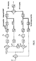
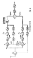
Die Struktur des bekannten direkt mischenden, synchronen Empfängers aus Fig. 5 lässt sich in einen HF-Teil und in einen davon getrennten NF-Teil zerlegen. Das neue Empfangssystem stellt den Hybridenaufbau eines synchronen Homodynempfängers mit dem in Analogtechnik realisierten HF-Teil (Vorverstärker, Mischer, spannungsgesteuerter Oszillator, Phasenschieber) und dem digital realisierten NF-Teil (Schleifenfilter, Ausgangstiefpass, Verstärkungsregelung) dar. Anhand der Fig. 6 soll diese Schaltung erläutert werden.The structure of the known direct-mixing, synchronous receiver from FIG. 5 can be broken down into an HF part and a separate NF part. The new reception system represents the hybrid structure of a synchronous homodyne receiver with the HF part (preamplifier, mixer, voltage-controlled oscillator, phase shifter) and the digitally implemented LF part (loop filter, output low-pass, gain control) implemented in analog technology Circuit will be explained.
Das Eingangssignal wird einem Vorverstärker VV zugeführt. Der Verstärkerausgang spaltet sich in zwei Zweige auf. Der eine in der Figur oben eingezeichnete Zweig besteht aus dem Mischer M1 mit nachgeschaltetem Tiefpass TP, und dem darauffolgenden Baustein für die mit der Abtastfrequenz fA erfolgende Signalabtastung. Der Ausgang der genannten Abtaststufe führt zu einem Analog-Digital-Wandler A/D, dessen Ausgangssignal einem Schleifenfilter F(z) zugeführt wird. Der Ausgang dieses Schleifenfilters führt zu dem zugehörigen Ausgangstiefpass F1 (z) und andererseits über einen Digital-Analog-Wandler D/A zu dem spannungsgesteuerten Oszillator VCO, dessen Ausgangssignal xo(t) dem Mischer M1 zugeführt wird. Gleichzeitig wird das Ausgangssignal des VCO über einen die Phase um π/2 drehenden Phasenschieber Ph geleitet, dessen Ausgangssignal x2(t) den Mischer M2 beaufschlagt.The input signal is fed to a preamplifier VV. The amplifier output splits into two branches. The one shown in the figure above consists of the mixer M 1 with a downstream low pass TP, and the subsequent module for the signal sampling with the sampling frequency f A. The output of the sampling stage leads to an analog-to-digital converter A / D, the output signal of which is fed to a loop filter F (z). The output of this loop filter leads to the associated output low pass F 1 (z) and, on the other hand, via a digital-to-analog converter D / A to the voltage-controlled oscillator VCO, the output signal x o (t) of which is fed to the mixer M 1 . At the same time, the output signal of the VCO is passed via a phase shifter Ph which rotates the phase by π / 2 and whose output signal x 2 (t) acts on the mixer M 2 .
Der andere Zweig auf der Ausgangsseite des Vorverstärkers VV besteht aus einem Mischer M2 und dem Tiefpass TP2. Das durch diesen Tiefpass selektierte Signal führt zu einer Abtaststufe, die das vorhandene Signal mit der Frequenz fA abtastet.The other branch on the output side of the preamplifier VV consists of a mixer M 2 and the low pass TP 2 . The signal selected by this low pass leads to a sampling stage which samples the existing signal with the frequency f A.
Der Ausgang dieser Abtaststufe führt über einen Analog-Digital-Wandler A/D. Sein Ausgangssignal yi(kTo) wird auf einen Ausgangstiefpass F2(z) gegeben. Das zuletzt genannte Signal dient gleichzeitig der Verstärkungsregelung, dargestellt durch die Stufe FR(z), deren Ausgangssignal nach Umwandlung in einen Digital-Analog-Wandler D/A beim dargestellten Ausführungsbeispiel dem Vorverstärker VV zugeführt wird.The output of this sampling stage leads via an analog-digital converter A / D. Its output signal y i (kT o ) is given to an output low pass F 2 (z). The last-mentioned signal also serves to control the gain, represented by the stage F R (z), the output signal of which, after conversion into a digital-to-analog converter D / A, is fed to the preamplifier VV in the exemplary embodiment shown.
Es sei bereits hier darauf hingewiesen, dass dieses Regelsignal auch dem spannungsgesteuerten Oszillator VCO oder den beiden Tiefpässen TP1 und TP2 zugeführt werden kann.It should already be pointed out here that this control signal can also be supplied to the voltage-controlled oscillator VCO or to the two low-pass filters TP 1 and TP 2 .
Aus den an den beiden Ausgangstiefpässen F1 (z) bzw. Fz(z) vorhandenen Signalen kann über einen Schalter S das gewünschte amplituden-oder frequenzmodulierte Signal ausgewählt werden und über einen nachgeschalteten Digital-Analog-Wandler D/A zum analogen NF-Signal zurückverwandelt werden.The desired amplitude- or frequency-modulated signal can be selected from the signals present at the two output low-pass filters F 1 (z) and F z (z) via a switch S and via a downstream digital-to-analog converter D / A to the analogue LF- Signal can be converted back.
Das Systemverhalten dieser linearisierten analog-digitalen (hybriden) phasengerasteten Regelschleife PLL im Empfangssystem gemäss Fig. 6 ist sowohl im Laplace-Bereich als auch unter Verwendung der Z-Transformation darstellbar. Die Bestimmung des optimalen digitalen Schleifenfilters F(z) nach der Optimalfiltertheorie von Wiener zeigt, dass bei Berücksichtigung der durch die Abtastung und die Digital-Wandlung verursachten Zeitverzögerung das optimale digitale Schleifenfilter einen höheren Grad besitzt als im entsprechenden analogen Fall [5].The system behavior of this linearized analog-digital (hybrid) phase locked PLL control loop in the receiving system according to FIG. 6 can be represented both in the Laplace area and using the Z transformation. The determination of the optimal digital loop filter F (z) according to Wiener's optimal filter theory shows that, taking into account the time delay caused by the sampling and digital conversion, the optimal digital loop filter has a higher degree than in the corresponding analog case [5].
Dieses neue Empfängerkonzept nach Fig. 6 kann folgendermassen charakterisiert werden:This new receiver concept according to FIG. 6 can be characterized as follows:
Die Synchrontechnik unter Verwendung einer phasengerasteten Regelschleife gewährleistet eine phasengenaue synchrone Abwärtsmischung des Empfangssignals ins Basisband.The synchronous technology using a phase locked loop ensures a phase-accurate synchronous downmixing of the received signal into the baseband.
Es gibt keine Zwischenfrequenz und somit ergeben sich keine Probleme mit der Spiegelfrequenz (Spiegelfrequenz ist gleich der Empfangsfrequenz).There is no intermediate frequency and therefore there are no problems with the image frequency (image frequency is equal to the reception frequency).
Es ist keine Vorselektion erforderlich. Die Bandbegrenzung erfolgt im Basisband durch die den Mischern M1, M2 folgenden Tiefpässe TP1, TP2. Deren Bandbreite wird durch die Abtastfrequenz bestimmt.No pre-selection is required. The band limitation is performed in the baseband by the mixers M 1, M 2 following low-pass filters TP 1, TP. 2 The bandwidth is determined by the sampling frequency.
Eine weitere Bandbegrenzung wird durch die Übertragungsfunktion der phasengerasteten Regelschleife verursacht.A further band limitation is caused by the transfer function of the phase locked loop.
Das Ausgangssignal des spannungsgesteuerten Oszillators VCO muss sehr arm an Oberwellen sein, um bei fehlender Vorselektion einen Mehrfachempfang zu verhindern.The output signal of the voltage-controlled oscillator VCO must be very low in harmonics in order to prevent multiple reception if there is no preselection.
Die Mischer müssen in einem weiten Dynamikbereich verzerrungsfrei arbeiten [2].The mixers must operate without distortion in a wide dynamic range [2].
Mit der Synchrondemodulation ist ein niedrigerer Schwellwert erreichbar als mit herkömmlichen Demodulatoren.A lower threshold value can be achieved with synchronous demodulation than with conventional demodulators.
Die Analogtechnik ist die einzige zur Verfügung stehende Technologie zum Aufbau der Systemkomponenten, die hochfrequente Signale verarbeiten müssen, wie regelbarer Vorverstärker VV, Mischer, spannungsgesteuerter Oszillator VCO und Phasenschieber Ph. Durch Verlegen der Abtastung ins Basisband entfällt eine H F-seitige selektive Vorfilterung.Analog technology is the only technology available to build up the system components that have to process high-frequency signals, such as a controllable preamplifier VV, mixer, voltage-controlled oscillator VCO and phase shifter Ph. By moving the sampling into the baseband, there is no HF-side selective pre-filtering.
Die digitale Realisierung des Niederfrequenzteils verlangt die spektrale Begrenzung des Eingangssignals vor der Abtastung und eine Analog-Digital-Wandlung. Die dadurch verursachten Phasenfehler müssen bei der Wahl des digitalen Schleifenfilters berücksichtigt werden.The digital realization of the low-frequency part requires the spectral limitation of the input signal before sampling and an analog-to-digital conversion. The phase errors caused by this must be taken into account when choosing the digital loop filter.
Digitale Systeme bleiben in der Anwendung grundsätzlich auf den Niederfrequenzbereich beschränkt. Die Grenzfrequenz erhöht sich aber langsam infolge technologischer Fortschritte, so dass in absehbarer Zeit auch die Verarbeitung des FBAS-Signals beim Fernsehen möglich sein wird. Die digitale Verarbeitung ermöglicht eine vollständige Integration.The use of digital systems is basically limited to the low frequency range. However, the cut-off frequency is slowly increasing as a result of technological advances, so that it will also be possible to process the composite signal on television in the foreseeable future. Digital processing enables full integration.
Die Eigenschaften des digitalen N F-Teils (Filterung, Steuerung) sind programmierbar.The properties of the digital NF part (filtering, control) are programmable.
Bei einer Serienfertigung tauchen keine Toleranzprobleme auf. Abgleicharbeiten entfallen.There are no tolerance problems in series production. Adjustment work is not necessary.
Die Aussteuerbarkeit ist begrenzt. Sie wird durch die Art der Zahlendarstellung und die Anzahl der Quantisierungsstufen bestimmt. Deshalb ist eine Verstärkungsregelung im Analogteil erforderlich.The controllability is limited. It is determined by the type of number representation and the number of quantization levels. Therefore a gain control in the analog section is required.
Die allgemeine Grundschaltung aus Fig. 6 ist sowohl für den Empfang von amplitudenmodulierten Signalen als auch für den Empfang von winkelmodulierten Signalen geeignet. Der in der Grundstruktur enthaltene PLL muss für den jeweiligen Anwendungsfall spezialisiert, d.h. programmiert werden. Im Fall von zweiseitenbandamplitudenmodulierten Signalen mit Träger muss der PLL so schmalbandig ausgelegt werden, dass er nur auf den gegebenenfalls verrauschten Träger synchronisiert (Schmalband-PLL). Das synchrondemodulierte Nutzsignal steht im IN-PHASE-ZWEIG zur Verfügung. Die Selektion erfolgt mit dem Ausgangstiefpass F2(z).The general basic circuit from FIG. 6 is suitable both for the reception of amplitude-modulated signals and for the reception of angle-modulated signals. The PLL contained in the basic structure must be specialized, ie programmed, for the respective application. In the case of double-sideband amplitude-modulated signals with a carrier, the PLL must be designed so narrow-band that it only synchronizes with the noisy carrier (narrow-band PLL). The synchronously demodulated useful signal is available in the IN-PHASE BRANCH. The selection is made with the initial low pass F 2 (z).
Frequenzmodulierte Signale erfordern in der Schaltung gemäss Fig. 6 einen Breitband-PLL. Das Schleifenfilter und die statische Schleifenverstärkung müssen so dimensioniert werden, dass der PLL zum einen den maximalen Frequenzhub ausregeln kann, und andererseits das Nutzsignal in seiner ganzen Bandbreite unverzerrt demoduliert wird. Das Ausgangssignal y(kTo) steht im Quadraturzweig zur Verfügung.Frequency-modulated signals require a broadband PLL in the circuit according to FIG. 6. The loop filter and the static loop gain must be dimensioned so that the PLL can regulate the maximum frequency swing on the one hand, and on the other hand, the useful signal is demodulated in its entire bandwidth without distortion. The output signal y (kT o ) is available in the quadrature branch.
Ein Tiefpass F, (z), dessen Grenzfrequenz gleich der höchsten NF-Frequenz des demodulierten Nutzsignals ist, dient zur Rauschoptimierung.A low-pass filter F, (z), whose cut-off frequency is equal to the highest LF frequency of the demodulated useful signal, is used for noise optimization.
Phasenmodulierte Signale mit geringem Phasenhub werden mit einem Schmalband-PLL demoduliert. Die Grenzfrequenz der Übertragungsfunktion des PLL muss kleiner sein als die kleinste Nutzsignalfrequenz. Das demodulierte Signal wird vor dem Schleifenfilter F(z) abgegriffen.Phase-modulated signals with a small phase shift are demodulated with a narrowband PLL. The limit frequency of the PLL transfer function must be lower than the lowest useful signal frequency. The demodulated signal is tapped before the loop filter F (z).
Amplituden- und 2-PSK-modulierte Signale sind in der Form![]()
![]()
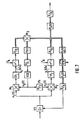
Das auf den Vorverstärker VV eingespeiste Eingangssignal wird am Ausgang des Verstärkers wieder auf zwei Zweige aufgeteilt. Der eine Zweig besteht wie bei der in der Fig. 6 beschriebenen Schaltung aus der Serienschaltung eines Mischers M1, eines Tiefpasses TP1 und einer Abtasteinrichtung v mit nachgeschaltetem Analog-Digital-Wandler A/D. Das Ausgangssignal dieses Wandlers wird nun dem einen Eingang eines weiteren Mischers M3 zugeführt.The input signal fed to the preamplifier VV is again divided into two branches at the output of the amplifier. One branch consists, as in the circuit described in FIG. 6, of the series connection of a mixer M1, a low-pass filter TP 1 and a sampling device v with a downstream analog-digital converter A / D. The output signal of this converter is now fed to one input of a further mixer M 3 .
Der zweite Zweig besteht analog der Schaltung gemäss der Fig. 6 aus der Serienschaltung eines Mischers M2, eines Tiefpasses TPz, einer Abtasteinrichtung fA mit nachgeschaltetem Analog-Digital-Wandler A/D, der zu einem zweiten Eingang des genannten Mischers M3 führt. Der Ausgang des Mischers M3 ist mit dem erforderlichen Schleifenfilter F(z) verbunden, dessen Ausgangssignal einem Digital-Analog-Wandler D/A zugeführt wird, der seinerseits den spannungsgesteuerten Oszillator VCO speist. Der Ausgang des Oszillators VCO führt zum einen mit seinem Ausgangssignal xo direkt zum Mischer M1 und zum anderen über einen die Phase um π/2 drehenden Phasenschieber Ph zum Mischer Mz.Analogous to the circuit according to FIG. 6, the second branch consists of the series connection of a mixer M 2 , a low-pass filter TP z , a scanning device f A with a downstream analog Digital converter A / D, which leads to a second input of said mixer M 3 . The output of the mixer M 3 is connected to the required loop filter F (z), the output signal of which is fed to a digital-to-analog converter D / A, which in turn feeds the voltage-controlled oscillator VCO. The output of the oscillator VCO leads on the one hand with its output signal x o directly to the mixer M 1 and on the other hand via a phase shifter Ph which rotates the phase by π / 2 to the mixer M z .
Der Ausgang des Analog-Digital-Wandlers A/D des zweiten Zweiges ist mit einem Ausgangstiefpass FA(z) verbunden, der seinerseits über einen Digital-Analog-Wandler D/A das gewünschte analoge NF-Signal abgibt.The output of the analog-digital converter A / D of the second branch is connected to an output low-pass filter F A (z), which in turn emits the desired analog LF signal via a digital-analog converter D / A.
Die Regelinformation zur Verstärkungsregelung wird gewonnen, indem das Ausgangssignal y; des zweiten Zweiges nach einer Tiefpassfilterung F2(z) durch eine Betragsbildung B gleichgerichtet wird. Im dargestellten Ausführungsbeispiel führt dieses Signal nach dem Regelfilter FR(z) und dem Digital-Analog-Wandler D/A auf den VorverstärkerVV.The control information for gain control is obtained by output signal y; of the second branch is rectified by a low-pass filtering F 2 (z) by forming an amount B. In the exemplary embodiment shown, this signal leads to the preamplifier VV after the control filter F R (z) and the digital / analog converter D / A.
Die beiden ins Basisband hinabgemischten Quadratursignale sind![]()
![]()
![]()
![]()
Nach einer weiteren Multiplikation und Tiefpassfilterung steht das Signal![]()
![]()
Restseitenbandsignale mit Träger sind in der Form
![]()
![]()
![]()

![]()
![]()
![]()
Der Einfachheit halber werde die Mischerkonstante km=1 gesetzt. Wird nun yq(t) Hilbert-transformiert![]()
![]()
Die hierfür geeignete Schaltung ist in der Fig. 8 dargestellt. Auch hier wird das Eingangssignal nach entsprechender Vorverstärkung in VV auf zwei Zweige aufgeteilt. Der eine beinhaltet die Serienschaltung eines Mischers M1 mit einem Tiefpass TP1, einer Abtastvorrichtung fA und dem nachgeschalteten Analog-Digital-Wandler A/D. Dessen Ausgang führt zu einem breitbandigen Hilbert-Transformator und gleichzeitig über ein Schleifenfilter F(z) und einen Digital-Analog-Wandler D/A auf einen spannungsgesteuerten Oszillator VCO. Dessen Ausgangssignal xo wird zum Mischer M1 und gleichzeitig auf einen die Phase um π/2 drehenden Phasenschieber Ph geführt, dessen Ausgangssignal x1 dem Mischer M2 zugeführt wird. Dieser Mischer Mz bildet den zweiten Zweig zusammen mit dem nachgeschalteten Tiefpass TP2, der Abtasteinrichtung fA, dem darauffolgenden Analog-Digital-Wandler A/D, dessen Ausgangssignal yi(kTo) zusammen mit dem Ausgangssignal Yq einem Addierer A zugeführt, dessen Ausgang mit einem gemeinsamen Ausgangstiefpass FA(z) verbunden ist, der seinerseits zu dem nachgeschalteten Digital-Analog-Wandler D/A führt. An dessen Ausgang ist das gewünschte analoge NF-Signal abgreifbar.The circuit suitable for this is shown in FIG. 8. Here too, the input signal is divided into two branches after appropriate pre-amplification in VV. One includes the series connection of a mixer M 1 with a low pass TP 1 , a scanning device f A and the downstream analog-to-digital converter A / D. Its output leads to a broadband Hilbert transformer and at the same time via a loop filter F (z) and a digital-to-analog converter D / A to a voltage-controlled oscillator VCO. Its output signal x o is fed to the mixer M 1 and at the same time to a phase shifter Ph which rotates the phase by π / 2 and whose output signal x 1 is fed to the mixer M 2 . This mixer M z forms the second branch together with the downstream low-pass filter TP 2 , the sampling device f A , the subsequent analog-digital converter A / D, whose output signal y i (kT o ) together with the output signal Yq is fed to an adder A, whose output is connected to a common output low pass F A (z), which in turn leads to the downstream digital-to-analog converter D / A. The desired analog LF signal can be tapped at its output.
Die erforderliche Verstärkungsregelung wird gebildet durch die zum A/D-Wandler und Addierer A angeschlossene Regelschleife, bestehend aus der Regeleinheit FR(z) mit nachfolgendem Digital-Analog-Wandler D/A. Beim dargestellten Ausführungsbeispiel wird das danach gewonnene Regelsignal dem Vorverstärker VV zugeführt.The required gain control is formed by the control loop connected to the A / D converter and adder A, consisting of the control unit F R (z) with the subsequent digital / analog converter D / A. In the illustrated embodiment, the control signal obtained thereafter is fed to the preamplifier VV.
Wie bereits anhand der Fig. 6 beschrieben, kann das Regelsignal bei der Schaltung gemäss Fig. 7 und auch der Schaltung gemäss Fig. 8 hiervon abweichend entweder dem spannungsgesteuerten Oszillator VCO zugeführt werden oder gleichzeitig den beiden Tiefpässen TP, und TP2.As already described with reference to FIG. 6, the control signal in the circuit in accordance with FIG. 7 and also in the circuit in accordance with FIG. 8 can be supplied either to the voltage-controlled oscillator VCO or to the two low-pass filters TP and TP 2 at the same time.
Die Empfängerstruktur nach Fig. 8 ist in der Lage, Einseitenband- und Restseitenbandsignale (z.B. Fernsehsignal) synchron zu demodulieren. Unter Einbeziehung eines Breitbandphasenschiebers (realer Hilbert-Transformator) mit der Bandbreite des Einseitenbandsignals lässt sich das unerwünschte Seitenband unterdrücken, ohne dass HF-seitig eine Einseitenbandfilterung vorgenommen wird. Algorithmen zur digitalen Hilbert-Transformation sind bekannt [6], erfordern aber je nach Genauigkeit und Verhältnis von oberer zu unterer Grenzfrequenz einen hohen Rechenaufwand.
- 1. Maurer, R.; Hoffmann, M.
- Demodulatorschaltung mit Regelkreis
- Patentanmeldung, AZ. P 28 53 890.1
- Saarbrücken, Nov. 1978
- 2. Maurer, R.; Blum, A.; Hoffmann, M.
- Direktmischendes Empfangssystem
- Patentanmeldung, AZ. P 29 02 952.5
- Saarbrücken, Dez. 1978
- 3. Schaller, W.
- Digitaler Empfänger
- Kolloquiumsvortrag am 25.01.1980 am Lehr-stuhl für Hoch- und Höchstfrequenztechnikder
- Universität des Saarlandes
- 4. Viterbi, A. J.
- Principles of Coherent Communication
- McGraw-Hill, New York 1966
- 5. Gupta, S. C.
- On optimum Digital Phase-Locked Loop
- IEEE Trans. Com. Techn., vol. COM-16,
- pp. 340-344, Apr. 1968
- 6. Herrmann, O.
- Transversalfilter zur Hilbert-Transformation
- A.E.Ü. 23 (1969), 77-84
- 1. Maurer, R .; Hoffmann, M.
- Demodulator circuit with control loop
- Patent application, AZ. P 28 53 890.1
- Saarbrucken, November 1978
- 2. Maurer, R .; Blum, A .; Hoffmann, M.
- Direct mixing reception system
- Patent application, AZ. P 29 02 952.5
- Saarbrucken, Dec. 1978
- 3. Schaller, W.
- Digital receiver
- Colloquium lecture on January 25, 1980 at the chair for high and ultra-high frequency technology
- University of Saarland
- 4. Viterbi, AJ
- Principles of Coherent Communication
- McGraw-Hill, New York 1966
- 5. Gupta, SC
- On optimum digital phase-locked loop
- IEEE Trans. Com. Techn., Vol. COM-16,
- pp. 340-344, Apr. 1968
- 6. Herrmann, O.
- Transversal filter for Hilbert transformation
- AEÜ. 23: 77-84 (1969)
Claims (11)
Priority Applications (1)
| Application Number | Priority Date | Filing Date | Title |
|---|---|---|---|
| AT82102882T ATE9424T1 (en) | 1981-04-07 | 1982-04-05 | RECEPTION SYSTEM. |
Applications Claiming Priority (2)
| Application Number | Priority Date | Filing Date | Title |
|---|---|---|---|
| DE19813114063 DE3114063A1 (en) | 1981-04-07 | 1981-04-07 | RECEPTION SYSTEM |
| DE3114063 | 1981-04-07 |
Publications (2)
| Publication Number | Publication Date |
|---|---|
| EP0062872A1 EP0062872A1 (en) | 1982-10-20 |
| EP0062872B1 true EP0062872B1 (en) | 1984-09-12 |
Family
ID=6129595
Family Applications (1)
| Application Number | Title | Priority Date | Filing Date |
|---|---|---|---|
| EP82102882A Expired EP0062872B1 (en) | 1981-04-07 | 1982-04-05 | Receiving system |
Country Status (6)
| Country | Link |
|---|---|
| US (1) | US4464770A (en) |
| EP (1) | EP0062872B1 (en) |
| JP (1) | JPS585038A (en) |
| AT (1) | ATE9424T1 (en) |
| CA (1) | CA1182535A (en) |
| DE (2) | DE3114063A1 (en) |
Cited By (3)
| Publication number | Priority date | Publication date | Assignee | Title |
|---|---|---|---|---|
| DE3823552A1 (en) * | 1988-07-12 | 1990-01-18 | Blaupunkt Werke Gmbh | CIRCUIT ARRANGEMENT FOR DEMODULATING AN AUXILIARY CARRIER |
| DE4192400C2 (en) * | 1990-09-28 | 1995-06-14 | Motorola Inc | Demodulation method and device |
| DE4417723A1 (en) * | 1994-05-20 | 1995-11-23 | Ant Nachrichtentech | Device for processing a modulated real-valued analog television signal |
Families Citing this family (50)
| Publication number | Priority date | Publication date | Assignee | Title |
|---|---|---|---|---|
| GB2106734B (en) * | 1981-09-15 | 1986-01-15 | Standard Telephones Cables Ltd | Radio receiver |
| DE3240565C2 (en) * | 1982-11-03 | 1985-12-12 | Telefunken electronic GmbH, 6000 Frankfurt | Direct mixing synchronous receiver |
| US4633399A (en) * | 1984-03-05 | 1986-12-30 | Conoco Inc. | Method of seismic data enhancement using a phase of rectified trace seismic parameter |
| DE3412508A1 (en) * | 1984-04-03 | 1985-10-10 | Industronic, Industrie-Electronic Gmbh & Co Kg, 6980 Wertheim | DEVICE FOR TRANSMITTING ELECTRICAL SIGNALS, ESPECIALLY IN THE LONG-WAVE AREA |
| US4571550A (en) * | 1984-06-22 | 1986-02-18 | Rockwell International Corporation | QAM Demodulator carrier recovery loop using n-m LSB's |
| US4574244A (en) * | 1984-06-22 | 1986-03-04 | Rockwell International Corporation | QAM Demodulator automatic quadrature loop using n-m LSB's |
| DE3505950A1 (en) * | 1985-02-21 | 1986-08-21 | Deutsche Itt Industries Gmbh, 7800 Freiburg | INTEGRATED CIRCUIT FOR IDENTIFYING A PILOT TONE |
| GB2172159A (en) * | 1985-03-07 | 1986-09-10 | Stc Plc | A/d converters |
| US4893316A (en) * | 1985-04-04 | 1990-01-09 | Motorola, Inc. | Digital radio frequency receiver |
| GB2176356A (en) * | 1985-06-12 | 1986-12-17 | Philips Electronic Associated | Method of, and demodulator for, digitally demodulating an ssb signal |
| AU591181B2 (en) * | 1985-09-03 | 1989-11-30 | Motorola, Inc. | Digital radio frequency receiver |
| EP0255553B1 (en) * | 1986-08-07 | 1992-07-22 | Deutsche ITT Industries GmbH | Method for receiving frequency-modulated stereo-multiplex signals |
| CH671856A5 (en) * | 1986-09-05 | 1989-09-29 | Ascom Radiocom Ag | |
| EP0282607B1 (en) * | 1987-03-14 | 1990-08-16 | Deutsche ITT Industries GmbH | Frequency-converter for television signal |
| US5016019A (en) * | 1987-06-05 | 1991-05-14 | The Secretary Of State For Defence In Her Britannic Majesty's Government Of The United Kingdom Of Great Britain And Northern Ireland | Method and apparatus for processing synthetic aperture aerial signals |
| US5398002A (en) * | 1989-02-15 | 1995-03-14 | Samsung Electronics Co., Ltd. | Automatic frequency control system by quadrature-phase in frequency or phase demodulating system |
| EP0413311A3 (en) * | 1989-08-16 | 1991-10-30 | Hitachi, Ltd. | A radio receiver and a radio receiver using a direct conversion |
| US5003621A (en) * | 1989-11-02 | 1991-03-26 | Motorola, Inc. | Direct conversion FM receiver |
| US4979230A (en) * | 1989-12-04 | 1990-12-18 | General Instrument Corporation | Up-conversion homodyne receiver for cable television converter with frequency offset to avoid adjacent channel interference |
| US5028885A (en) * | 1990-08-30 | 1991-07-02 | Motorola, Inc. | Phase-locked loop signal generation system with control maintenance |
| US5222144A (en) * | 1991-10-28 | 1993-06-22 | Ford Motor Company | Digital quadrature radio receiver with two-step processing |
| DE4417725A1 (en) * | 1994-05-20 | 1995-11-23 | Ant Nachrichtentech | Device for digitally demodulating the picture and sound components of a television signal |
| DE4417724A1 (en) * | 1994-05-20 | 1995-11-23 | Ant Nachrichtentech | Device for digitally demodulating the picture and sound components of a television signal |
| CN1082301C (en) * | 1994-09-10 | 2002-04-03 | 三星电子株式会社 | Digital radio transmission-reception apparatus |
| EP0729230B1 (en) * | 1995-02-21 | 2002-10-02 | Tait Electronics Limited | Zero intermediate frequency receiver |
| FR2734681B1 (en) * | 1995-05-23 | 1997-07-04 | Thomson Multimedia Sa | PROCESS FOR DIGITIZING AN INTERMEDIATE FREQUENCY SIGNAL IF, IN PARTICULAR TELEVISION, AND CIRCUIT FOR IMPLEMENTING THIS PROCEDURE |
| FR2735316B1 (en) * | 1995-06-12 | 1997-07-18 | Thomson Multimedia Sa | METHOD FOR DIGITIZING FI VIDEO SIGNALS AND DEVICE FOR CARRYING OUT SAID METHOD |
| US5828955A (en) * | 1995-08-30 | 1998-10-27 | Rockwell Semiconductor Systems, Inc. | Near direct conversion receiver and method for equalizing amplitude and phase therein |
| US6633550B1 (en) * | 1997-02-20 | 2003-10-14 | Telefonaktiebolaget Lm Ericsson (Publ) | Radio transceiver on a chip |
| US6356736B2 (en) * | 1997-02-28 | 2002-03-12 | Maxim Integrated Products, Inc. | Direct-conversion tuner integrated circuit for direct broadcast satellite television |
| US6031878A (en) * | 1997-02-28 | 2000-02-29 | Maxim Integrated Products, Inc. | Direct-conversion tuner integrated circuit for direct broadcast satellite television |
| US5929748A (en) * | 1997-06-12 | 1999-07-27 | Microsoft Corporation | Automated home control using existing electrical lines as a communications medium |
| CA2256779A1 (en) * | 1998-12-21 | 2000-06-21 | Tet Hin Yeap | High speed analog-to-digital converter and digital-to-analog converter |
| US6823133B1 (en) | 1999-11-15 | 2004-11-23 | Lexmark International, Inc. | Apparatus and method for electronic control of DC motor using an all-digital phase-locked loop |
| US6377843B1 (en) * | 2000-03-03 | 2002-04-23 | Paceart Associates, L.P. | Transtelephonic monitoring of multi-channel ECG waveforms |
| JP4063563B2 (en) * | 2002-03-25 | 2008-03-19 | 株式会社日立国際電気 | Direct detection circuit |
| US7072424B2 (en) * | 2002-04-23 | 2006-07-04 | Kyocera Wireless Corp. | Adaptive direct conversion receiver |
| US20040149491A1 (en) * | 2003-01-30 | 2004-08-05 | Fling Richard William | Device and method for improved data transfer |
| US7425995B2 (en) * | 2003-02-28 | 2008-09-16 | Silicon Laboratories, Inc. | Tuner using a direct digital frequency synthesizer, television receiver using such a tuner, and method therefor |
| US7447493B2 (en) * | 2003-02-28 | 2008-11-04 | Silicon Laboratories, Inc. | Tuner suitable for integration and method for tuning a radio frequency signal |
| US7358885B2 (en) | 2003-02-28 | 2008-04-15 | Silicon Laboratories, Inc. | Mixing DAC architectures for a radio frequency receiver |
| WO2004079924A2 (en) * | 2003-02-28 | 2004-09-16 | Silicon Laboratories Inc. | Tuner for radio frequency receivers and associated method |
| US7676210B2 (en) * | 2003-09-29 | 2010-03-09 | Tod Paulus | Method for performing dual mode image rejection calibration in a receiver |
| US7272375B2 (en) | 2004-06-30 | 2007-09-18 | Silicon Laboratories Inc. | Integrated low-IF terrestrial audio broadcast receiver and associated method |
| US7773968B2 (en) * | 2006-11-30 | 2010-08-10 | Silicon Laboratories, Inc. | Interface/synchronization circuits for radio frequency receivers with mixing DAC architectures |
| US20080180579A1 (en) * | 2007-01-31 | 2008-07-31 | Silicon Laboratories, Inc. | Techniques for Improving Harmonic and Image Rejection Performance of an RF Receiver Mixing DAC |
| US7599676B2 (en) * | 2007-01-31 | 2009-10-06 | Silicon Laboratories, Inc. | Power consumption reduction techniques for an RF receiver implementing a mixing DAC architecture |
| US20080181340A1 (en) * | 2007-01-31 | 2008-07-31 | Silicon Laboratories, Inc. | Spur Rejection Techniques for an RF Receiver |
| US20080181337A1 (en) * | 2007-01-31 | 2008-07-31 | Silicon Laboratories, Inc. | Spur and Distortion Management Techniques for an RF Receiver |
| DE102010041571B4 (en) * | 2010-09-28 | 2012-11-22 | Hauni Maschinenbau Ag | Apparatus and method for processing and measuring properties of a moving strand of material |
Family Cites Families (8)
| Publication number | Priority date | Publication date | Assignee | Title |
|---|---|---|---|---|
| US3181122A (en) * | 1961-10-02 | 1965-04-27 | Electro Mechanical Res Inc | Phase code detecting systems having phase-locked loops |
| US3701948A (en) * | 1970-09-17 | 1972-10-31 | North American Rockwell | System for phase locking on a virtual carrier |
| US3669511A (en) * | 1970-09-17 | 1972-06-13 | North American Rockwell | System for phase locking on a virtual carrier received by an asymmetrical receiver |
| US3675131A (en) * | 1971-01-15 | 1972-07-04 | Ibm | Coherent single sideband phase locking technique |
| US3818347A (en) * | 1972-10-10 | 1974-06-18 | Intertel Inc | Receiver for amplitude modulated quadrature carrier signals |
| FR2368184A1 (en) * | 1976-10-18 | 1978-05-12 | Ibm France | CARRIER SYNCHRONIZATION SYSTEM FOR COHERENT PHASE DEMODULATOR |
| DE2902952C2 (en) * | 1979-01-26 | 1986-10-09 | ANT Nachrichtentechnik GmbH, 7150 Backnang | Direct mixing receiving system |
| DE2913172B2 (en) * | 1979-04-02 | 1981-06-11 | Siemens AG, 1000 Berlin und 8000 München | Receiver for high-frequency electromagnetic oscillations with frequency readjustment |
-
1981
- 1981-04-07 DE DE19813114063 patent/DE3114063A1/en not_active Withdrawn
-
1982
- 1982-04-05 AT AT82102882T patent/ATE9424T1/en not_active IP Right Cessation
- 1982-04-05 EP EP82102882A patent/EP0062872B1/en not_active Expired
- 1982-04-05 DE DE8282102882T patent/DE3260702D1/en not_active Expired
- 1982-04-06 JP JP57056149A patent/JPS585038A/en active Pending
- 1982-04-06 CA CA000400564A patent/CA1182535A/en not_active Expired
- 1982-04-07 US US06/366,393 patent/US4464770A/en not_active Expired - Fee Related
Cited By (3)
| Publication number | Priority date | Publication date | Assignee | Title |
|---|---|---|---|---|
| DE3823552A1 (en) * | 1988-07-12 | 1990-01-18 | Blaupunkt Werke Gmbh | CIRCUIT ARRANGEMENT FOR DEMODULATING AN AUXILIARY CARRIER |
| DE4192400C2 (en) * | 1990-09-28 | 1995-06-14 | Motorola Inc | Demodulation method and device |
| DE4417723A1 (en) * | 1994-05-20 | 1995-11-23 | Ant Nachrichtentech | Device for processing a modulated real-valued analog television signal |
Also Published As
| Publication number | Publication date |
|---|---|
| ATE9424T1 (en) | 1984-09-15 |
| CA1182535A (en) | 1985-02-12 |
| US4464770A (en) | 1984-08-07 |
| DE3114063A1 (en) | 1982-10-21 |
| DE3260702D1 (en) | 1984-10-18 |
| JPS585038A (en) | 1983-01-12 |
| EP0062872A1 (en) | 1982-10-20 |
Similar Documents
| Publication | Publication Date | Title |
|---|---|---|
| EP0062872B1 (en) | Receiving system | |
| DE69533246T2 (en) | Method and device for automatic frequency control | |
| DE2902952C2 (en) | Direct mixing receiving system | |
| DE4236087A1 (en) | Tunable antenna system with controllable reactive circuit element - has level detector circuit producing signal which contains component at second harmonic frequency of dither signal | |
| EP0080014A2 (en) | Digital demodulator for frequency-modulated signals | |
| EP0084876A2 (en) | Demodulator arrangement for signals which are frequency-modulated on a carrier wave | |
| EP0308520B1 (en) | Digital-demodulator | |
| EP0334108B1 (en) | Receiver for spread-spectrum signals, especially a GPS-type receiver | |
| DE2164796C3 (en) | Phase control for single sideband receivers | |
| DE2656924C3 (en) | Phase discriminator in a receiver of a data transmission system | |
| EP1993212B1 (en) | Converter | |
| DD292788A5 (en) | METHOD AND DEVICE FOR AUTOMATIC FREQUENCY CONTROL | |
| DE2354718C3 (en) | Demodulation method for phase-shift keyed oscillations and circuit arrangement for carrying out the method | |
| DE2712474C3 (en) | Demodulation system for a multi-phase and multi-stage superposition-modulated carrier wave | |
| DE1591408C2 (en) | Device for receiving several input signals of the same frequency | |
| DE3733967C2 (en) | ||
| DE3938643C2 (en) | Method for reconstructing separated direct-current useful components of IF signals in a direct conversion receiver and receiver for carrying out the method | |
| DE3146280C2 (en) | ||
| EP0602394B1 (en) | Method and device for the correction of phase and amplitude errors for direct conversion receiving devices | |
| EP1643633A1 (en) | Circuit with suppression of unwanted signals , and method | |
| DE3718103C2 (en) | ||
| DE19523433C2 (en) | Circuit arrangement for frequency conversion | |
| EP0351404B1 (en) | Process for timing synchronization | |
| DE2033017B2 (en) | DEVICE FOR RECEIVING MULTIPLE INPUT SIGNALS OF THE SAME FREQUENCY | |
| DE69233486T2 (en) | PSK demodulator with frequency multiplication for phase and frequency correction |
Legal Events
| Date | Code | Title | Description |
|---|---|---|---|
| PUAI | Public reference made under article 153(3) epc to a published international application that has entered the european phase |
Free format text: ORIGINAL CODE: 0009012 |
|
| AK | Designated contracting states |
Designated state(s): AT CH DE FR GB IT LI NL |
|
| 17P | Request for examination filed |
Effective date: 19830209 |
|
| RAP1 | Party data changed (applicant data changed or rights of an application transferred) |
Owner name: AEG - TELEFUNKEN NACHRICHTENTECHNIK GMBH |
|
| KL | Correction list |
Free format text: 83/03 BESCHREIBUNG |
|
| RAP1 | Party data changed (applicant data changed or rights of an application transferred) |
Owner name: ANT NACHRICHTENTECHNIK GMBH |
|
| ITF | It: translation for a ep patent filed |
Owner name: BARZANO' E ZANARDO MILANO S.P.A. |
|
| GRAA | (expected) grant |
Free format text: ORIGINAL CODE: 0009210 |
|
| AK | Designated contracting states |
Designated state(s): AT CH DE FR GB IT LI NL |
|
| REF | Corresponds to: |
Ref document number: 9424 Country of ref document: AT Date of ref document: 19840915 Kind code of ref document: T |
|
| REF | Corresponds to: |
Ref document number: 3260702 Country of ref document: DE Date of ref document: 19841018 |
|
| ET | Fr: translation filed | ||
| PLBE | No opposition filed within time limit |
Free format text: ORIGINAL CODE: 0009261 |
|
| STAA | Information on the status of an ep patent application or granted ep patent |
Free format text: STATUS: NO OPPOSITION FILED WITHIN TIME LIMIT |
|
| 26N | No opposition filed | ||
| ITTA | It: last paid annual fee | ||
| PGFP | Annual fee paid to national office [announced via postgrant information from national office to epo] |
Ref country code: GB Payment date: 19930325 Year of fee payment: 12 |
|
| PG25 | Lapsed in a contracting state [announced via postgrant information from national office to epo] |
Ref country code: GB Effective date: 19940405 |
|
| PGFP | Annual fee paid to national office [announced via postgrant information from national office to epo] |
Ref country code: DE Payment date: 19940614 Year of fee payment: 13 |
|
| GBPC | Gb: european patent ceased through non-payment of renewal fee |
Effective date: 19940405 |
|
| PGFP | Annual fee paid to national office [announced via postgrant information from national office to epo] |
Ref country code: FR Payment date: 19950413 Year of fee payment: 14 |
|
| PGFP | Annual fee paid to national office [announced via postgrant information from national office to epo] |
Ref country code: AT Payment date: 19950426 Year of fee payment: 14 |
|
| PGFP | Annual fee paid to national office [announced via postgrant information from national office to epo] |
Ref country code: NL Payment date: 19950430 Year of fee payment: 14 |
|
| PGFP | Annual fee paid to national office [announced via postgrant information from national office to epo] |
Ref country code: CH Payment date: 19950518 Year of fee payment: 14 |
|
| PG25 | Lapsed in a contracting state [announced via postgrant information from national office to epo] |
Ref country code: DE Effective date: 19960201 |
|
| PG25 | Lapsed in a contracting state [announced via postgrant information from national office to epo] |
Ref country code: AT Effective date: 19960405 |
|
| PG25 | Lapsed in a contracting state [announced via postgrant information from national office to epo] |
Ref country code: LI Effective date: 19960430 Ref country code: CH Effective date: 19960430 |
|
| PG25 | Lapsed in a contracting state [announced via postgrant information from national office to epo] |
Ref country code: NL Effective date: 19961101 |
|
| REG | Reference to a national code |
Ref country code: CH Ref legal event code: PL |
|
| PG25 | Lapsed in a contracting state [announced via postgrant information from national office to epo] |
Ref country code: FR Effective date: 19961227 |
|
| NLV4 | Nl: lapsed or anulled due to non-payment of the annual fee |
Effective date: 19961101 |
|
| REG | Reference to a national code |
Ref country code: FR Ref legal event code: ST |