EP0062871B1 - Load management terminal - Google Patents
Load management terminal Download PDFInfo
- Publication number
- EP0062871B1 EP0062871B1 EP82102879A EP82102879A EP0062871B1 EP 0062871 B1 EP0062871 B1 EP 0062871B1 EP 82102879 A EP82102879 A EP 82102879A EP 82102879 A EP82102879 A EP 82102879A EP 0062871 B1 EP0062871 B1 EP 0062871B1
- Authority
- EP
- European Patent Office
- Prior art keywords
- reset
- microprocessor
- signal
- timer
- load management
- Prior art date
- Legal status (The legal status is an assumption and is not a legal conclusion. Google has not performed a legal analysis and makes no representation as to the accuracy of the status listed.)
- Expired
Links
Images


Classifications
-
- H—ELECTRICITY
- H04—ELECTRIC COMMUNICATION TECHNIQUE
- H04B—TRANSMISSION
- H04B3/00—Line transmission systems
- H04B3/54—Systems for transmission via power distribution lines
-
- G—PHYSICS
- G06—COMPUTING; CALCULATING OR COUNTING
- G06F—ELECTRIC DIGITAL DATA PROCESSING
- G06F11/00—Error detection; Error correction; Monitoring
-
- H—ELECTRICITY
- H02—GENERATION; CONVERSION OR DISTRIBUTION OF ELECTRIC POWER
- H02J—CIRCUIT ARRANGEMENTS OR SYSTEMS FOR SUPPLYING OR DISTRIBUTING ELECTRIC POWER; SYSTEMS FOR STORING ELECTRIC ENERGY
- H02J13/00—Circuit arrangements for providing remote indication of network conditions, e.g. an instantaneous record of the open or closed condition of each circuitbreaker in the network; Circuit arrangements for providing remote control of switching means in a power distribution network, e.g. switching in and out of current consumers by using a pulse code signal carried by the network
- H02J13/00006—Circuit arrangements for providing remote indication of network conditions, e.g. an instantaneous record of the open or closed condition of each circuitbreaker in the network; Circuit arrangements for providing remote control of switching means in a power distribution network, e.g. switching in and out of current consumers by using a pulse code signal carried by the network characterised by information or instructions transport means between the monitoring, controlling or managing units and monitored, controlled or operated power network element or electrical equipment
- H02J13/00007—Circuit arrangements for providing remote indication of network conditions, e.g. an instantaneous record of the open or closed condition of each circuitbreaker in the network; Circuit arrangements for providing remote control of switching means in a power distribution network, e.g. switching in and out of current consumers by using a pulse code signal carried by the network characterised by information or instructions transport means between the monitoring, controlling or managing units and monitored, controlled or operated power network element or electrical equipment using the power network as support for the transmission
- H02J13/00009—Circuit arrangements for providing remote indication of network conditions, e.g. an instantaneous record of the open or closed condition of each circuitbreaker in the network; Circuit arrangements for providing remote control of switching means in a power distribution network, e.g. switching in and out of current consumers by using a pulse code signal carried by the network characterised by information or instructions transport means between the monitoring, controlling or managing units and monitored, controlled or operated power network element or electrical equipment using the power network as support for the transmission using pulsed signals
-
- H—ELECTRICITY
- H04—ELECTRIC COMMUNICATION TECHNIQUE
- H04B—TRANSMISSION
- H04B2203/00—Indexing scheme relating to line transmission systems
- H04B2203/54—Aspects of powerline communications not already covered by H04B3/54 and its subgroups
- H04B2203/5429—Applications for powerline communications
- H04B2203/5458—Monitor sensor; Alarm systems
-
- Y—GENERAL TAGGING OF NEW TECHNOLOGICAL DEVELOPMENTS; GENERAL TAGGING OF CROSS-SECTIONAL TECHNOLOGIES SPANNING OVER SEVERAL SECTIONS OF THE IPC; TECHNICAL SUBJECTS COVERED BY FORMER USPC CROSS-REFERENCE ART COLLECTIONS [XRACs] AND DIGESTS
- Y02—TECHNOLOGIES OR APPLICATIONS FOR MITIGATION OR ADAPTATION AGAINST CLIMATE CHANGE
- Y02E—REDUCTION OF GREENHOUSE GAS [GHG] EMISSIONS, RELATED TO ENERGY GENERATION, TRANSMISSION OR DISTRIBUTION
- Y02E60/00—Enabling technologies; Technologies with a potential or indirect contribution to GHG emissions mitigation
-
- Y—GENERAL TAGGING OF NEW TECHNOLOGICAL DEVELOPMENTS; GENERAL TAGGING OF CROSS-SECTIONAL TECHNOLOGIES SPANNING OVER SEVERAL SECTIONS OF THE IPC; TECHNICAL SUBJECTS COVERED BY FORMER USPC CROSS-REFERENCE ART COLLECTIONS [XRACs] AND DIGESTS
- Y04—INFORMATION OR COMMUNICATION TECHNOLOGIES HAVING AN IMPACT ON OTHER TECHNOLOGY AREAS
- Y04S—SYSTEMS INTEGRATING TECHNOLOGIES RELATED TO POWER NETWORK OPERATION, COMMUNICATION OR INFORMATION TECHNOLOGIES FOR IMPROVING THE ELECTRICAL POWER GENERATION, TRANSMISSION, DISTRIBUTION, MANAGEMENT OR USAGE, i.e. SMART GRIDS
- Y04S40/00—Systems for electrical power generation, transmission, distribution or end-user application management characterised by the use of communication or information technologies, or communication or information technology specific aspects supporting them
- Y04S40/12—Systems for electrical power generation, transmission, distribution or end-user application management characterised by the use of communication or information technologies, or communication or information technology specific aspects supporting them characterised by data transport means between the monitoring, controlling or managing units and monitored, controlled or operated electrical equipment
- Y04S40/121—Systems for electrical power generation, transmission, distribution or end-user application management characterised by the use of communication or information technologies, or communication or information technology specific aspects supporting them characterised by data transport means between the monitoring, controlling or managing units and monitored, controlled or operated electrical equipment using the power network as support for the transmission
Definitions
- This invention relates to a load management terminal according to claim 1.
- ⁇ Several types of distribution network communication systems exist for communicating over the power-line conductors of a utility's power distribution network.
- the purpose of the communication system is to allow a central control station to communicate with individual or groups of utility customers.
- Such communications may include instructions for data acquisition or load control.
- the utility customer location In order to receive and implement these instructions the utility customer location must be equipped with some type of equipment responsive to the received instructions, such as a load management terminal.
- a typical load management terminal is capable of receiving communication signals, determining which of the received signals were addressed to it, and taking appropriate action in response. Appropriate action may be to interrogate a time of day meter, shed specific loads or update a local clock.
- the load management terminal is also capable of transmitting meter data and other information from the customer location, through the distribution network, back to the electric utility.
- load management terminals are typically designed around a microprocessor.
- the microprocessor can perform a variety of functions such as comparing the address of a received signal to stored addresses, performing an error check on the received signal, etc.,'while discrete circuits and output devices, under microprocessor control, perform other necessary functions such as receiving or transmitting a communication signal, disconnecting loads, ets.
- the microprocessor based load management terminal is dependent upon the proper operation of the microprocessor in order to function without problems.
- a microprocessor requires a set of commands, or instructions, in order to perform its intended function, It is possible for a microprocessor to become lost and to begin to execute instructions out of sequence, or to execute phantom instructions, as a result of electrical noise, system transients or the like. When the microprocessor becomes lost it must be reset, or directed to a specific instruction within a program, in order to return to a proper state of operation.
- the chief object of the present invention is to provide a load management terminal control logic circuit to obviate the above-mentioned problems and provide improved operating reliability.
- the invention resides in a load management terminal, control logic curcuit for producing system control signals in a power distribution system, said control logic circuit comprising: memory means containing preprogrammed instructions; a microprocessor producing a diagnostic signal, said diagnostic signal being in a low state in response to one of said instructions and being in a high state in response to another of said instructions, said microprocessor also producing said system control signals; a first timer responsive to said low state of said diagnostic signal, said first timer producing a first reset signal when the time during which said diagnostic signal is in said low state exceeds a predetermined time, said first reset signal input to said microprocessor to effect a reset thereof; and a second timer responsive to said high state of said diagnostic signal, said second timer producing a second reset signal when the time during which said diagnostic signal is in said high state exceeds a predetermined time, said second reset signal input to said microprocessor to effect a reset thereof, said first and second timers comprising the reset circuit.
- the present disclosure reveals a load management terminal having improved reliability and performing an additional load control function.
- the load management terminal is utilized as an end device in a utility's distribution network communication system.
- the distribution network carries electrical power as well as communication signals.
- the load management terminal is comprised of a power-line coupling unit for connecting the load management terminal to the power distribution network.
- a signal receiver and conditioning unit produces a command signal in response to the power-line coupling unit.
- a solid state memory contains preprogrammed data and instructions.
- a microprocessor performs load management functions in response to the command signal.
- the microprocessor additionally produces a diagnostic signal being in a low state in response to one of the instructions and being in a high state in response to another of the instructions.
- a reset circuit is comprised of a first timer responsive to the low state of the diagnostic signal and a second timer responsive to the high state of the diagnostic signal.
- the first and second timers cooperate to monitor the microprocessor and to reset the microprocessor whenever it becomes lost.
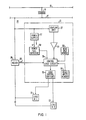
- Fig. '1 is a block diagram illustrating a load management terminal (hereinafter LMT) 13 constructed according to the teachings of the present invention.
- Fig. 1 also illustrates in block diagram form the typical environment in which the LMT 13 is found.
- a primary feeder 15 of a utility's power distribution network is connected to a conductor 17 through a distribution transformer 19.
- the conductor 17 is used to deliver electrical power to a plurality of customer sites, a typical customer site 20 being illustrated in Fig. 1.
- Electrical power is delivered to a plurality of loads 21 and 23 within the customer site 20.
- the electrical power is delivered through an electric energy meter 25 of the type having an encoding register and being capable of producing a pulse signal 26 representative of the electric energy consumption.
- the loads 21 and 23 together with the electric energy meter 25 and the LMT 13 make up the customer site 20.
- the LMT 13 is comprised of a power-line coupling unit 27 which connects the LMT to the power distribution system.
- a signal receiver and conditioner 29 is responsive to the coupling unit 27 to provide command signals in response to received communication signals.
- the command signals are input to a control logic circuit 31.
- the control logic circuit 31 is comprised of several components including a microprocessor and a reset circuit which are described in further detail in conjunction with Fig. 2 hereinbelow.
- a read only memory 32 contains programmed information and instructions necessary for the proper operation of the LMT 13.
- a read/write memory 33 contains meter readings, time of day information, scratch pad calculations and the like.
- the control logic circuit 31 controls a plurality of load control switches 35.
- the control logic circuit 31 also receives the pulse signal 26.
- the control logic circuit 31 provides a plurality of functions such as interrogating the electric energy meter 25 and opening and closing load control switches 35 thereby removing and adding loads to the power distribution network in response to appropriate command signals.
- the LMT 13 additionally includes a power supply 37 producing regulated supply voltages for the LMT.
- One of the supply voltages V is monitored by power fail detector 59.
- a reset signal produced by the power fail detector 59 is input to the control logic circuit 31.
- the power fail detector 59 is discussed in further detail in conjunction with Figs. 2 and 4.
- Fig. 2 a block diagram illustrating the microprocessor 41 and the reset circuit 43 of the control logic circuit 31 is shown.
- the microprocessor 41 produces a diagnostic signal 45 in response to preprogrammed instructions.
- the diagnostic signal 45 is input to both a low timer 47 and a high timer 49.
- the low timer 47 produces a first reset signal 50 which is input to a NAND gate 53.
- the high timer 49 produces a second reset signal 51 which is also input to the NAND gate 53.
- An output signal of the NAND gate 53 is input to a NOR gate 55.
- An output signal of the NOR gate 55 is input to an interrupt request input terminal IRQ of the microprocessor 41.
- the output signal of the NOR gate 55 is also input to a reset timer 57.
- FIG. 2 illustrates the power fail detector 59 which produces a third reset signal 60 in response to the regulated supply voltage V.
- the third reset signal 60 is input to the NOR gate 55.
- the operation of the reset circuit 43 shown in Fig. 2 may be more easily understood by referring to Fig. 3 wherein a detailed timing diagram of the diagnostic signal 45 is illustrated.
- the microprocessor 41 inhibits both the low timer 47 and the high timer 49 from operating.
- the microprocessor 41 executes an initialization routine wherein one of the early instructions is to set the diagnostic signal in high state.
- One of the last instructions of the initialization routine instructs the microprocessor to set the diagnostic signal to the low state as shown at time T 2 .
- the diagnostic signal is in the low state.
- the normal operating routine begins and the microprocessor is instructed to set the diagnostic signal in the high state.
- the diagnostic signal remains in the high state until the end of the normal operating routine when it is again set to the low state as shown at time T 4 .
- a pattern is developed wherein the diagnostic signal 45 spends a predetermined time in the high state and a predetermined time in the low state.
- the low time 47 is responsive to the time during which the diagnostic signal 45 is in the low state. As shown in Fig. 3, the time the diagnostic signal 45 is in the low state should not exceed the time period between time T 4 and time T s , for example. If the time during which the diagnostic signal 45 exceeds this predetermined time period the assumption is that the microprocessor 41 is lost and must be reset. The low timer 47 produces the first reset signal 50 in response to this condition.
- the high timer 49 is responsive to the time during which the diagnostic signal 45 is in the high state.
- the time during which the diagnostic signal 45 is in the high state should not exceed the time period between time T 3 and time T 4 , for example. If the diagnostic signal 45 remains in the high state beyond this predetermined time period the assumption again is that the microprocessor 41 is lost and must be reset.
- the high timer 49 produces the second reset signal in response to this condition.
- the first and second reset signals 50 and 51 propagate through the gates 53 and 55 to the interrupt request input terminal IRQ of the microprocessor 41 and the reset timer 57.
- the microprocessor 41 Upon receipt of one of the reset signals at the interrupt request input terminal IRQ the microprocessor 41 performs an interrupt subroutine for protecting the read/write memory 33.
- the reset timer 57 delays the reset signals so as to allow enough time for the microprocessor 41 to complete the interrupt subroutine before the microprocessor is reset.
- the power failure detector 59 produces the third reset signal 60 whenever the supply voltage V falls below a predetermined voltage level.
- the third reset signal 60 propagates through the gate 55 to initiate the interrupt subroutine in a similar fashion to the first and second reset signals 50 and 51, respectively.
- the third reset signal 60 is delayed by the reset timer 57 such that the interrupt subroutine is completed.
- the third reset signal 60 will hold the microprocessor 41 in the reset condition until the supply voltages return to acceptable levels.
- Fig. 4 is an electrical schematic illustrating the circuit details of the components shown in Fig. 2.
- the microprocessor 41 produces the diagnostic signal 45 which is input to an inverter 62.
- An output terminal of the inverter 62 is connected to an inputterminal of a Schmitt trigger 64through a diode 65.
- the input terminal of the Schmitt trigger 64 is connected to a positive voltage source through a resistor 66, to ground through a capacitor 67 and to the reset terminal R of the microprocessor 41 through a diode 68.
- the first reset signal 50 is available at an output terminal of the Schmitt trigger 64.
- the inverter 62 and the Schmitt trigger 64 together with the associated components provide the function of the low timer 47 shown in Fig. 2.
- the capacitor 67 is thus normally discharged and the first reset signal is normally in a high state.
- the diagnostic signal 45 is in the low state the signal at the output terminal of the inverter 62 is in the high state thus allowing the capacitor 67 to charge. If the diagnostic signal 45 remains in the low state for an abnormally long time, the capacitor 67 will charge to a sufficient value such that the first reset signal 50 will change from high to a low state. This change in state of the first reset signal 50 will only occur should the diagnostic signal 45 remain in the low state for an inappropriate time period.
- the value of the capacitor 67 is chosen so as to provide an appropriate limit on the time during which the diagnostic signal 45 is in the low state.
- the diagnostic signal 45 is additionally input to an input terminal of a Schmitt trigger 71 through a diode 72.
- the input terminal of the a Schmitt trigger 71 is additionally connected to a positive voltage source through a resistor 73, to ground through a capacitor 74 and to the reset input terminal R of the microprocessor 41 through a diode 75.
- the second reset signal 51 is available at an output terminal of the inverter 71.
- the Schmitt trigger 71 and associated components provide the function of the high timer 49 shown in Fig. 2.
- the capacitor 74 is normally discharged.
- the second reset signal 51 is normally in a high state in response to the capacitor 74 being discharged.
- the capacitor 74 begins to charge. If the diagnostic signal 45 remains in the high state for an inappropriate period of time, the capacitor 74 will charge to a sufficient voltage level such that the Schmitt trigger 71 will have a high signal input thereto. In response to this condition the second reset signal 51 will change from a high to a low state.
- the value of the capacitor 74 is chosen so as to provide an appropriate limit on the time during which the diagnostic signal 45 is in the high state.
- the reset timer 57 shown in Fig. 2 is comprised of a first inverter 78 having an input terminal responsive to the output terminal of the NOR gate 55.
- An output terminal of the inverter 78 is connected to an input terminal of a Schmitt trigger 79 through a diode 80.
- the input terminal of the Schmitt trigger 79 is connected to a positive voltage source through a resistor 81 and is connected to ground through a capacitor 82.
- An output terminal of the Schmitt trigger 79 is connected to an input terminal of a Schmitt trigger 84 through a diode 85.
- the input terminal of the Schmitt trigger 84 is connected to ground through a capacitor 88 and is connected to a positive voltage source through the parallel combination of a resistor 86 and a diode 87.
- An output terminal of the Schmitt trigger 84 is connected to a base terminal of a transistor 91 through a resistor 92.
- An emitter terminal of the transistor 91 is connected to ground.
- a collector terminal of the transistor 91 is connected to the reset-input terminal R of the microprocessor 41 through a conductor 94.
- the reset input terminal R of the microprocessor 41 is additionally connected to a positive voltage source through a resistor 98.
- the interrupt request input terminal IRQ of the microprocessor 41 is connected to the output terminal of the NOR gate 55 through a conductor 95.
- the voltage on the conductors 94 and 95 is high.
- the voltage on conductor 95 is immediately pulled low thereby causing the microprocessor 41 to perform the interrupt subroutine.
- the voltage in the conductor 94 is not pulled low until after a predetermined delay, caused by the reset timer 57, so as to allow the microprocessor 41 to complete the interrupt subroutine before being reset.
- the details of the operation of the reset timer 57 are as follows.
- the signal available at the output terminal of the inverter 78 is normally in a low state such that the capacitor 82 is normally discharged.
- the signal available at the output terminal of the Schmitt trigger 79 is normally in a high state such that the capacitor 88 is charged.
- the signal available at the output terminal of ths Schmitt trigger 84 is normally in a low state such that the transistor 91 is nonconductive.
- the voltage available through the resistor 98 is directly applied to the reset input terminal R of the microprocessor 41.
- the reset signal propagates through the remainder of the reset timer 57 causing the transistor 91 to become conductive. With the transistor 91 conductive the voltage on the conductor 94 is pulled low thereby causing a reset of the microprocessor 41. Thus, the value of the capacitor 82 determines the delay effected by the reset timer 57. Additionally, with the voltage on the conductor 94 pulled low both the low timer 47 and the high timer 49 are inhibited since neither capacitor 67 or 74 can charge.
- Another feature of the reset timer is the charging time of the capacitor 88. Although the capacitor 88 provides no delay for the reset signals, it does provide a delay when power is initially turned on. This delay is used to insure that the supply voltages for the LMT are stabilized.
- An unregulated source voltage V is input to an inverting input terminal of an operational amplifier 100 through the series combination of resistor 101 and 102.
- the junction of resistors 101 and 102 is connected to ground through a resistor 103.
- the unregulated source voltage V is additionally connected to ground through the series combination of a resistor 106 and a zener diode 107.
- the junction of the resistor 106 and the zener diode 107 is connected to a non-inverting input terminal of the operational amplifier 100 through a resistor 108.
- the non-inverting input terminal of the operational amplifier 100 is connected to an output terminal thereof through a resistor 111.
- the output terminal of the operational amplifier 100 is connected to a positive voltage source through a resistor 112.
- the third reset signal 60 is available at the output terminal of the operational amplifier 100.
- the operational amplifier 100 acts as a comparator and causes the third reset signal 60 to change state in response to the supply voltage going out of regulation.
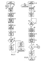
- FIG. 5 and 6 software flow charts illustrate how, and where, these specific needs may be implemented within the normal software necessary for the. proper operation of the LMT.
- an initialization routine is begun at block 132.
- the initialization routine may alternatively be entered as the result of the microprocessor 41 receiving a reset signal as indicated by balloon 133.
- the first step of the initialization routine is represented by block 135 wherein the microprocessor ports and the internal microprocessor timer are initialized.
- the parameters of the signal receiver and conditioner 29 are initialized.
- the message decode parameters and the load control functions, respectively are initialized.
- the diagnostic signal 45 is set in the high state.
- Fig. 6 is a flow chart illustrating the main program loop of the present invention.
- the main program loop is begun at block 161.
- the main program loop may alternatively be entered from the end of the initialization loop as shown by block 159.
- the first step in the main program loop is to decrement a timer reset counter as shown by block 163.
- the diagnostic signal 45 is then set high as shown by block 164.
- decision step 166 a determination is made as to whether an internal clock signal has changed state. If the clock signal has not changed state the microprocessor 41 pauses until the clock signal changes state. When the clock signal has changed state, the microprocessor 41 executes a series of load control commands as shown by block 168.
- the microprocessor 41 executes a series of time keeping commands as shown by block 170.
- the commands included in these blocks are for decrementing individual load timers, producing commands for reconnecting a load to the power distribution network in response to individual load timers, maintaining alternate time bases, and the like.
- step 172 the microprocessor 41 increments the timer reset counter.
- Decision step 174 determines if the timer reset counter is greater than or equal to twenty-six. If the main program loop has been performed 26 or more times without receiving an interrupt signal, the presumption is that the LMT has malfunctioned and should be reset as illustrated by balloon 133. Under normal conditions the timer reset counter will be less than twenty-six and the microprocessor will set the diagnostic signal 45 low as shown by block 176. After the diagnostic signal has been set low the main program loop ends as shown by block 177. At this point, the main program loop may be executed again in which case the microprocessor 41 will return to step 161.
Description
- This invention relates to a load management terminal according to claim 1.
- Several types of distribution network communication systems exist for communicating over the power-line conductors of a utility's power distribution network. The purpose of the communication system is to allow a central control station to communicate with individual or groups of utility customers. Such communications may include instructions for data acquisition or load control. In order to receive and implement these instructions the utility customer location must be equipped with some type of equipment responsive to the received instructions, such as a load management terminal.
- A typical load management terminal is capable of receiving communication signals, determining which of the received signals were addressed to it, and taking appropriate action in response. Appropriate action may be to interrogate a time of day meter, shed specific loads or update a local clock. The load management terminal is also capable of transmitting meter data and other information from the customer location, through the distribution network, back to the electric utility.
- In order to perform all of these functions and still be capable of mass production at cost effective prices, load management terminals are typically designed around a microprocessor. The microprocessor can perform a variety of functions such as comparing the address of a received signal to stored addresses, performing an error check on the received signal, etc.,'while discrete circuits and output devices, under microprocessor control, perform other necessary functions such as receiving or transmitting a communication signal, disconnecting loads, ets. The microprocessor based load management terminal is dependent upon the proper operation of the microprocessor in order to function without problems.
- A microprocessor requires a set of commands, or instructions, in order to perform its intended function, It is possible for a microprocessor to become lost and to begin to execute instructions out of sequence, or to execute phantom instructions, as a result of electrical noise, system transients or the like. When the microprocessor becomes lost it must be reset, or directed to a specific instruction within a program, in order to return to a proper state of operation.
- The chief object of the present invention is to provide a load management terminal control logic circuit to obviate the above-mentioned problems and provide improved operating reliability.
- With this object in view, the invention resides in a load management terminal, control logic curcuit for producing system control signals in a power distribution system, said control logic circuit comprising: memory means containing preprogrammed instructions; a microprocessor producing a diagnostic signal, said diagnostic signal being in a low state in response to one of said instructions and being in a high state in response to another of said instructions, said microprocessor also producing said system control signals; a first timer responsive to said low state of said diagnostic signal, said first timer producing a first reset signal when the time during which said diagnostic signal is in said low state exceeds a predetermined time, said first reset signal input to said microprocessor to effect a reset thereof; and a second timer responsive to said high state of said diagnostic signal, said second timer producing a second reset signal when the time during which said diagnostic signal is in said high state exceeds a predetermined time, said second reset signal input to said microprocessor to effect a reset thereof, said first and second timers comprising the reset circuit.
- The invention will become more readily apparent from the following exemplary description, taken in connection with the accompanying drawings in which:
- Figure 1 is a block diagram illustrating a load management terminal constructed according to the teachings of the present invention;
- Fig. 2 is a block diagram illustrating a microprocessor and a reset circuit constructed according to the teachings of the present invention;
- Fig. 3 is a timing diagram illustrating the diagnostic signal;
- Fig. 4 is an electrical schematic illustrating the circuit details of Fig. 2;
- Fig. 5 is a flow chart illustrating the initialization routing of the present invention; and
- Fig. 6 is a flow chart illustrating the normal operating routing of the present invention.
- The present disclosure reveals a load management terminal having improved reliability and performing an additional load control function. The load management terminal is utilized as an end device in a utility's distribution network communication system. The distribution network carries electrical power as well as communication signals. The load management terminal is comprised of a power-line coupling unit for connecting the load management terminal to the power distribution network. A signal receiver and conditioning unit produces a command signal in response to the power-line coupling unit. A solid state memory contains preprogrammed data and instructions. A microprocessor performs load management functions in response to the command signal. The microprocessor additionally produces a diagnostic signal being in a low state in response to one of the instructions and being in a high state in response to another of the instructions.
- A reset circuit is comprised of a first timer responsive to the low state of the diagnostic signal and a second timer responsive to the high state of the diagnostic signal. The first and second timers cooperate to monitor the microprocessor and to reset the microprocessor whenever it becomes lost.
- Fig. '1 is a block diagram illustrating a load management terminal (hereinafter LMT) 13 constructed according to the teachings of the present invention. Fig. 1 also illustrates in block diagram form the typical environment in which the LMT 13 is found. A primary feeder 15 of a utility's power distribution network is connected to a
conductor 17 through adistribution transformer 19. Theconductor 17 is used to deliver electrical power to a plurality of customer sites, atypical customer site 20 being illustrated in Fig. 1. Electrical power is delivered to a plurality ofloads 21 and 23 within thecustomer site 20. The electrical power is delivered through anelectric energy meter 25 of the type having an encoding register and being capable of producing apulse signal 26 representative of the electric energy consumption. Theloads 21 and 23 together with theelectric energy meter 25 and the LMT 13 make up thecustomer site 20. - The LMT 13 is comprised of a power-
line coupling unit 27 which connects the LMT to the power distribution system. A signal receiver andconditioner 29 is responsive to thecoupling unit 27 to provide command signals in response to received communication signals. The command signals are input to acontrol logic circuit 31. Thecontrol logic circuit 31 is comprised of several components including a microprocessor and a reset circuit which are described in further detail in conjunction with Fig. 2 hereinbelow. - A read only memory 32 contains programmed information and instructions necessary for the proper operation of the LMT 13. A read/write memory 33 contains meter readings, time of day information, scratch pad calculations and the like. The
control logic circuit 31 controls a plurality ofload control switches 35. Thecontrol logic circuit 31 also receives thepulse signal 26. Thecontrol logic circuit 31 provides a plurality of functions such as interrogating theelectric energy meter 25 and opening and closingload control switches 35 thereby removing and adding loads to the power distribution network in response to appropriate command signals. - The LMT 13 additionally includes a
power supply 37 producing regulated supply voltages for the LMT. One of the supply voltages V is monitored bypower fail detector 59. A reset signal produced by thepower fail detector 59 is input to thecontrol logic circuit 31. Thepower fail detector 59 is discussed in further detail in conjunction with Figs. 2 and 4. - Turning to Fig. 2 a block diagram illustrating the
microprocessor 41 and thereset circuit 43 of thecontrol logic circuit 31 is shown. Themicroprocessor 41 produces adiagnostic signal 45 in response to preprogrammed instructions. Thediagnostic signal 45 is input to both alow timer 47 and ahigh timer 49. Thelow timer 47 produces afirst reset signal 50 which is input to aNAND gate 53. Thehigh timer 49 produces asecond reset signal 51 which is also input to theNAND gate 53. An output signal of theNAND gate 53 is input to aNOR gate 55. An output signal of theNOR gate 55 is input to an interrupt request input terminal IRQ of themicroprocessor 41. The output signal of theNOR gate 55 is also input to areset timer 57. An output signal of thereset timer 57 is input to a reset input terminal R of themicroprocessor 41, an inhibit input terminal of thelow timer 47 and an inhibit input terminal of thehigh timer 49. Finally, Fig. 2 illustrates thepower fail detector 59 which produces athird reset signal 60 in response to the regulated supply voltage V. Thethird reset signal 60 is input to the NORgate 55. - The operation of the
reset circuit 43 shown in Fig. 2 may be more easily understood by referring to Fig. 3 wherein a detailed timing diagram of thediagnostic signal 45 is illustrated. During startup, from time To to time Ti, themicroprocessor 41 inhibits both thelow timer 47 and thehigh timer 49 from operating. At time T, themicroprocessor 41 executes an initialization routine wherein one of the early instructions is to set the diagnostic signal in high state. One of the last instructions of the initialization routine instructs the microprocessor to set the diagnostic signal to the low state as shown at time T2. From time T2 to time T3 the diagnostic signal is in the low state. At time T3 the normal operating routine begins and the microprocessor is instructed to set the diagnostic signal in the high state. The diagnostic signal remains in the high state until the end of the normal operating routine when it is again set to the low state as shown at time T4. In this manner, a pattern is developed wherein thediagnostic signal 45 spends a predetermined time in the high state and a predetermined time in the low state. By having a very short time period during which thediagnostic signal 45 is in the low state, and by locating this time period between the end and the beginning of the normal operating routine, a very secure method of determining whether themicroprocessor 41 properly executes this crucial "turnaround", and hence the proper operation of the microprocessor is established. Those skilled in the art will recognize that such a pattern may be established using times other than at the beginning and at the end of the normal operating routine. - The
low time 47 is responsive to the time during which thediagnostic signal 45 is in the low state. As shown in Fig. 3, the time thediagnostic signal 45 is in the low state should not exceed the time period between time T4 and time Ts, for example. If the time during which thediagnostic signal 45 exceeds this predetermined time period the assumption is that themicroprocessor 41 is lost and must be reset. Thelow timer 47 produces thefirst reset signal 50 in response to this condition. - Similarly, the
high timer 49 is responsive to the time during which thediagnostic signal 45 is in the high state. The time during which thediagnostic signal 45 is in the high state should not exceed the time period between time T3 and time T4, for example. If thediagnostic signal 45 remains in the high state beyond this predetermined time period the assumption again is that themicroprocessor 41 is lost and must be reset. Thehigh timer 49 produces the second reset signal in response to this condition. - The first and second reset signals 50 and 51, respectively, propagate through the
gates microprocessor 41 and thereset timer 57. Upon receipt of one of the reset signals at the interrupt request input terminal IRQ themicroprocessor 41 performs an interrupt subroutine for protecting the read/write memory 33. Thereset timer 57 delays the reset signals so as to allow enough time for themicroprocessor 41 to complete the interrupt subroutine before the microprocessor is reset. - The
power failure detector 59 produces thethird reset signal 60 whenever the supply voltage V falls below a predetermined voltage level. Thethird reset signal 60 propagates through thegate 55 to initiate the interrupt subroutine in a similar fashion to the first and second reset signals 50 and 51, respectively. Thethird reset signal 60 is delayed by thereset timer 57 such that the interrupt subroutine is completed. However, thethird reset signal 60 will hold themicroprocessor 41 in the reset condition until the supply voltages return to acceptable levels. - Fig. 4 is an electrical schematic illustrating the circuit details of the components shown in Fig. 2. The
microprocessor 41 produces thediagnostic signal 45 which is input to aninverter 62. An output terminal of theinverter 62 is connected to an inputterminal of a Schmitt trigger 64through adiode 65. The input terminal of theSchmitt trigger 64 is connected to a positive voltage source through aresistor 66, to ground through acapacitor 67 and to the reset terminal R of themicroprocessor 41 through adiode 68. Thefirst reset signal 50 is available at an output terminal of theSchmitt trigger 64. Theinverter 62 and theSchmitt trigger 64 together with the associated components provide the function of thelow timer 47 shown in Fig. 2. - In operation, when the
diagnostic signal 45 is in the high state the signal available at the output terminal of theinverter 62 is in a low state. Thecapacitor 67 is thus normally discharged and the first reset signal is normally in a high state. When thediagnostic signal 45 is in the low state the signal at the output terminal of theinverter 62 is in the high state thus allowing thecapacitor 67 to charge. If thediagnostic signal 45 remains in the low state for an abnormally long time, thecapacitor 67 will charge to a sufficient value such that thefirst reset signal 50 will change from high to a low state. This change in state of thefirst reset signal 50 will only occur should thediagnostic signal 45 remain in the low state for an inappropriate time period. The value of thecapacitor 67 is chosen so as to provide an appropriate limit on the time during which thediagnostic signal 45 is in the low state. - The
diagnostic signal 45 is additionally input to an input terminal of aSchmitt trigger 71 through adiode 72. The input terminal of the aSchmitt trigger 71 is additionally connected to a positive voltage source through aresistor 73, to ground through acapacitor 74 and to the reset input terminal R of themicroprocessor 41 through adiode 75. Thesecond reset signal 51 is available at an output terminal of theinverter 71. TheSchmitt trigger 71 and associated components provide the function of thehigh timer 49 shown in Fig. 2. - In operation, the
capacitor 74 is normally discharged. Thesecond reset signal 51 is normally in a high state in response to thecapacitor 74 being discharged. When thediagnostic signal 45 is in the high state thecapacitor 74 begins to charge. If thediagnostic signal 45 remains in the high state for an inappropriate period of time, thecapacitor 74 will charge to a sufficient voltage level such that theSchmitt trigger 71 will have a high signal input thereto. In response to this condition thesecond reset signal 51 will change from a high to a low state. The value of thecapacitor 74 is chosen so as to provide an appropriate limit on the time during which thediagnostic signal 45 is in the high state. - The
reset timer 57 shown in Fig. 2 is comprised of afirst inverter 78 having an input terminal responsive to the output terminal of the NORgate 55. An output terminal of theinverter 78 is connected to an input terminal of aSchmitt trigger 79 through adiode 80. The input terminal of theSchmitt trigger 79 is connected to a positive voltage source through aresistor 81 and is connected to ground through a capacitor 82. An output terminal of theSchmitt trigger 79 is connected to an input terminal of aSchmitt trigger 84 through adiode 85. The input terminal of theSchmitt trigger 84 is connected to ground through acapacitor 88 and is connected to a positive voltage source through the parallel combination of aresistor 86 and adiode 87. An output terminal of theSchmitt trigger 84 is connected to a base terminal of atransistor 91 through aresistor 92. An emitter terminal of thetransistor 91 is connected to ground. A collector terminal of thetransistor 91 is connected to the reset-input terminal R of themicroprocessor 41 through aconductor 94. The reset input terminal R of themicroprocessor 41 is additionally connected to a positive voltage source through aresistor 98. The interrupt request input terminal IRQ of themicroprocessor 41 is connected to the output terminal of the NORgate 55 through aconductor 95. - Under normal operating conditions, the voltage on the
conductors gate 55 the voltage onconductor 95 is immediately pulled low thereby causing themicroprocessor 41 to perform the interrupt subroutine. The voltage in theconductor 94 is not pulled low until after a predetermined delay, caused by thereset timer 57, so as to allow themicroprocessor 41 to complete the interrupt subroutine before being reset. - The details of the operation of the
reset timer 57 are as follows. The signal available at the output terminal of theinverter 78 is normally in a low state such that the capacitor 82 is normally discharged. The signal available at the output terminal of theSchmitt trigger 79 is normally in a high state such that thecapacitor 88 is charged. The signal available at the output terminal of ths Schmitt trigger 84 is normally in a low state such that thetransistor 91 is nonconductive. When thetransistor 91 is nonconductive the voltage available through theresistor 98 is directly applied to the reset input terminal R of themicroprocessor 41. When a reset signal propagates through the NORgate 55 and theinverter 78, its propagation through the remainder of thereset timer 57 is delayed while the capacitor 82 charges up. Once the capacitor 82 has charged, the reset signal propagates through the remainder of thereset timer 57 causing thetransistor 91 to become conductive. With thetransistor 91 conductive the voltage on theconductor 94 is pulled low thereby causing a reset of themicroprocessor 41. Thus, the value of the capacitor 82 determines the delay effected by thereset timer 57. Additionally, with the voltage on theconductor 94 pulled low both thelow timer 47 and thehigh timer 49 are inhibited since neithercapacitor - Another feature of the reset timer is the charging time of the
capacitor 88. Although thecapacitor 88 provides no delay for the reset signals, it does provide a delay when power is initially turned on. This delay is used to insure that the supply voltages for the LMT are stabilized. - The remaining components to be described in Fig. 4 are those which comprise the
power fail detector 59. An unregulated source voltage V is input to an inverting input terminal of anoperational amplifier 100 through the series combination ofresistor resistors resistor 103. The unregulated source voltage V is additionally connected to ground through the series combination of aresistor 106 and azener diode 107. The junction of theresistor 106 and thezener diode 107 is connected to a non-inverting input terminal of theoperational amplifier 100 through aresistor 108. The non-inverting input terminal of theoperational amplifier 100 is connected to an output terminal thereof through a resistor 111. The output terminal of theoperational amplifier 100 is connected to a positive voltage source through aresistor 112. Thethird reset signal 60 is available at the output terminal of theoperational amplifier 100. Theoperational amplifier 100 acts as a comparator and causes thethird reset signal 60 to change state in response to the supply voltage going out of regulation. - A certain amount of software is necessary in order for the LMT 13 disclosed herein to benefit from the
reset circuit 43. Specifically, themicroprocessor 41 must be instructed to set thediagnostic signal 45 in the appropriate state. In Fig. 5 and 6 software flow charts illustrate how, and where, these specific needs may be implemented within the normal software necessary for the. proper operation of the LMT. - Turning first to Fig. 5, an initialization routine is begun at
block 132. The initialization routine may alternatively be entered as the result of themicroprocessor 41 receiving a reset signal as indicated byballoon 133. The first step of the initialization routine is represented byblock 135 wherein the microprocessor ports and the internal microprocessor timer are initialized. Atblock 137 the parameters of the signal receiver andconditioner 29 are initialized. Atblocks step 143 thediagnostic signal 45 is set in the high state. - At
decision step 145, a determination is made whether load control instructions should be executed. This determination is made based on information produced at the customer location and is not considered to be an important feature of the present invention. If loads are to be shed, internal timers are set and the loads are shed atstep 147. After the loads or shed, or if the loads are not to be shed, themicroprocessor 41 will proceed to block 157 where a frequency is selected and the signal receiver andconditioner 29 is started. Atblock 159 the initialization routine ends. - Fig. 6 is a flow chart illustrating the main program loop of the present invention. The main program loop is begun at
block 161. The main program loop may alternatively be entered from the end of the initialization loop as shown byblock 159. The first step in the main program loop is to decrement a timer reset counter as shown byblock 163. Thediagnostic signal 45 is then set high as shown byblock 164. At decision step 166 a determination is made as to whether an internal clock signal has changed state. If the clock signal has not changed state themicroprocessor 41 pauses until the clock signal changes state. When the clock signal has changed state, themicroprocessor 41 executes a series of load control commands as shown byblock 168. After the load control commands have been executed, themicroprocessor 41 executes a series of time keeping commands as shown byblock 170. The execution of the load control commands and the time keeping commands as represented byblocks - At
step 172 themicroprocessor 41 increments the timer reset counter. Decision step 174 determines if the timer reset counter is greater than or equal to twenty-six. If the main program loop has been performed 26 or more times without receiving an interrupt signal, the presumption is that the LMT has malfunctioned and should be reset as illustrated byballoon 133. Under normal conditions the timer reset counter will be less than twenty-six and the microprocessor will set thediagnostic signal 45 low as shown byblock 176. After the diagnostic signal has been set low the main program loop ends as shown byblock 177. At this point, the main program loop may be executed again in which case themicroprocessor 41 will return to step 161.
Claims (9)
Applications Claiming Priority (2)
| Application Number | Priority Date | Filing Date | Title |
|---|---|---|---|
| US252683 | 1981-04-09 | ||
| US06/252,683 US4429366A (en) | 1981-04-09 | 1981-04-09 | Microprocessor-based load management terminal with reset |
Publications (2)
| Publication Number | Publication Date |
|---|---|
| EP0062871A1 EP0062871A1 (en) | 1982-10-20 |
| EP0062871B1 true EP0062871B1 (en) | 1985-08-07 |
Family
ID=22957068
Family Applications (1)
| Application Number | Title | Priority Date | Filing Date |
|---|---|---|---|
| EP82102879A Expired EP0062871B1 (en) | 1981-04-09 | 1982-04-03 | Load management terminal |
Country Status (10)
| Country | Link |
|---|---|
| US (1) | US4429366A (en) |
| EP (1) | EP0062871B1 (en) |
| JP (1) | JPS57180338A (en) |
| KR (1) | KR880002160B1 (en) |
| AU (1) | AU555426B2 (en) |
| BR (1) | BR8201998A (en) |
| CA (1) | CA1177927A (en) |
| DE (1) | DE3265175D1 (en) |
| FI (1) | FI821239L (en) |
| ZA (1) | ZA822314B (en) |
Cited By (1)
| Publication number | Priority date | Publication date | Assignee | Title |
|---|---|---|---|---|
| CN102723701A (en) * | 2012-06-20 | 2012-10-10 | 湖州电力局 | Remote optical signal locking protection device |
Families Citing this family (27)
| Publication number | Priority date | Publication date | Assignee | Title |
|---|---|---|---|---|
| US4751673A (en) * | 1982-03-22 | 1988-06-14 | The Babcock & Wilcox Company | System for direct comparison and selective transmission of a plurality of discrete incoming data |
| DE3373759D1 (en) * | 1982-06-09 | 1987-10-22 | Fujitsu Ltd | One-chip semiconductor device incorporating a power-supply-potential detecting circuit with reset function |
| DE3322242A1 (en) * | 1982-07-23 | 1984-01-26 | Robert Bosch Gmbh, 7000 Stuttgart | DEVICE FOR FUNCTION MONITORING OF ELECTRONIC DEVICES, IN PARTICULAR MICROPROCESSORS |
| GB2145254A (en) * | 1983-08-17 | 1985-03-20 | Philips Electronic Associated | Domestic electrical appliance |
| US4586179A (en) * | 1983-12-09 | 1986-04-29 | Zenith Electronics Corporation | Microprocessor reset with power level detection and watchdog timer |
| US4627060A (en) * | 1984-11-29 | 1986-12-02 | Baxter Travenol Laboratories, Inc. | Watchdog timer |
| CH666771A5 (en) * | 1985-02-15 | 1988-08-15 | Zellweger Uster Ag | CIRCUIT ARRANGEMENT FOR AN ELECTRONIC RADIO CONTROL RECEIVER. |
| US4656593A (en) * | 1985-05-20 | 1987-04-07 | Westinghouse Electric Corp. | Multi-function load controller for carrier load control subsystem |
| US4881070A (en) | 1985-06-21 | 1989-11-14 | Energy Innovations, Inc. | Meter reading methods and apparatus |
| US4672227A (en) * | 1986-03-17 | 1987-06-09 | Westinghouse Electric Corp. | Automatic transfer switch with delay |
| US4811200A (en) * | 1987-05-12 | 1989-03-07 | Motorola, Inc. | Multiple microprocessor watchdog system |
| BE1001163A3 (en) * | 1987-09-11 | 1989-08-01 | Teco Sa | Power management process of electric power network and system for implementing the method. |
| US4977353A (en) * | 1989-08-31 | 1990-12-11 | Minitronics Pty Limited | Communication system for single point emergency lighting |
| US4999575A (en) * | 1989-09-25 | 1991-03-12 | General Electric Company | Power supply and monitor for controlling an electrical load following a power outage |
| EP0822687B1 (en) * | 1996-07-04 | 2010-02-24 | Siemens Aktiengesellschaft | On-board power supply network |
| DE19642844C1 (en) * | 1996-10-17 | 1997-12-11 | Bosch Gmbh Robert | Reset circuit with microprocessor |
| US6112136A (en) * | 1998-05-12 | 2000-08-29 | Paul; Steven J. | Software management of an intelligent power conditioner with backup system option employing trend analysis for early prediction of ac power line failure |
| US6789187B2 (en) * | 2000-12-15 | 2004-09-07 | Intel Corporation | Processor reset and instruction fetches |
| US7210061B2 (en) * | 2003-04-17 | 2007-04-24 | Hewlett-Packard Development, L.P. | Data redundancy for writes using remote storage system cache memory |
| US8816829B2 (en) * | 2004-06-18 | 2014-08-26 | Wilfried Beck | Household appliance control system |
| EP1794895B8 (en) * | 2004-09-29 | 2019-02-27 | Beck, Wilfried | Data transmission method and device for a/c systems |
| US7595467B2 (en) * | 2005-12-01 | 2009-09-29 | Promos Technologies Inc. | Fault detection system and method for managing the same |
| CN101030080B (en) * | 2006-03-01 | 2010-08-25 | 茂德科技股份有限公司 | Fault inspecting system and its management |
| US20070223165A1 (en) * | 2006-03-22 | 2007-09-27 | Itri Benedict A | Line powering in a multi-line environment |
| AU2007203363B2 (en) | 2006-07-26 | 2010-12-23 | Thomas & Betts International, Inc. | Emergency lighting system |
| CN104460660B (en) * | 2014-12-05 | 2017-08-11 | 国家电网公司 | Remote debugger for remote debugging system |
| EP3416059A1 (en) * | 2017-06-16 | 2018-12-19 | Vestel Elektronik Sanayi ve Ticaret A.S. | Hardware watchdog circuit and method |
Family Cites Families (5)
| Publication number | Priority date | Publication date | Assignee | Title |
|---|---|---|---|---|
| DE2630969B2 (en) * | 1976-07-08 | 1980-06-12 | Heliowatt Werke Elektrizitaets-Gesellschaft Mbh, 1000 Berlin | Electronic maximum counter |
| US4072852A (en) * | 1976-08-23 | 1978-02-07 | Honeywell Inc. | Digital computer monitoring and restart circuit |
| US4096560A (en) * | 1977-10-28 | 1978-06-20 | Rockwell International Corporation | Protection circuit to minimize the effects of power line interruptions on the contents of a volatile electronic memory |
| DE2851190C3 (en) * | 1978-11-27 | 1981-06-11 | Nsm-Apparatebau Gmbh & Co Kg, 6530 Bingen | Fault protection arrangement |
| DE2910058A1 (en) * | 1979-03-14 | 1980-09-18 | Pietzsch Ludwig | Continuous monitoring of crane load limiter computer and memory - using self comparison of memory contents test character and stopping operation when difference arises |
-
1981
- 1981-04-09 US US06/252,683 patent/US4429366A/en not_active Expired - Fee Related
-
1982
- 1982-03-31 CA CA000400012A patent/CA1177927A/en not_active Expired
- 1982-03-31 AU AU82195/82A patent/AU555426B2/en not_active Ceased
- 1982-04-02 ZA ZA822314A patent/ZA822314B/en unknown
- 1982-04-03 EP EP82102879A patent/EP0062871B1/en not_active Expired
- 1982-04-03 DE DE8282102879T patent/DE3265175D1/en not_active Expired
- 1982-04-07 FI FI821239A patent/FI821239L/en not_active Application Discontinuation
- 1982-04-07 BR BR8201998A patent/BR8201998A/en unknown
- 1982-04-08 JP JP57057452A patent/JPS57180338A/en active Pending
- 1982-04-09 KR KR8201567A patent/KR880002160B1/en active
Cited By (1)
| Publication number | Priority date | Publication date | Assignee | Title |
|---|---|---|---|---|
| CN102723701A (en) * | 2012-06-20 | 2012-10-10 | 湖州电力局 | Remote optical signal locking protection device |
Also Published As
| Publication number | Publication date |
|---|---|
| ZA822314B (en) | 1983-05-25 |
| EP0062871A1 (en) | 1982-10-20 |
| KR880002160B1 (en) | 1988-10-17 |
| AU8219582A (en) | 1982-10-14 |
| BR8201998A (en) | 1983-03-15 |
| JPS57180338A (en) | 1982-11-06 |
| US4429366A (en) | 1984-01-31 |
| DE3265175D1 (en) | 1985-09-12 |
| FI821239L (en) | 1982-10-10 |
| KR840000093A (en) | 1984-01-30 |
| AU555426B2 (en) | 1986-09-25 |
| FI821239A0 (en) | 1982-04-07 |
| CA1177927A (en) | 1984-11-13 |
Similar Documents
| Publication | Publication Date | Title |
|---|---|---|
| EP0062871B1 (en) | Load management terminal | |
| US4888495A (en) | Power adapter for electrical installations and especially domestic installations with so-called carrier current control | |
| US4672501A (en) | Circuit breaker and protective relay unit | |
| US7411315B2 (en) | Battery communication system | |
| US5576700A (en) | Apparatus and method for controlling an electrical load and monitoring control operations and the electrical load | |
| US5717937A (en) | Circuit for selecting and designating a master battery pack in a computer system | |
| US4402059A (en) | Load management terminal | |
| EP0385774B1 (en) | Method and apparatus for power failure protection | |
| WO1990001189A1 (en) | Apparatus for defined switching of a microcomputer to standby mode | |
| EP0473271B1 (en) | Data processing apparatus and power supply therefor | |
| CN112463686A (en) | Board card hot-plug device and method | |
| US6038669A (en) | PLC having power failure compensation function and power failure compensation method | |
| US6308233B1 (en) | Circuit allowing insertion/extraction of a board in a system during normal operation | |
| US5349689A (en) | Apparatus for maintaining reset on microprocessor until after electrical chattering from connection of removable memory cartridge has ceased | |
| US5180927A (en) | Reset device for microprocessor, particularly for automotive applications | |
| CA1160753A (en) | Microprocessor watchdog system | |
| US4943961A (en) | Memory retention system for volatile memory devices | |
| JPH0319996B2 (en) | ||
| JP2605995B2 (en) | Microcomputer system | |
| US11789509B2 (en) | Power-on sequence for a power supply system | |
| Shepherd et al. | A new microprocessor relay for overhead line SCADA applications | |
| RU2106736C1 (en) | Automatic generator of signal for initial setting of microprocessor control system of converter | |
| US4433250A (en) | Power supply control apparatus | |
| JPS5897723A (en) | Interface circuit | |
| JP2614926B2 (en) | Power control system |
Legal Events
| Date | Code | Title | Description |
|---|---|---|---|
| PUAI | Public reference made under article 153(3) epc to a published international application that has entered the european phase |
Free format text: ORIGINAL CODE: 0009012 |
|
| AK | Designated contracting states |
Designated state(s): CH DE FR GB IT |
|
| 17P | Request for examination filed |
Effective date: 19830413 |
|
| ITF | It: translation for a ep patent filed |
Owner name: ING. ZINI MARANESI & C. S.R.L. |
|
| GRAA | (expected) grant |
Free format text: ORIGINAL CODE: 0009210 |
|
| AK | Designated contracting states |
Designated state(s): CH DE FR GB IT LI |
|
| REF | Corresponds to: |
Ref document number: 3265175 Country of ref document: DE Date of ref document: 19850912 |
|
| ET | Fr: translation filed | ||
| PG25 | Lapsed in a contracting state [announced via postgrant information from national office to epo] |
Ref country code: LI Effective date: 19860430 Ref country code: CH Effective date: 19860430 |
|
| PLBE | No opposition filed within time limit |
Free format text: ORIGINAL CODE: 0009261 |
|
| STAA | Information on the status of an ep patent application or granted ep patent |
Free format text: STATUS: NO OPPOSITION FILED WITHIN TIME LIMIT |
|
| 26N | No opposition filed | ||
| GBPC | Gb: european patent ceased through non-payment of renewal fee | ||
| PG25 | Lapsed in a contracting state [announced via postgrant information from national office to epo] |
Ref country code: FR Free format text: LAPSE BECAUSE OF NON-PAYMENT OF DUE FEES Effective date: 19861231 |
|
| REG | Reference to a national code |
Ref country code: CH Ref legal event code: PL |
|
| PG25 | Lapsed in a contracting state [announced via postgrant information from national office to epo] |
Ref country code: DE Effective date: 19870101 |
|
| REG | Reference to a national code |
Ref country code: FR Ref legal event code: ST |
|
| PG25 | Lapsed in a contracting state [announced via postgrant information from national office to epo] |
Ref country code: GB Effective date: 19881121 |