EP0062529A2 - Delay compensation in electromagnetic deflection systems - Google Patents
Delay compensation in electromagnetic deflection systems Download PDFInfo
- Publication number
- EP0062529A2 EP0062529A2 EP82301796A EP82301796A EP0062529A2 EP 0062529 A2 EP0062529 A2 EP 0062529A2 EP 82301796 A EP82301796 A EP 82301796A EP 82301796 A EP82301796 A EP 82301796A EP 0062529 A2 EP0062529 A2 EP 0062529A2
- Authority
- EP
- European Patent Office
- Prior art keywords
- signal
- input signal
- deflection circuit
- correction
- beam position
- Prior art date
- Legal status (The legal status is an assumption and is not a legal conclusion. Google has not performed a legal analysis and makes no representation as to the accuracy of the status listed.)
- Withdrawn
Links
Images
Classifications
-
- H—ELECTRICITY
- H04—ELECTRIC COMMUNICATION TECHNIQUE
- H04N—PICTORIAL COMMUNICATION, e.g. TELEVISION
- H04N9/00—Details of colour television systems
- H04N9/12—Picture reproducers
- H04N9/16—Picture reproducers using cathode ray tubes
- H04N9/28—Arrangements for convergence or focusing
-
- H—ELECTRICITY
- H04—ELECTRIC COMMUNICATION TECHNIQUE
- H04N—PICTORIAL COMMUNICATION, e.g. TELEVISION
- H04N3/00—Scanning details of television systems; Combination thereof with generation of supply voltages
- H04N3/10—Scanning details of television systems; Combination thereof with generation of supply voltages by means not exclusively optical-mechanical
- H04N3/16—Scanning details of television systems; Combination thereof with generation of supply voltages by means not exclusively optical-mechanical by deflecting electron beam in cathode-ray tube, e.g. scanning corrections
- H04N3/22—Circuits for controlling dimensions, shape or centering of picture on screen
- H04N3/23—Distortion correction, e.g. for pincushion distortion correction, S-correction
- H04N3/233—Distortion correction, e.g. for pincushion distortion correction, S-correction using active elements
- H04N3/2335—Distortion correction, e.g. for pincushion distortion correction, S-correction using active elements with calculating means
Definitions
- the present invention relates generally to CRT electron beam deflection systems, and more particularly to the compensation of delays inherent in electromagnetic deflection systems.
- Video type display devices operating over a wide range of horizontal scan rates thus require some means of compensating for the effects of deflection system delays on beam position-related correction signals, such as those for beam convergence or top and bottom raster tilt.
- the present invention solves the above-identified problem by advancing the correction signals an amount sufficient to cancel out the deflection system delay(s).
- the required advance may be provided, for example, through the use of a phase lock loop, but a preferable approach is to add a d.c. level shift to a beam position-related signal from which the correction signal is derived.
- a correction waveform generator for an electromagnetically-deflected video display is compensated for deflection system delays by adding an appropriate d.c. level shift to a ramp signal from which the correction waveforms are derived.
- This d.c. offset causes the correction signals to be time advanced an amount sufficient to compensate for delays in the deflection system and its drive circuitry.
- This delay compensation method i.e., adding a d.c. level shift to a beam position-related ramp signal from which the correction signal is derived -- may be used for both the beam convergence and the vertical raster top and bottom tilt correction signals.
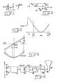
- FIG. 1 illustrates a simplified model of an electromagnetic deflection circuit that includes a CRT deflection coil L, a loss element R representing the effective parallel resistance associated with the coil, and a suitable current source S. It can be shown that for an input current I (t), where the current I L (t) in inductor L is The gain coefficients K' 2 , K' 3 , K' 4 , etc. are small with respect to the coefficients of the corresponding powers of t in I c (t-L/R) when L/R « t A /2, t A being the active time of the CRT's horizontal sweep.
- FIG. 2 illustrates graphically the current I (t) generated by source S.
- the desired correction waveform here a parabola
- the transient resulting from the expoential term K e e -R/Lt will be substantially decayed.
- the field-producing current through the coil thus may be approximated by I L (t) ⁇ I C (t-L/R). Accordingly, the delay produced by loss element R can be compensated by a time advance term +L/R.
- the coil driver circuit shown (in simplified form) in FIG. 3 can be adjusted to cancel the delay produced by the deflection coil's loss element R.
- the circuit includes an operational amplifier OA whose noninverting input is referenced to ground by a resistor R O .
- An input resistor R 1 connected to the amplifier's inverting (-) input is bridged by a capacitor C, and the output of the amplifier is coupled to its inverting input by. a feedback resistor R 2 . If the value of capacitor C is equal to L/R 1 .R, the delay caused by loss element R will be cancelled out.
- the FIG. 3 circuit which acts as a differentiator, has certain drawbacks, however. It is less stable than desired, and does not compensate for other delays in the deflection system.
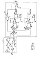
- FIG. 4 A block diagram of a CRT beam deflection system illustrating the preferred practice of the invention is shown in FIG. 4.
- Such a system may be used, for example, to achieve dynamic convergence correction of the beams in a delta-gun color CRT.
- the FIG. 4 deflection system uses beam position information to generate suitable correction waveforms, which are applied to a deflection coil mounted on the CRT.
- the correction function may be expressed as C(X,Y), where C(0,0) is the center of the display screen.
- the terms X and Y represent positions on the horizontal and vertical axes, respectively, of the CRT screen, each term varying in value between -1 and +1.
- the FIG. 4 system includes a pair of adders 10 and 12 for summing beam-shifting signals Xs and Ys with horizontal and vertical beam position signals X and Y, respectively.
- the summed beam position and time shift signals are applied to the appropriate inputs of a correction waveform generator 14, which produces a desired correction signal C(X,Y) at its output.
- Generator 14 may, for example, be a convergence waveform generator of known design, such as the one shown in U.S. Patent 3,942,067 to Cawood.
- the output signal C(X,Y) from correction generator 14 is supplied to a coil driver circuit 16, which provides an output current signal I c (t) to drive a beam deflector 18.
- Deflector 18 includes a deflection coil L and its associated effective parallel resistance R.
- Driver circuit 16 is conventional and may, for example, take the form of a class B linear transconductance amplifier.
- the current through coil L produces a magnetic field B that is coupled into CRT 22 to provide a deflecting field B d in the path of a beam within the tube.
- Color CRTs typically include internal pole pieces near each electron gun for applying convergence correction fields to the beams.
- the delay t D produced by the internal coupling structure is represented in FIG. 4 by a delay block 20.
- the beam shifting signals Xs and Ys are related to time by the expressions where ts is the time advance required to compensate for system delays.
- the correction signal C(X,Y) may be advanced in time to cancel out deflection system delays by suitably shifting the beam position-related signal(s) from which the correction waveform is derived.
- This is accomplished, according to the invention, by applying a d.c. offset to horizontal (or vertical) ramp signals used to generate the correction signals.
- a d.c. offset Xs to a horizontal ramp signal X effectively advances the ramp (i.e., shifts it toward the left side of the screen) an amount ⁇ X corresponding to a time shift ot.
- the effect on a resultant parabolic correction signal C(X,Y) from generator 14 (FIG.
- FIG. 6 illustrates suitable circuitry for the adder 10 and correction generator 14 of FIG. 4 as used in a convergence correction system for a color CRT display.
- Adder 10 includes an operational amplifier 26 receiving at its inverting input a horizontal beam position signal (X) via input terminal 24 and input resistor 28. The non-inverting input of amplifier 26 is referenced to ground potential by resistor 27.
- a feedback resistor 30 paralleled by a capacitor 36 is connected between the output and inverting input of the amplifier.
- a d.c. position shift signal (X ) generated by a potentiometer 32 is applied to the inverting input of amplifier 26 via series resistors 33, 34, whose common junction may be connected to ground via a switch 35.
- the output signal from operational amplifier 26 is of the form (X + X S ).
- the combined signal is indicated simply by X in FIG. 6.
- the position control signal (X ) is controllable by potentiometer 32 to any value required to cancel out delays in the system, or may be disabled by closing switch 35.
- Correction generator 14 includes three multipliers 38, 40, and 42, five differential operational amplifiers 44, 46, 48, 50 and 52, two inverters 54, 56, a variable gain amplifier (or attenuator) 58, two potentiometers 60 and 62, and associated passive elements, which are configured to provide a parabola signal KIX2, and two higher degree correction signals K 2 (X 2 - X 4 ) and K 3 (X - X 3 ). These are, in turn, supplied to the input of summing amplifier 52 to provide the required convergence correction signal from output terminal 64.
- the functions (X - X 4 ) and ( X - X 3 ) are used to provide more precise correction without causing interaction with the parabola signal K 1 X 2 at the right and left sides of the screen.
Landscapes
- Engineering & Computer Science (AREA)
- Multimedia (AREA)
- Signal Processing (AREA)
- Video Image Reproduction Devices For Color Tv Systems (AREA)
- Details Of Television Scanning (AREA)
Abstract
An electromagnetic deflection circuit is disclosed. The deflection circuit includes a plurality of loss elements. These loss elements are responsible for the production of an inherent time delay (<sup>t</sup>D) between the energization of the circuit by an input signal (x, y) and the generation of a magnetic flux (<sup>B</sup>d) used to deflect an electron beam within a cathode-ray tube (22). According to an exemplified embodiment of the invention, a DC level shift signal generator (32, Fig. 6), a beam position input signal generator (24, Fig. 6), and an adder (10) for adding the DC level shift signal to the beam position input signal produce an input signal that energizes the correction deflection circuit (14). The introduction of the DC level to the beam position input signal effectively advances, in time, the output signal from the convergence correction signal generator. This advance compensates for the various time delays present in the deflection circuit.
Description
- The present invention relates generally to CRT electron beam deflection systems, and more particularly to the compensation of delays inherent in electromagnetic deflection systems.
- Television and other CRT-type image display systems typically use a large magnetic yoke to scan the CRT's electron beam(s) over the surface of its phosphor display screen in a raster pattern. Most multicolor cathode-ray tubes have three closely-spaced beams, which must be substantially coincident, or converged, at the screen and remain so as they are deflected over its surface. Thus, in addition to deflection by the common magnetic yoke to produce a scanned raster, each beam is also deflected individually as needed to maintain convergence over the entire screen. This small angle, variable beam deflection, referred to as dynamic convergence, is accomplished by applying correction signals to convergence coils on the neck of the CRT.
- There is an inherent delay (not a pure delay, but instead a complex error function the major part of which is a time shift) between the input current waveform driving a deflection coil and the flux it produces. In a television-type display, the corrections required for beam convergence and for pincushion and tilt distortion of the vertical raster can be significantly affected by such delays. Most such displays operate at fixed, relatively low scan rates -approx. 15 KHz for U.S. commercial television -- at which delays can be tolerated, or compensated using standard controls. However, electromagnetically- deflected CRT displays operating at higher horizontal scan rates encounter a much more severe problem, particularly those designed to operate over a wide range of frequencies. For. example, a delay of six percent of the horizontal width at 60 ps active time (approx. 15 KHz) would increase to 25% of the horizontal width at 14ps active time (approx. 50 KHz). Video type display devices operating over a wide range of horizontal scan rates thus require some means of compensating for the effects of deflection system delays on beam position-related correction signals, such as those for beam convergence or top and bottom raster tilt.
- The present invention solves the above-identified problem by advancing the correction signals an amount sufficient to cancel out the deflection system delay(s). The required advance may be provided, for example, through the use of a phase lock loop, but a preferable approach is to add a d.c. level shift to a beam position-related signal from which the correction signal is derived.
- According to a preferred embodiment of the invention, which is described in greater detail below, a correction waveform generator for an electromagnetically-deflected video display is compensated for deflection system delays by adding an appropriate d.c. level shift to a ramp signal from which the correction waveforms are derived. This d.c. offset causes the correction signals to be time advanced an amount sufficient to compensate for delays in the deflection system and its drive circuitry. This delay compensation method -- i.e., adding a d.c. level shift to a beam position-related ramp signal from which the correction signal is derived -- may be used for both the beam convergence and the vertical raster top and bottom tilt correction signals.
- Further applications of the present invention will become apparent as the following detailed description is read in conjunction with the accompanying drawing.
-
- Fig. 1 is a simplified circuit diagram used in explaining the principle of the present invention;
- Fig. 2 is a time plot of input current Ic(t) in the Fig. 1 circuit;
- Fig. 3 shows a simplified coil driver circuit;
- Fig. 4 is a block diagram of a beam deflection correction system incorporating the present invention;
- Fig. 5 depicts certain waveforms illustrating the delay compensation provided by the Fig. 4 system; and
- Fig. 6 is a schematic diagram of certain circuitry for adapting the Fig. 4 system to correction of beam convergeance.
- Referring now to the drawings, FIG. 1 illustrates a simplified model of an electromagnetic deflection circuit that includes a CRT deflection coil L, a loss element R representing the effective parallel resistance associated with the coil, and a suitable current source S. It can be shown that for an input current I (t), where


- FIG. 2 illustrates graphically the current I (t) generated by source S. By beginning generation of the desired correction waveform (here a parabola) by suitable time -tl prior to the start of the electron beam's active sweep period, which begins at time t=o at the left side of the display screen (X = -1), the transient resulting from the expoential term Kee-R/Lt will be substantially decayed. The field-producing current through the coil thus may be approximated by IL(t) ≈ IC (t-L/R). Accordingly, the delay produced by loss element R can be compensated by a time advance term +L/R.
- The coil driver circuit shown (in simplified form) in FIG. 3 can be adjusted to cancel the delay produced by the deflection coil's loss element R. The circuit includes an operational amplifier OA whose noninverting input is referenced to ground by a resistor RO. An input resistor R1 connected to the amplifier's inverting (-) input is bridged by a capacitor C, and the output of the amplifier is coupled to its inverting input by. a feedback resistor R2. If the value of capacitor C is equal to L/R1.R, the delay caused by loss element R will be cancelled out. The FIG. 3 circuit, which acts as a differentiator, has certain drawbacks, however. It is less stable than desired, and does not compensate for other delays in the deflection system.
- A block diagram of a CRT beam deflection system illustrating the preferred practice of the invention is shown in FIG. 4. Such a system may be used, for example, to achieve dynamic convergence correction of the beams in a delta-gun color CRT. The FIG. 4 deflection system uses beam position information to generate suitable correction waveforms, which are applied to a deflection coil mounted on the CRT. The correction function may be expressed as C(X,Y), where C(0,0) is the center of the display screen. The terms X and Y represent positions on the horizontal and vertical axes, respectively, of the CRT screen, each term varying in value between -1 and +1.
- The FIG. 4 system includes a pair of
adders correction waveform generator 14, which produces a desired correction signal C(X,Y) at its output.Generator 14 may, for example, be a convergence waveform generator of known design, such as the one shown in U.S. Patent 3,942,067 to Cawood. - The output signal C(X,Y) from
correction generator 14 is supplied to acoil driver circuit 16, which provides an output current signal Ic(t) to drive abeam deflector 18.Deflector 18 includes a deflection coil L and its associated effective parallel resistanceR. Driver circuit 16 is conventional and may, for example, take the form of a class B linear transconductance amplifier. The current through coil L produces a magnetic field B that is coupled intoCRT 22 to provide a deflecting field Bd in the path of a beam within the tube. Color CRTs typically include internal pole pieces near each electron gun for applying convergence correction fields to the beams. The delay tD produced by the internal coupling structure is represented in FIG. 4 by adelay block 20. - The beam position-related signals X and Y are related to time by the expressions


- As will be understood from FIG. 4,


- As will by now be evident, the correction signal C(X,Y) may be advanced in time to cancel out deflection system delays by suitably shifting the beam position-related signal(s) from which the correction waveform is derived. This is accomplished, according to the invention, by applying a d.c. offset to horizontal (or vertical) ramp signals used to generate the correction signals. Referring to FIG. 5, it will be seen that the addition of a d.c. offset Xs to a horizontal ramp signal X effectively advances the ramp (i.e., shifts it toward the left side of the screen) an amount ΔX corresponding to a time shift ot. The effect on a resultant parabolic correction signal C(X,Y) from generator 14 (FIG. 4) is shown in the lower portion of the figure. Thus, by applying an appropriate offset to the input ramp, delays inherent in the deflection coil and its associated magnetic structure, as well as those associated with the coil drive circuitry, may be readily compensated. The amount of offset, or time shift, required will be different at different scan rates, and may be varied either mannually or automatically. Moreover, an offset ramp signal used to correct for delays in one deflection system may be used to correct for delays in a different system associated with the same CRT.
- FIG. 6 illustrates suitable circuitry for the
adder 10 andcorrection generator 14 of FIG. 4 as used in a convergence correction system for a color CRT display.Adder 10 includes anoperational amplifier 26 receiving at its inverting input a horizontal beam position signal (X) viainput terminal 24 andinput resistor 28. The non-inverting input ofamplifier 26 is referenced to ground potential by resistor 27. Afeedback resistor 30 paralleled by a capacitor 36 is connected between the output and inverting input of the amplifier. A d.c. position shift signal (X ) generated by apotentiometer 32 is applied to the inverting input ofamplifier 26 viaseries resistors switch 35. - It will be understood that the output signal from
operational amplifier 26 is of the form (X + XS). For convenience, however, the combined signal is indicated simply by X in FIG. 6. The position control signal (X ) is controllable bypotentiometer 32 to any value required to cancel out delays in the system, or may be disabled by closingswitch 35. -
Correction generator 14 includes threemultipliers operational amplifiers inverters potentiometers amplifier 52 to provide the required convergence correction signal from output terminal 64. - The functions (X - X4) and (X - X3) are used to provide more precise correction without causing interaction with the parabola signal K1X2 at the right and left sides of the screen.
- It will be apparent to those skilled in the art that many changes and modifications may be made in the specific circuits and examples given herein. Such variations are not to be regarded as a departure from the scope of the invention, which is limited only as required by the terms of the appended claims and the supporting disclosure.
Claims (6)
1. An electron beam deflection circuit for a cathode ray tube, the circuit including a deflection coil and a signal generator coupled to the coil, the generator providing an' output signal derived from a beam position-related input signal, characterized by the addition to the input signal of a further signal to effect a time advance of the output signal sufficient to substantially cancel time delays inherent in the deflection circuit.
2. The circuit of claim 1, wherein said beam position-related signal is a ramp signal, and said further signal is a d.c. potential.
3. An electromagnetic deflection circuit for deflecting an electron beam being generated in the neck of a cathode ray tube, said deflection circuit having inherent time delays inclusive therein due to a plurality of loss elements in said deflection circuit, comprising:
means for developing an input signal, said input signal energizing said electromagnetic deflection circuit, the means for developing an input signal including,
means for generating a beam position input signal, means for generating a shift signal representative of a DC level increment; and
adder means responsive to said beam position input signal and to said shift signal for adding said shift signal to said beam position input signal thereby introducing said DC level increment into said beam position input signal and producing said input signal in response thereto; and
means responsive to said input signal for developing a magnetic field, said magnetic field deflecting said electron beam being generated in the neck of said cathode ray tube;
whereby the introduction of said DC level increment into said beam position input signal compensates for the inherent time delays produced by the plurality of loss elements in said deflection circuit.
4. An electromagnetic deflection circuit in accordance with claim 3 wherein three electron beams are generated in the neck of said CRT tube; and wherein the means for developing a magnetic field comprises:
correction signal generating means responsive to said input signal for generating a correction signal representative of the amount of correction needed to converge said three electron beams, said correction signal being advanced along the time axis in response to said shift signal representative of said DC level increment.
5. An electromagnetic deflection circuit in accordance with claim 4 wherein the means for developing further comprises;
means responsive to said correction signal for amplifying said signal; and
deflection means responsive to the amplified correction signal for generating a magnetic field, said magnetic field deflecting at least one of the electron beams being generated in the neck of said cathode ray tube.
6. An electromagnetic deflection circuit in accordance with claim 5 wherein the means for amplifying comprises an operational amplifier, one input terminal being connected to a ground potential, another input terminal. being responsive to said correction signal, said another input terminal being connected to a resistor-capacitor parallel combination, the output terminal of said operational amplifier and said another input terminal being connected together via a feedback resistor.
Applications Claiming Priority (2)
| Application Number | Priority Date | Filing Date | Title |
|---|---|---|---|
| JP56049522A JPS57166776A (en) | 1981-04-03 | 1981-04-03 | Electromagnetic deflecting circuit |
| JP49522/81 | 1981-04-03 |
Publications (2)
| Publication Number | Publication Date |
|---|---|
| EP0062529A2 true EP0062529A2 (en) | 1982-10-13 |
| EP0062529A3 EP0062529A3 (en) | 1984-03-21 |
Family
ID=12833463
Family Applications (1)
| Application Number | Title | Priority Date | Filing Date |
|---|---|---|---|
| EP82301796A Withdrawn EP0062529A3 (en) | 1981-04-03 | 1982-04-05 | Delay compensation in electromagnetic deflection systems |
Country Status (3)
| Country | Link |
|---|---|
| US (1) | US4623825A (en) |
| EP (1) | EP0062529A3 (en) |
| JP (1) | JPS57166776A (en) |
Cited By (4)
| Publication number | Priority date | Publication date | Assignee | Title |
|---|---|---|---|---|
| DE3510663A1 (en) * | 1984-03-24 | 1985-10-03 | Victor Company Of Japan, Ltd., Yokohama, Kanagawa | TELEVISION RECEIVER |
| WO1990005428A1 (en) * | 1988-11-08 | 1990-05-17 | Honeywell Inc. | Memory mapped deflection correction system |
| EP0453934A3 (en) * | 1990-04-25 | 1992-03-18 | Deutsche Thomson-Brandt Gmbh | Raster correction device in a television set |
| EP0674433A1 (en) * | 1994-03-24 | 1995-09-27 | Thomson Consumer Electronics, Inc. | Parabolic signal timing loop |
Families Citing this family (5)
| Publication number | Priority date | Publication date | Assignee | Title |
|---|---|---|---|---|
| JPH0771195B2 (en) * | 1987-05-18 | 1995-07-31 | 株式会社日立製作所 | Deflection distortion correction circuit |
| US5138238A (en) * | 1991-05-17 | 1992-08-11 | Thomson Consumer Electronics, Inc. | Arrangement for correcting beam landing location error in a video display |
| US5528112A (en) * | 1994-12-08 | 1996-06-18 | Thomson Consumer Electronics, Inc. | Deflection correction signal generator |
| KR0143254B1 (en) * | 1995-04-28 | 1998-07-15 | 배순훈 | A distortion controlling circuit of a monitor |
| CN102428500B (en) * | 2009-05-18 | 2014-10-29 | 皇家飞利浦电子股份有限公司 | Interpolation free fan-to-parallel beam re-binning |
Family Cites Families (5)
| Publication number | Priority date | Publication date | Assignee | Title |
|---|---|---|---|---|
| US3501669A (en) | 1968-11-29 | 1970-03-17 | Bunker Ramo | Deflection signal correction system |
| US3772566A (en) | 1971-05-07 | 1973-11-13 | Loral Corp | Linearization of magnetically deflected cathode ray tube with non-axial guns |
| US4162434A (en) | 1977-11-07 | 1979-07-24 | Rca Corporation | Regulator with short circuit protection |
| GB2066028A (en) | 1979-12-15 | 1981-07-01 | Ibm | Digitally stored quantities for correction of crt aberrrations |
| US4427926A (en) | 1981-05-18 | 1984-01-24 | Rockwell International Corporation | Dynamic convergence of random scan multi-beam cathode ray tubes |
-
1981
- 1981-04-03 JP JP56049522A patent/JPS57166776A/en active Granted
-
1982
- 1982-04-05 US US06/365,658 patent/US4623825A/en not_active Expired - Fee Related
- 1982-04-05 EP EP82301796A patent/EP0062529A3/en not_active Withdrawn
Cited By (7)
| Publication number | Priority date | Publication date | Assignee | Title |
|---|---|---|---|---|
| DE3510663A1 (en) * | 1984-03-24 | 1985-10-03 | Victor Company Of Japan, Ltd., Yokohama, Kanagawa | TELEVISION RECEIVER |
| US4670790A (en) * | 1984-03-24 | 1987-06-02 | Victor Company Of Japan, Ltd. | Television receiver provided with delay circuit |
| WO1990005428A1 (en) * | 1988-11-08 | 1990-05-17 | Honeywell Inc. | Memory mapped deflection correction system |
| EP0453934A3 (en) * | 1990-04-25 | 1992-03-18 | Deutsche Thomson-Brandt Gmbh | Raster correction device in a television set |
| EP0674433A1 (en) * | 1994-03-24 | 1995-09-27 | Thomson Consumer Electronics, Inc. | Parabolic signal timing loop |
| EP0674431A1 (en) * | 1994-03-24 | 1995-09-27 | Thomson Consumer Electronics, Inc. | Shaped parabolic signal for deflection correction |
| EP0675641A1 (en) * | 1994-03-24 | 1995-10-04 | Thomson Consumer Electronics, Inc. | Parabolic correction signal amplitude control loop |
Also Published As
| Publication number | Publication date |
|---|---|
| EP0062529A3 (en) | 1984-03-21 |
| US4623825A (en) | 1986-11-18 |
| JPS57166776A (en) | 1982-10-14 |
| JPS6257146B2 (en) | 1987-11-30 |
Similar Documents
| Publication | Publication Date | Title |
|---|---|---|
| US3980819A (en) | Edge enhancement for television images | |
| US4623825A (en) | Delay compensation in electromagnetic deflection systems | |
| EP0456942B1 (en) | Deflection yoke arrangement with overlapping deflection coils | |
| US4500816A (en) | Convergence control apparatus for color cathode ray tube display systems | |
| US4249112A (en) | Dynamic focus and astigmatism correction circuit | |
| US5448140A (en) | Image display apparatus with a deflection circuit having function for correcting rotational distortion | |
| US4766354A (en) | Independent top/bottom pincushion correction | |
| EP0173875B1 (en) | Dynamic focus signal shaper | |
| US4707639A (en) | Dynamic focus voltage with phase compensated adjustment | |
| US2869026A (en) | Cathode ray sweep correction system | |
| US4496882A (en) | Inductorless pincushion correction circuit | |
| GB2085698A (en) | Stigmator for cathode ray tube | |
| US5367212A (en) | Geometry correction waveform synthesizer | |
| CA1225750A (en) | Convergence control system for multigun crt | |
| US4524307A (en) | Convergence control system for multigun CRT | |
| US4501996A (en) | Deflection distortion correcting circuit | |
| US4410840A (en) | Color cathode ray tube display apparatus with compensation for errors due to interfering magnetic fields | |
| US5936363A (en) | User controlled deflection apparatus for correcting upper and lower distortions of a CRT | |
| EP0660364B1 (en) | Display device comprising a deflection unit | |
| US4223252A (en) | Color switching display system | |
| US4639644A (en) | High voltage dynamic focusing system | |
| EP0642262B1 (en) | Automatic calibration in a waveform generator for deflection | |
| JPH0134454Y2 (en) | ||
| JP2907868B2 (en) | Horizontal deflection distortion automatic correction display | |
| US5091681A (en) | CRT dynamic focus system having independent corner adjustment |
Legal Events
| Date | Code | Title | Description |
|---|---|---|---|
| PUAI | Public reference made under article 153(3) epc to a published international application that has entered the european phase |
Free format text: ORIGINAL CODE: 0009012 |
|
| AK | Designated contracting states |
Designated state(s): BE DE GB NL |
|
| PUAL | Search report despatched |
Free format text: ORIGINAL CODE: 0009013 |
|
| AK | Designated contracting states |
Designated state(s): BE DE GB NL |
|
| 17P | Request for examination filed |
Effective date: 19840914 |
|
| STAA | Information on the status of an ep patent application or granted ep patent |
Free format text: STATUS: THE APPLICATION IS DEEMED TO BE WITHDRAWN |
|
| 18D | Application deemed to be withdrawn |
Effective date: 19851010 |
|
| RIN1 | Information on inventor provided before grant (corrected) |
Inventor name: WAHLQUIST, CLAYTON CHARLES Inventor name: OLMSTEAD, HAROLD WAYNE |