EP0057586A2 - Raster output scanner and method - Google Patents
Raster output scanner and method Download PDFInfo
- Publication number
- EP0057586A2 EP0057586A2 EP82300463A EP82300463A EP0057586A2 EP 0057586 A2 EP0057586 A2 EP 0057586A2 EP 82300463 A EP82300463 A EP 82300463A EP 82300463 A EP82300463 A EP 82300463A EP 0057586 A2 EP0057586 A2 EP 0057586A2
- Authority
- EP
- European Patent Office
- Prior art keywords
- velocity
- imaging member
- clock
- frequency
- signal
- Prior art date
- Legal status (The legal status is an assumption and is not a legal conclusion. Google has not performed a legal analysis and makes no representation as to the accuracy of the status listed.)
- Granted
Links
- 238000000034 method Methods 0.000 title claims abstract description 11
- 238000003384 imaging method Methods 0.000 claims abstract description 48
- 230000001360 synchronised effect Effects 0.000 claims description 4
- 239000003990 capacitor Substances 0.000 description 7
- 230000000903 blocking effect Effects 0.000 description 4
- 230000003287 optical effect Effects 0.000 description 4
- 230000007423 decrease Effects 0.000 description 3
- 230000001419 dependent effect Effects 0.000 description 3
- 230000000694 effects Effects 0.000 description 3
- 238000012360 testing method Methods 0.000 description 3
- 230000004308 accommodation Effects 0.000 description 2
- 239000013078 crystal Substances 0.000 description 2
- 238000012544 monitoring process Methods 0.000 description 2
- 238000012546 transfer Methods 0.000 description 2
- 238000004804 winding Methods 0.000 description 2
- 230000001133 acceleration Effects 0.000 description 1
- 238000004140 cleaning Methods 0.000 description 1
- 238000012937 correction Methods 0.000 description 1
- 230000003247 decreasing effect Effects 0.000 description 1
- 230000001934 delay Effects 0.000 description 1
- 230000003111 delayed effect Effects 0.000 description 1
- 238000011161 development Methods 0.000 description 1
- 238000005286 illumination Methods 0.000 description 1
- 239000000463 material Substances 0.000 description 1
- 238000005259 measurement Methods 0.000 description 1
- 238000012986 modification Methods 0.000 description 1
- 230000004048 modification Effects 0.000 description 1
- 229910000402 monopotassium phosphate Inorganic materials 0.000 description 1
- 235000019796 monopotassium phosphate Nutrition 0.000 description 1
- 230000000737 periodic effect Effects 0.000 description 1
- PJNZPQUBCPKICU-UHFFFAOYSA-N phosphoric acid;potassium Chemical compound [K].OP(O)(O)=O PJNZPQUBCPKICU-UHFFFAOYSA-N 0.000 description 1
- 238000012545 processing Methods 0.000 description 1
- 230000005855 radiation Effects 0.000 description 1
- 239000007787 solid Substances 0.000 description 1
- 239000000758 substrate Substances 0.000 description 1
- 238000012549 training Methods 0.000 description 1
- 238000011144 upstream manufacturing Methods 0.000 description 1
Images
Classifications
-
- H—ELECTRICITY
- H04—ELECTRIC COMMUNICATION TECHNIQUE
- H04N—PICTORIAL COMMUNICATION, e.g. TELEVISION
- H04N1/00—Scanning, transmission or reproduction of documents or the like, e.g. facsimile transmission; Details thereof
- H04N1/04—Scanning arrangements, i.e. arrangements for the displacement of active reading or reproducing elements relative to the original or reproducing medium, or vice versa
- H04N1/047—Detection, control or error compensation of scanning velocity or position
-
- H—ELECTRICITY
- H04—ELECTRIC COMMUNICATION TECHNIQUE
- H04N—PICTORIAL COMMUNICATION, e.g. TELEVISION
- H04N1/00—Scanning, transmission or reproduction of documents or the like, e.g. facsimile transmission; Details thereof
- H04N1/04—Scanning arrangements, i.e. arrangements for the displacement of active reading or reproducing elements relative to the original or reproducing medium, or vice versa
- H04N1/113—Scanning arrangements, i.e. arrangements for the displacement of active reading or reproducing elements relative to the original or reproducing medium, or vice versa using oscillating or rotating mirrors
- H04N1/1135—Scanning arrangements, i.e. arrangements for the displacement of active reading or reproducing elements relative to the original or reproducing medium, or vice versa using oscillating or rotating mirrors for the main-scan only
-
- H—ELECTRICITY
- H04—ELECTRIC COMMUNICATION TECHNIQUE
- H04N—PICTORIAL COMMUNICATION, e.g. TELEVISION
- H04N1/00—Scanning, transmission or reproduction of documents or the like, e.g. facsimile transmission; Details thereof
- H04N1/04—Scanning arrangements, i.e. arrangements for the displacement of active reading or reproducing elements relative to the original or reproducing medium, or vice versa
- H04N1/12—Scanning arrangements, i.e. arrangements for the displacement of active reading or reproducing elements relative to the original or reproducing medium, or vice versa using the sheet-feed movement or the medium-advance or the drum-rotation movement as the slow scanning component, e.g. arrangements for the main-scanning
-
- H—ELECTRICITY
- H04—ELECTRIC COMMUNICATION TECHNIQUE
- H04N—PICTORIAL COMMUNICATION, e.g. TELEVISION
- H04N2201/00—Indexing scheme relating to scanning, transmission or reproduction of documents or the like, and to details thereof
- H04N2201/024—Indexing scheme relating to scanning, transmission or reproduction of documents or the like, and to details thereof deleted
- H04N2201/02406—Arrangements for positioning elements within a head
- H04N2201/02416—Rotational positioning, i.e. with respect to an axis
-
- H—ELECTRICITY
- H04—ELECTRIC COMMUNICATION TECHNIQUE
- H04N—PICTORIAL COMMUNICATION, e.g. TELEVISION
- H04N2201/00—Indexing scheme relating to scanning, transmission or reproduction of documents or the like, and to details thereof
- H04N2201/024—Indexing scheme relating to scanning, transmission or reproduction of documents or the like, and to details thereof deleted
- H04N2201/02406—Arrangements for positioning elements within a head
- H04N2201/02439—Positioning method
-
- H—ELECTRICITY
- H04—ELECTRIC COMMUNICATION TECHNIQUE
- H04N—PICTORIAL COMMUNICATION, e.g. TELEVISION
- H04N2201/00—Indexing scheme relating to scanning, transmission or reproduction of documents or the like, and to details thereof
- H04N2201/04—Scanning arrangements
- H04N2201/047—Detection, control or error compensation of scanning velocity or position
- H04N2201/04701—Detection of scanning velocity or position
- H04N2201/0471—Detection of scanning velocity or position using dedicated detectors
-
- H—ELECTRICITY
- H04—ELECTRIC COMMUNICATION TECHNIQUE
- H04N—PICTORIAL COMMUNICATION, e.g. TELEVISION
- H04N2201/00—Indexing scheme relating to scanning, transmission or reproduction of documents or the like, and to details thereof
- H04N2201/04—Scanning arrangements
- H04N2201/047—Detection, control or error compensation of scanning velocity or position
- H04N2201/04701—Detection of scanning velocity or position
- H04N2201/04715—Detection of scanning velocity or position by detecting marks or the like, e.g. slits
- H04N2201/04722—Detection of scanning velocity or position by detecting marks or the like, e.g. slits on a photoconductive drum or belt
-
- H—ELECTRICITY
- H04—ELECTRIC COMMUNICATION TECHNIQUE
- H04N—PICTORIAL COMMUNICATION, e.g. TELEVISION
- H04N2201/00—Indexing scheme relating to scanning, transmission or reproduction of documents or the like, and to details thereof
- H04N2201/04—Scanning arrangements
- H04N2201/047—Detection, control or error compensation of scanning velocity or position
- H04N2201/04701—Detection of scanning velocity or position
- H04N2201/04729—Detection of scanning velocity or position in the main-scan direction
-
- H—ELECTRICITY
- H04—ELECTRIC COMMUNICATION TECHNIQUE
- H04N—PICTORIAL COMMUNICATION, e.g. TELEVISION
- H04N2201/00—Indexing scheme relating to scanning, transmission or reproduction of documents or the like, and to details thereof
- H04N2201/04—Scanning arrangements
- H04N2201/047—Detection, control or error compensation of scanning velocity or position
- H04N2201/04701—Detection of scanning velocity or position
- H04N2201/04731—Detection of scanning velocity or position in the sub-scan direction
-
- H—ELECTRICITY
- H04—ELECTRIC COMMUNICATION TECHNIQUE
- H04N—PICTORIAL COMMUNICATION, e.g. TELEVISION
- H04N2201/00—Indexing scheme relating to scanning, transmission or reproduction of documents or the like, and to details thereof
- H04N2201/04—Scanning arrangements
- H04N2201/047—Detection, control or error compensation of scanning velocity or position
- H04N2201/04701—Detection of scanning velocity or position
- H04N2201/04732—Detecting at infrequent intervals, e.g. once or twice per line for main-scan control
-
- H—ELECTRICITY
- H04—ELECTRIC COMMUNICATION TECHNIQUE
- H04N—PICTORIAL COMMUNICATION, e.g. TELEVISION
- H04N2201/00—Indexing scheme relating to scanning, transmission or reproduction of documents or the like, and to details thereof
- H04N2201/04—Scanning arrangements
- H04N2201/047—Detection, control or error compensation of scanning velocity or position
- H04N2201/04701—Detection of scanning velocity or position
- H04N2201/04734—Detecting at frequent intervals, e.g. once per line for sub-scan control
-
- H—ELECTRICITY
- H04—ELECTRIC COMMUNICATION TECHNIQUE
- H04N—PICTORIAL COMMUNICATION, e.g. TELEVISION
- H04N2201/00—Indexing scheme relating to scanning, transmission or reproduction of documents or the like, and to details thereof
- H04N2201/04—Scanning arrangements
- H04N2201/047—Detection, control or error compensation of scanning velocity or position
- H04N2201/04701—Detection of scanning velocity or position
- H04N2201/04744—Detection of scanning velocity or position by detecting the scanned beam or a reference beam
-
- H—ELECTRICITY
- H04—ELECTRIC COMMUNICATION TECHNIQUE
- H04N—PICTORIAL COMMUNICATION, e.g. TELEVISION
- H04N2201/00—Indexing scheme relating to scanning, transmission or reproduction of documents or the like, and to details thereof
- H04N2201/04—Scanning arrangements
- H04N2201/047—Detection, control or error compensation of scanning velocity or position
- H04N2201/04753—Control or error compensation of scanning position or velocity
- H04N2201/04755—Control or error compensation of scanning position or velocity by controlling the position or movement of a scanning element or carriage, e.g. of a polygonal mirror, of a drive motor
-
- H—ELECTRICITY
- H04—ELECTRIC COMMUNICATION TECHNIQUE
- H04N—PICTORIAL COMMUNICATION, e.g. TELEVISION
- H04N2201/00—Indexing scheme relating to scanning, transmission or reproduction of documents or the like, and to details thereof
- H04N2201/04—Scanning arrangements
- H04N2201/047—Detection, control or error compensation of scanning velocity or position
- H04N2201/04753—Control or error compensation of scanning position or velocity
- H04N2201/04758—Control or error compensation of scanning position or velocity by controlling the position of the scanned image area
- H04N2201/04767—Control or error compensation of scanning position or velocity by controlling the position of the scanned image area by controlling the timing of the signals, e.g. by controlling the frequency o phase of the pixel clock
- H04N2201/04768—Controlling the frequency of the signals
-
- H—ELECTRICITY
- H04—ELECTRIC COMMUNICATION TECHNIQUE
- H04N—PICTORIAL COMMUNICATION, e.g. TELEVISION
- H04N2201/00—Indexing scheme relating to scanning, transmission or reproduction of documents or the like, and to details thereof
- H04N2201/04—Scanning arrangements
- H04N2201/047—Detection, control or error compensation of scanning velocity or position
- H04N2201/04753—Control or error compensation of scanning position or velocity
- H04N2201/04789—Control or error compensation of scanning position or velocity in the main-scan direction
-
- H—ELECTRICITY
- H04—ELECTRIC COMMUNICATION TECHNIQUE
- H04N—PICTORIAL COMMUNICATION, e.g. TELEVISION
- H04N2201/00—Indexing scheme relating to scanning, transmission or reproduction of documents or the like, and to details thereof
- H04N2201/04—Scanning arrangements
- H04N2201/047—Detection, control or error compensation of scanning velocity or position
- H04N2201/04753—Control or error compensation of scanning position or velocity
- H04N2201/04791—Control or error compensation of scanning position or velocity in the sub-scan direction
-
- H—ELECTRICITY
- H04—ELECTRIC COMMUNICATION TECHNIQUE
- H04N—PICTORIAL COMMUNICATION, e.g. TELEVISION
- H04N2201/00—Indexing scheme relating to scanning, transmission or reproduction of documents or the like, and to details thereof
- H04N2201/04—Scanning arrangements
- H04N2201/047—Detection, control or error compensation of scanning velocity or position
- H04N2201/04753—Control or error compensation of scanning position or velocity
- H04N2201/04794—Varying the control or compensation during the scan, e.g. using continuous feedback or from line to line
Definitions
- This invention relates to raster output scanners, and more particularly to apparatus and method for maintaining constant image size despite variations in the velocity of the member on which images are produced.
- Raster output scanning systems typically consist of a scanner and xerographic apparatus, images being created through exposure of the previously charged xerographic apparatus photoconductive member by the scanner's scanning beam modulated in accordance with video image signals or pixels.
- the scanner's scanning beam modulated in accordance with video image signals or pixels.
- image size in the direction of scan (i.e. the X-direction) is known to be a function of image signal or pixel rate which in turn is determined by the image signal or pixel clock frequency.
- a clock with phase locked loop control may for example, be used to generate pixel clock pulses at a frequency which is a function of polygon velocity, the phase locked loop monitoring variations in polygon velocity and adjusting clock frequency to maintain image size constant in the aforesaid beam scan direction.
- the invention provides a raster output scanner for producing images on a movable imaging member in response to image pixels input thereto, said scanner including means for generating a high intensity imaging beam, a movable scanning element for scanning said beam across said imaging member, means for driving said scanning element, modulator means for modulating said beam to selectively expose said imaging member in accordance with image pixels input thereto, and clock means for generating pixel clock pulses for clocking image pixels to said modulator means, characterized by sensor means for producing a pulse-like signal representative of the velocity of said imaging member; and control means responsive to said signal for adjusting the speed of said drive means to change the velocity of said scanning element to thereby maintain a predetermined velocity relationship between said imaging member and said scanning element in spite of changes in the velocity of said imaging member during operation of said scanner.
- the invention provides a method of providing constant image size in a raster output scanner despite changes in velocity of the imaging member on which images are produced, said scanner including a high intensity imaging beam, a movable scan element for scanning said beam across said member a drive means for driving said scan element, modulator means for modulating said beam in accordance with image signals input thereto to generate an image representative of said image signals on said member, and clock means for generating clock pulses for clocking image signals to said modulator means, characterized by the steps of generating a pulse-like signal representative of the velocity of said imaging member; and adjusting the speed of said drive means in accordance with said signal to maintain a predetermined velocity relationship between said scan element and said imaging member so that image size remains constant despite changes in the velocity of said imaging member.
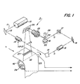
- Scanner 5 is provided with an illumination source, which in the exemplary arrangement shown comprises a laser 10 for generating a collimated beam 11 of monochromatic radiation.
- illumination source which in the exemplary arrangement shown comprises a laser 10 for generating a collimated beam 11 of monochromatic radiation.
- beam 11 is modulated by modulator 14 in conformance with image information (DATA) contained in video image signals input thereto. Beam 11 is reflected by mirror 12 to modulator 14.
- DATA image information
- Modulator 14 may be any suitable electro optical modulator for imparting video information to beam 11.
- the modulator 14 may be for example, a Pockel's cell comprising a potassium dihydrogen phosphate crystal, whose index of refraction is periodically varied by the application of the varying voltage which represents the image signals.
- the image signals which may impart information either by means of binary pulse code modulation or wideband frequency code modulation, represent discrete picture elements and are referred to as pixels herein.
- solid state diode lasers which incorporate both light source and modulator in one unitary structure, may be used in place of the separate laser/modulator arrangement shown.
- the beam 11 Downstream of modulator 14, the beam 11 is reflected by mirror 13 to an astigmatic lens configuration 15 which focuses the beam 11 to a controlled energy distribution, i.e. a spot onto at least one facet 20 of a suitable beam scanning element, illustrated herein by rotating polygon 18.
- Mirrors 16, 17 cooperate to direct the beam so that the beam impinges onto facets 20 of polygon 18.
- the rotational axis of polygon 18 is orthogonal to the plane in which beam 11 travels.
- Facets 20 of polygon 18 are mirrored surfaces suitable for reflecting any radiated beam impinging thereon.
- scanning may be effected by any other suitable device such as mirrored piezoelectric crystals, planar reflecting mirrors, and the like.
- a lens 22 is located in the optical path between the polygon 18 and the imaging member which in the exemplary arrangement shown, comprises a photoconductive belt 25 of a xerographic reproduction or copying system (not shown).
- the lens 22 is of a diameter suitable to focus the beam reflected from facets 20 of the rotating polygon 18 to a spot in a focal plane proximate the surface of belt 25.
- Mirror 26 guides the beam 11 onto belt 25.
- imaging member is shown herein as a photoconductive belt, other types of'imaging members such as a drum, web, etc. may be conte mplated.
- Lens 22 provides a linear relationship between the rotating polygon 18 and the deflection of the spot in the traverse direction at the belt 25. This linearization by optical means prevents barrel or pincushion- type distortion effects without the need for electrical compensation.
- Polygon 18 is preferably driven by a hysteresis synchronous motor 28 through drive shaft 29 with the rotational velocity or speed of polygon 18 synchronized with the velocity or speed of photoconductive belt 25, as will appear.
- a cylindrical lens 27 is interposed between mirror 26 and belt 25 to compensate for any misalignment of the optical elements.
- the rotating polygon 18 scans or sweeps the beam 11 across the photoconductive surface of belt 25 (in the X-direction shown in the drawings), beam 11 tracing a scan line 32 on the photoconductive surface of belt 25.
- Photodetectors 38, 39 provided adjacent the surface of belt 25 and astride the path of the scanning beam generate a pulse each time beam 11 sweeps across the photoconductive surface to establish Start of Scan (SOS) and End of Scan (EOS) signals respectively.
- SOS Start of Scan
- EOS End of Scan
- the width of the SOS-EOS pulse generated by photodetectors 38, 39 (termed LINE SYNC herein) is dependent upon the velocity at which polygon 18 rotates. Variations in polygon velocity, due for example, to the hunting characteristics of motor 28, cause a change in the width of the LINE SYNC pulse generated by detectors 38, 39.
- photoconductive belt 25 is supported internally by rolls 40, 41, 42, roll 40 being drivingly coupled to a suitable belt drive motor 43.
- One or more timing marks 52 which may for example comprise holes, cutouts, transparent sections or the like are provided in belt 25, preferably along one edge thereof and outside the imaging area.
- a suitable sensor 53 such as a photodetector and cooperating light source 54 are suitably mounted on opposing sides of belt 25 opposite the path of movement of timing marks 52.
- a signal pulse is generated by sensor 53 each time a timing mark 52 passes between sensor 53 and light source 54.
- the train of signal pulses produced by sensor 53 are input to microprocessor 56 via lead 55.
- energization of belt drive motor 43 moves photoconductive belt 25 consecutively through a series of xerographic processing stations (not shown). These include a charging station whereat a uniform electrostatic charge is applied to the photoconductive surface of belt 25 and an exposure station where imaging beam 11 modulated by modulator 14 and scanned by rotating polygon 18, sweeps across the belt surface (in the X-direction) to selectively discharge the charged photoconductive surface in accordance with the content of the image pixels input to modulator 14.
- the latent electrostatic image formed on belt 25 thereafter passes through a developing station whereat the image is rendered visible by the application of toner.
- the developed image is carried on belt 25 to a transfer station where the developed image is transferred to a copy substrate material, typically a sheet of paper.
- a fusing device thereafter fixes the transferred image on the copy paper to provide a permanent copy.
- the photoconductive surface of belt 25 is cleaned by a suitable cleaning device such as a rotating brush.
- a suitable cleaning device such as a rotating brush.
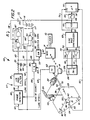
- image pixels (DATA) in the form of digital signals are provided through an 8 bit data bus 45 from a suitable source (not shown).
- bus 45 is coupled to parallel in-serial out shift register 46, the serial output of shift register 46 being coupled to the input gate of modulator 14 through lead 47.
- Shift register 46 is driven by pixel clock pulses derived from clock 49 through lead 59.
- the SOS and EOS pulses generated by photodetectors 38, 39 respectively are output through leads 50, 51, to flip flop 62.
- the LINE SYNC pulse output by flip flop 62 is fed through lead 63 to clock 49 to control the clock operating cycle, as will appear.
- a predetermined velocity or speed relationship is required between the imaging member, here photoconductive belt 25, and the scanning element (i.e. polygon 18) if images of desired size and resolution are to be produced.
- this relationship is upset by a change in the velocity of photoconductive belt 25, image distortions may result since it is understood that the velocity of belt 25, which moves in a direction (the Y-direction) normal to the direction of scanning beam 11 (the X-direction) is determinative of the spacing between successive scan lines.
- scanners of the aforedescribed type have suffered from an inability to compensate for variations in the velocity of the imaging member (i.e. belt 25) without manual intervention by a trained technician having specialized test and calibration equipment at his disposal.
- the present invention is intended to provide a control system which effectively maintains the aforementioned velocity relationship between imaging member and scanning element in cases where the velocity of the imaging member undergoes a change, without the need for manual correction or adjustment.
- the train of signal pulses output by sensor 53 is fed to Micro Processor (UP) 56, it being understood that the period or frequency of the signal pulse train generated by sensor 53 is determined by the speed or velocity of photoconductive belt 25.
- Micro Processor 56 which is programmed to generate a control signal proportional to the sensed velocity of belt 25, outputs a digital control signal in lead 58 to digital-to- analog (D/A) converter 64 which converts the digital control signal to an analog control signal.
- D/A digital-to- analog
- a Voltage Controlled Oscillator (VCO) 65 provides the energizing source for polygon drive motor 28.
- the control signal output of D/A converter 64 is input to the frequency control gate of VCO 65 through lead 66, the control signal from D/A converter 64 serving to control the frequency of the motor energizing signal output by VCO 65.
- the signal output of VCO 65 is fed through lead 68 to a digital sine wave synthesizer 69 which serves to generate sine and cosine power waves in leads 70, 71 respectively.
- the sine and cosine waves output by synthesizer 69 are amplified by linear amplifiers 74, 75 of motor drive circuit 73, and coupled to the field windings 77, 78 of polygon drive motor 28 through motor leads 60, 61.
- the signal output of VCO 65 is fed back to Micro Processor 56 via feedback loop 79.
- Micro processor 56 compares the frequency of the signal output of VCO 65, which represents polygon velocity, with desired polygon velocity as represented by the frequency of the signal pulses output by belt sensor 53. Where a difference exists, the level of the control signal output of Micro Processor 56 to VCO 65 is adjusted to change the frequency of the motor energizing signal output of VCO 65 to adjust polygon velocity and maintain the aforementioned velocity relationship between belt 25 and polygon 18.
- belt drive motor 43 is energized to move photoconductive belt 25.
- laser 10 and polygon drive motor 28 are energized, the latter serving to rotate polygon 18 and scan the beam 11 output by laser 10 across the previously charged surface of the moving photoconductive belt 25.
- Image pixels (DATA) are clocked into register 46 through data bus 45 by means of pixel clock signals generated by the clock 49, the image pixels being output from register 46 through lead 47 to modulator 14. As described, modulator 14 modulates the beam 11 in accordance with the content of the image pixels input thereto.
- sensor 53 With movement of belt 25, sensor 53 generates a pulse-like signal as timing marks 52 on the photoconductive belt 25 move therepast, the frequency of the signal pulses generated by sensor 53 being proportional to the velocity of belt 25.
- the signal pulses output by belt sensor 53 are fed to Micro Processor 56 which in turn generates a control signal proportional to the velocity of belt 25.
- the digital control signal output of micro processor 56 is converted to an analog signal by D/A converter 64 and used to set the frequency of the motor energizing signal output of VCO 65.
- the signal output of VCO 65 is converted to sine and cosine wave form by synthesizer 69, amplified by motor drive circuit 73, and input to windings 77, 78 of polygon motor 28 to operate motor 28 and rotate polygon 18 as described heretofore.
- Feedback loop 79 feeds back the motor energizing signals output of VCO 65 to Micro Processor 56 where the frequency of the motor signal is compared with the frequency of the signal pulses output by belt sensor 53, the latter representing the current velocity of photoconductive belt 25.
- a change in the frequency of the signal pulses output by belt sensor 53, reflecting a change in the velocity of belt 25, results in a difference between the frequency of the motor energizing signals output by VCO 65 and the frequency of the signal pulses output by belt sensor 53. There results a corresponding change in the level of the control signal output of Micro Processor 56 to VCO 65 which changes the frequency setting of VCO 65. This results in a change in the frequency of the motor energizing signal output of VCO 65 with corresponding change in the speed of polygon drive motor 28 and polygon 18. The aforedescribed process continues until such time as the frequency of the motor energizing signal output of VCO 65 again equals the frequency of the signal pulses output by belt sensor 53, indicating desired synchronization between polygon and photoconductive belt velocities.
- clock 49 includes a highly stable Voltage Controlled Oscillator (VCO) 81 for generating pixel clock pulses, together with a servo control loop 57 for synchronizing the frequency of the pixel clock pulses output by VCO 81 with the scanning velocity of beam 11.
- VCO 81 has an inverting logic output gate 90 and input delay device 94, the latter being comprised of a pair of series coupled non-inverting gates 96, 97.
- the output side of delay device 94 is coupled to one input of gate 90 through lead 95.
- Clock pulses output by gate 90 are fed via clock output lead 59 to shift register 46.
- the LINE SYNC signal output of flip flop 62 which serves to enable clock output gate 90, is coupled to one input of gate 90 through leads 63, 92.
- Clock return lead 93 which is coupled between clock output lead 59 and the input lead 83 to delay device 94, provides a clock feedback loop.
- clock signal output to clock output lead 59 is fed back as described above and following a delay imposed by delay device 94 and gate 90, resets gate 90 to switch the signal output of gate 90 from high to low.
- the aforedescribed process generates in clock output lead 59 a pulse-like signal or clock output which serves to clock image pixels to modulator 14.
- the enabling signal (LINE SYNC) to gate 90 of VCO 81 goes low to terminate the output of pixel clock pulses to clock output lead 59.
- Servo control loop 57 has a divide-by-N register 82 preset to a count representing the pixel clock frequency required to produce a desired image resolution. Pixel clock pulses output by VCO 81 to clock output lead 59 are input to register 82 through lead 85.
- the signal output of register 82 termed END OF COUNT, is fed through lead 86 to one input of phase detector 84.
- the LINE SYNC signal output of flip flop 62 is fed via lead 63 to a second input of phase detector 84.
- phase detector 84 produces a signal in output lead 88 thereof, with a strength proportional to the phase relationship between the LINE SYNC and, END OF COUNT signal pulses input thereto.
- Output lead 88 of phase detector 84 is coupled through low pass filter 89 and blocking capacitor 101 to the input lead 83 of VCO 81.
- Filter 89 serves to filter out high frequency transients in the detector output while capacitor 101 provides D. C. blocking.
- a series coupled capacitor/diode 98, 99 are provided upstream of blocking capacitor 101 to permit voltage tuning of the frequency of VCO 81 through control over the rise and fall times of gate 90.
- register 82 is preset to the current image resolution expressed for example in pixels per scan line by means of control lead 103.
- Pixel clock pulses generated by VCO 81 are input to register 82 where the pixel clock pulses are, in effect, compared with desired image resolution (i.e. the number of pixels in the scan line) represented by the count to which register 82 is preset.
- desired image resolution i.e. the number of pixels in the scan line
- the END OF COUNT signal output by register 82 undergoes a change.
- the END OF COUNT signal output of register 82 is fed to phase detector 84 where, in effect, the pulse width of the END OF COUNT signal is compared with the pulse width of the LINE SYNC signal generated by SOS and EOS detectors 38, 39 respectively. Where the signals (END OF COUNT and LINE SYNC) are in phase, the signal output of phase detector 84 is zero and no change in the frequency of the pixel clock signals output by VCO 81 occurs.
- the pulse width of the LINE SYNC signal decreases.
- the pulse width of the LINE SYNC signal increases.
- phase detector 84 On a change in the pulse width of the LINE SYNC signal, phase detector 84 generates a control signal having a potential proportional to the degree of change.
- the control signal changes the setting of capacitor/diode 98, 99 thereby causing either an increase or decrease in the output rise and fall times of clock output gate 90 depending on the control signal change.
- the frequency of the pixel clock signals output by VCO 81 is changed in accommodation of the change in beam scanning velocity.
- Control circuit 115 is provided for automatically changing the center or mid-point frequency of pixel clock 49 in response to a change in the control signal output of Micro Processor 56.
- Control circuit 115 comprises a varactor type circuit having capacitor/diode pair 116, 117 respectively coupled between lead 118 and ground.
- Lead 118 is coupled between output lead 66 of D/A converter 64 and gates 96, 97 of delay device 94.
- Capacitor 120 in lead 118 provides D. C. blocking.
- microprocessor 56 may be dispensed with and another control arrangement employed to control the velocity of scanning polygon 18 in accordance with changes in the velocity of photoconductive belt 25.
- a servo loop control incorporating a divide-by-N circuit to reduce the frequency of the signal output of VCO 65 in feed back loop 79 and a phase detector for comparing the signal output of belt sensor 53 with the reduced frequency signal output of VCO 65 in feedback loop 79 and controlling the frequency of the signal output of VCO 65 in response thereto may instead be contemplated.
- a low pass filter may be provided in the phase detector output to remove high frequency transients.
Landscapes
- Engineering & Computer Science (AREA)
- Multimedia (AREA)
- Signal Processing (AREA)
- Facsimile Scanning Arrangements (AREA)
- Mechanical Optical Scanning Systems (AREA)
- Laser Beam Printer (AREA)
Abstract
Description
- This invention relates to raster output scanners, and more particularly to apparatus and method for maintaining constant image size despite variations in the velocity of the member on which images are produced.
- Raster output scanning systems typically consist of a scanner and xerographic apparatus, images being created through exposure of the previously charged xerographic apparatus photoconductive member by the scanner's scanning beam modulated in accordance with video image signals or pixels. Heretofore, to maintain image size uniform in the direction of movement of the photoconductive member, (i.e. the Y-direction) manual adjustment of the scanner has been required. For example, where a two- phase hysteresis synchronous motor was used to drive the scanning polygon and a quadrature oscillator to provide sine and cosine power waves to the motor, correlation between polygon velocity and photoconductive member velocity for constant image size could be achieved by the rather difficult and time consuming expediency of adjusting the oscillator's potentiometer while monitoring the distance between adjoining lines of a test document.
- On the other hand, image size in the direction of scan (i.e. the X-direction) is known to be a function of image signal or pixel rate which in turn is determined by the image signal or pixel clock frequency. A clock with phase locked loop control may for example, be used to generate pixel clock pulses at a frequency which is a function of polygon velocity, the phase locked loop monitoring variations in polygon velocity and adjusting clock frequency to maintain image size constant in the aforesaid beam scan direction.
- However, the voltage controlled oscillators normally required in systems of this type have limited range and when the adjustment limit is exceeded which is often the case, manual adjustment to restore linear tracking of the polygon velocity is necessary. Again, this typically required the use of a special test document with measurements taken therefrom used as a basis for adjusting the pixel clock frequency.
- While the foregoing arrangements for adjusting the scanner components to accommodate wear and assure uniform image size over the scanner lifetime may be used effectively, both require manual implementation and periodic institution. Because of the high degree of training and skill required, as well as the special tools and instruments needed, these procedures are relatively expensive and impose delays during which scanner operation must be curtailed.
- From one aspect the invention provides a raster output scanner for producing images on a movable imaging member in response to image pixels input thereto, said scanner including means for generating a high intensity imaging beam, a movable scanning element for scanning said beam across said imaging member, means for driving said scanning element, modulator means for modulating said beam to selectively expose said imaging member in accordance with image pixels input thereto, and clock means for generating pixel clock pulses for clocking image pixels to said modulator means, characterized by sensor means for producing a pulse-like signal representative of the velocity of said imaging member; and control means responsive to said signal for adjusting the speed of said drive means to change the velocity of said scanning element to thereby maintain a predetermined velocity relationship between said imaging member and said scanning element in spite of changes in the velocity of said imaging member during operation of said scanner.
- From another aspect, the invention provides a method of providing constant image size in a raster output scanner despite changes in velocity of the imaging member on which images are produced, said scanner including a high intensity imaging beam, a movable scan element for scanning said beam across said member a drive means for driving said scan element, modulator means for modulating said beam in accordance with image signals input thereto to generate an image representative of said image signals on said member, and clock means for generating clock pulses for clocking image signals to said modulator means, characterized by the steps of generating a pulse-like signal representative of the velocity of said imaging member; and adjusting the speed of said drive means in accordance with said signal to maintain a predetermined velocity relationship between said scan element and said imaging member so that image size remains constant despite changes in the velocity of said imaging member.
- In order that the invention may be more readily understood, reference will now be made to the accompanying drawings, in which:-
- Figure 1 is an isometric view of an exemplary raster output scanner with which the present invention may be used; and
- Figure 2 is a schematic view illustrating the control system of the present invention.
- Referring to Figures 1 and 2, there is shown an exemplary
raster output scanner 5 with which the present invention is adapted for use.Scanner 5 is provided with an illumination source, which in the exemplary arrangement shown comprises alaser 10 for generating a collimated beam 11 of monochromatic radiation. In the exemplary arrangement shown, beam 11 is modulated bymodulator 14 in conformance with image information (DATA) contained in video image signals input thereto. Beam 11 is reflected bymirror 12 tomodulator 14. -
Modulator 14 may be any suitable electro optical modulator for imparting video information to beam 11. Themodulator 14 may be for example, a Pockel's cell comprising a potassium dihydrogen phosphate crystal, whose index of refraction is periodically varied by the application of the varying voltage which represents the image signals. The image signals, which may impart information either by means of binary pulse code modulation or wideband frequency code modulation, represent discrete picture elements and are referred to as pixels herein. - It is understood that solid state diode lasers, which incorporate both light source and modulator in one unitary structure, may be used in place of the separate laser/modulator arrangement shown.
- Downstream of
modulator 14, the beam 11 is reflected bymirror 13 to anastigmatic lens configuration 15 which focuses the beam 11 to a controlled energy distribution, i.e. a spot onto at least onefacet 20 of a suitable beam scanning element, illustrated herein by rotatingpolygon 18.Mirrors 16, 17 cooperate to direct the beam so that the beam impinges ontofacets 20 ofpolygon 18. - In the preferred embodiment, the rotational axis of
polygon 18 is orthogonal to the plane in which beam 11 travels.Facets 20 ofpolygon 18 are mirrored surfaces suitable for reflecting any radiated beam impinging thereon. Alternately, scanning may be effected by any other suitable device such as mirrored piezoelectric crystals, planar reflecting mirrors, and the like. - A
lens 22 is located in the optical path between thepolygon 18 and the imaging member which in the exemplary arrangement shown, comprises aphotoconductive belt 25 of a xerographic reproduction or copying system (not shown). Thelens 22 is of a diameter suitable to focus the beam reflected fromfacets 20 of the rotatingpolygon 18 to a spot in a focal plane proximate the surface ofbelt 25.Mirror 26 guides the beam 11 ontobelt 25. - While the imaging member is shown herein as a photoconductive belt, other types of'imaging members such as a drum, web, etc. may be conte mplated.
-
Lens 22 provides a linear relationship between the rotatingpolygon 18 and the deflection of the spot in the traverse direction at thebelt 25. This linearization by optical means prevents barrel or pincushion- type distortion effects without the need for electrical compensation. - Polygon 18 is preferably driven by a hysteresis
synchronous motor 28 through drive shaft 29 with the rotational velocity or speed ofpolygon 18 synchronized with the velocity or speed ofphotoconductive belt 25, as will appear. Preferably, acylindrical lens 27 is interposed betweenmirror 26 andbelt 25 to compensate for any misalignment of the optical elements. - During operation of
scanner 5, the rotatingpolygon 18 scans or sweeps the beam 11 across the photoconductive surface of belt 25 (in the X-direction shown in the drawings), beam 11 tracing ascan line 32 on the photoconductive surface ofbelt 25.Photodetectors belt 25 and astride the path of the scanning beam generate a pulse each time beam 11 sweeps across the photoconductive surface to establish Start of Scan (SOS) and End of Scan (EOS) signals respectively. As will be understood, the width of the SOS-EOS pulse generated byphotodetectors 38, 39 (termed LINE SYNC herein) is dependent upon the velocity at whichpolygon 18 rotates. Variations in polygon velocity, due for example, to the hunting characteristics ofmotor 28, cause a change in the width of the LINE SYNC pulse generated bydetectors - In the exemplary arrangement shown,
photoconductive belt 25 is supported internally byrolls belt drive motor 43. One ormore timing marks 52, which may for example comprise holes, cutouts, transparent sections or the like are provided inbelt 25, preferably along one edge thereof and outside the imaging area. Asuitable sensor 53, such as a photodetector and cooperatinglight source 54 are suitably mounted on opposing sides ofbelt 25 opposite the path of movement oftiming marks 52. As will be understood, a signal pulse is generated bysensor 53 each time atiming mark 52 passes betweensensor 53 andlight source 54. The train of signal pulses produced bysensor 53 are input tomicroprocessor 56 vialead 55. - As will be understood by those skilled in the xerographic arts, energization of
belt drive motor 43 movesphotoconductive belt 25 consecutively through a series of xerographic processing stations (not shown). These include a charging station whereat a uniform electrostatic charge is applied to the photoconductive surface ofbelt 25 and an exposure station where imaging beam 11 modulated bymodulator 14 and scanned by rotatingpolygon 18, sweeps across the belt surface (in the X-direction) to selectively discharge the charged photoconductive surface in accordance with the content of the image pixels input tomodulator 14. The latent electrostatic image formed onbelt 25 thereafter passes through a developing station whereat the image is rendered visible by the application of toner. Following development, the developed image is carried onbelt 25 to a transfer station where the developed image is transferred to a copy substrate material, typically a sheet of paper. A fusing device thereafter fixes the transferred image on the copy paper to provide a permanent copy. - Following transfer, the photoconductive surface of
belt 25 is cleaned by a suitable cleaning device such as a rotating brush. The aforedescribed cycle is repeated for subsequent or additional copies. - Referring particularly to Figure 2, image pixels (DATA) in the form of digital signals are provided through an 8
bit data bus 45 from a suitable source (not shown). In the example shown,bus 45 is coupled to parallel in-serial outshift register 46, the serial output ofshift register 46 being coupled to the input gate ofmodulator 14 throughlead 47.Shift register 46 is driven by pixel clock pulses derived fromclock 49 throughlead 59. - The SOS and EOS pulses generated by
photodetectors leads flop 62. The LINE SYNC pulse output byflip flop 62 is fed through lead 63 toclock 49 to control the clock operating cycle, as will appear. - As will be understood, a predetermined velocity or speed relationship is required between the imaging member, here
photoconductive belt 25, and the scanning element (i.e. polygon 18) if images of desired size and resolution are to be produced. Where this relationship is upset by a change in the velocity ofphotoconductive belt 25, image distortions may result since it is understood that the velocity ofbelt 25, which moves in a direction (the Y-direction) normal to the direction of scanning beam 11 (the X-direction) is determinative of the spacing between successive scan lines. Heretofore, scanners of the aforedescribed type have suffered from an inability to compensate for variations in the velocity of the imaging member (i.e. belt 25) without manual intervention by a trained technician having specialized test and calibration equipment at his disposal. The present invention is intended to provide a control system which effectively maintains the aforementioned velocity relationship between imaging member and scanning element in cases where the velocity of the imaging member undergoes a change, without the need for manual correction or adjustment. - Referring to Figure 2, the train of signal pulses output by
sensor 53 is fed to Micro Processor (UP) 56, it being understood that the period or frequency of the signal pulse train generated bysensor 53 is determined by the speed or velocity ofphotoconductive belt 25. MicroProcessor 56, which is programmed to generate a control signal proportional to the sensed velocity ofbelt 25, outputs a digital control signal in lead 58 to digital-to- analog (D/A)converter 64 which converts the digital control signal to an analog control signal. - A Voltage Controlled Oscillator (VCO) 65 provides the energizing source for
polygon drive motor 28. The control signal output of D/A converter 64 is input to the frequency control gate ofVCO 65 throughlead 66, the control signal from D/A converter 64 serving to control the frequency of the motor energizing signal output byVCO 65. The signal output ofVCO 65 is fed throughlead 68 to a digital sine wave synthesizer 69 which serves to generate sine and cosine power waves inleads 70, 71 respectively. The sine and cosine waves output by synthesizer 69 are amplified bylinear amplifiers motor drive circuit 73, and coupled to thefield windings polygon drive motor 28 through motor leads 60, 61. - The signal output of
VCO 65 is fed back toMicro Processor 56 viafeedback loop 79.Micro processor 56 compares the frequency of the signal output ofVCO 65, which represents polygon velocity, with desired polygon velocity as represented by the frequency of the signal pulses output bybelt sensor 53. Where a difference exists, the level of the control signal output ofMicro Processor 56 toVCO 65 is adjusted to change the frequency of the motor energizing signal output ofVCO 65 to adjust polygon velocity and maintain the aforementioned velocity relationship betweenbelt 25 andpolygon 18. - During operation of
scanner 5,belt drive motor 43 is energized to movephotoconductive belt 25. At the same time,laser 10 andpolygon drive motor 28 are energized, the latter serving to rotatepolygon 18 and scan the beam 11 output bylaser 10 across the previously charged surface of the movingphotoconductive belt 25. Image pixels (DATA) are clocked intoregister 46 throughdata bus 45 by means of pixel clock signals generated by theclock 49, the image pixels being output fromregister 46 throughlead 47 tomodulator 14. As described,modulator 14 modulates the beam 11 in accordance with the content of the image pixels input thereto. - With movement of
belt 25,sensor 53 generates a pulse-like signal as timing marks 52 on thephotoconductive belt 25 move therepast, the frequency of the signal pulses generated bysensor 53 being proportional to the velocity ofbelt 25. The signal pulses output bybelt sensor 53 are fed toMicro Processor 56 which in turn generates a control signal proportional to the velocity ofbelt 25. The digital control signal output ofmicro processor 56 is converted to an analog signal by D/A converter 64 and used to set the frequency of the motor energizing signal output ofVCO 65. The signal output ofVCO 65 is converted to sine and cosine wave form by synthesizer 69, amplified bymotor drive circuit 73, and input towindings polygon motor 28 to operatemotor 28 and rotatepolygon 18 as described heretofore.Feedback loop 79 feeds back the motor energizing signals output ofVCO 65 toMicro Processor 56 where the frequency of the motor signal is compared with the frequency of the signal pulses output bybelt sensor 53, the latter representing the current velocity ofphotoconductive belt 25. - A change in the frequency of the signal pulses output by
belt sensor 53, reflecting a change in the velocity ofbelt 25, results in a difference between the frequency of the motor energizing signals output byVCO 65 and the frequency of the signal pulses output bybelt sensor 53. There results a corresponding change in the level of the control signal output ofMicro Processor 56 toVCO 65 which changes the frequency setting ofVCO 65. This results in a change in the frequency of the motor energizing signal output ofVCO 65 with corresponding change in the speed ofpolygon drive motor 28 andpolygon 18. The aforedescribed process continues until such time as the frequency of the motor energizing signal output ofVCO 65 again equals the frequency of the signal pulses output bybelt sensor 53, indicating desired synchronization between polygon and photoconductive belt velocities. - Referring to Figure 2,
clock 49 includes a highly stable Voltage Controlled Oscillator (VCO) 81 for generating pixel clock pulses, together with aservo control loop 57 for synchronizing the frequency of the pixel clock pulses output by VCO 81 with the scanning velocity of beam 11. VCO 81 has an invertinglogic output gate 90 andinput delay device 94, the latter being comprised of a pair of series couplednon-inverting gates delay device 94 is coupled to one input ofgate 90 throughlead 95. Clock pulses output bygate 90 are fed viaclock output lead 59 to shiftregister 46. - The LINE SYNC signal output of
flip flop 62, which serves to enableclock output gate 90, is coupled to one input ofgate 90 throughleads 63, 92.Clock return lead 93, which is coupled betweenclock output lead 59 and theinput lead 83 to delaydevice 94, provides a clock feedback loop. - In operation of the
clock 49, on the enabling signal (LINE SYNC) inlead 92 going high for example, the output ofgate 90 toclock output lead 59, after a delay interval inherent ingate 90, goes low. The clock signal inlead 59 is fed back vialead 93 andclock input lead 83 togate 96 ofdelay device 94. There the return signal is successively delayed bygates gates lead 95, after the delay characteristic ofgate 90, triggersgate 90, causing the signal output ofgate 90 to lead 59 to go high. The clock signal output toclock output lead 59 is fed back as described above and following a delay imposed bydelay device 94 andgate 90, resetsgate 90 to switch the signal output ofgate 90 from high to low. As a result, the aforedescribed process generates in clock output lead 59 a pulse-like signal or clock output which serves to clock image pixels tomodulator 14. - At the end of the scan line as determined by
EOS detector 39, the enabling signal (LINE SYNC) togate 90 of VCO 81 goes low to terminate the output of pixel clock pulses toclock output lead 59. -
Servo control loop 57 has a divide-by-N register 82 preset to a count representing the pixel clock frequency required to produce a desired image resolution. Pixel clock pulses output by VCO 81 toclock output lead 59 are input to register 82 throughlead 85. The signal output ofregister 82, termed END OF COUNT, is fed through lead 86 to one input ofphase detector 84. The LINE SYNC signal output offlip flop 62 is fed via lead 63 to a second input ofphase detector 84. As will be understood,phase detector 84 produces a signal inoutput lead 88 thereof, with a strength proportional to the phase relationship between the LINE SYNC and, END OF COUNT signal pulses input thereto. -
Output lead 88 ofphase detector 84 is coupled throughlow pass filter 89 and blocking capacitor 101 to theinput lead 83 of VCO 81.Filter 89 serves to filter out high frequency transients in the detector output while capacitor 101 provides D. C. blocking. A series coupled capacitor/diode gate 90. - In operation, register 82 is preset to the current image resolution expressed for example in pixels per scan line by means of
control lead 103. Pixel clock pulses generated by VCO 81 are input to register 82 where the pixel clock pulses are, in effect, compared with desired image resolution (i.e. the number of pixels in the scan line) represented by the count to which register 82 is preset. On attaining coincidence, the END OF COUNT signal output byregister 82 undergoes a change. - The END OF COUNT signal output of
register 82 is fed to phasedetector 84 where, in effect, the pulse width of the END OF COUNT signal is compared with the pulse width of the LINE SYNC signal generated by SOS andEOS detectors phase detector 84 is zero and no change in the frequency of the pixel clock signals output by VCO 81 occurs. - Should the scanning velocity of beam 11 change as for example, to accommodate a change in the velocity of
photoconductive belt 25 as described heretofore, the pulse width of the LINE SYNC signal generated by SOS andEOS detectors photoconductive belt 25, the pulse width of the LINE SYNC signal decreases. Where the scanning velocity of. beam 11 is decreased in accommodation of a decrease in belt velocity, the pulse width of the LINE SYNC signal increases. - On a change in the pulse width of the LINE SYNC signal,
phase detector 84 generates a control signal having a potential proportional to the degree of change. The control signal changes the setting of capacitor/diode clock output gate 90 depending on the control signal change. As a result, the frequency of the pixel clock signals output by VCO 81 is changed in accommodation of the change in beam scanning velocity. - Inasmuch as changes in the velocity of
photoconductive belt 25 over a period may exceed the limits of adjustment ofclock 49, acontrol circuit 115 is provided for automatically changing the center or mid-point frequency ofpixel clock 49 in response to a change in the control signal output ofMicro Processor 56.Control circuit 115 comprises a varactor type circuit having capacitor/diode pair lead 118 and ground.Lead 118 is coupled betweenoutput lead 66 of D/A converter 64 andgates delay device 94.Capacitor 120 inlead 118 provides D. C. blocking. - In operation, changes in the control signal output by
micro processor 56 in response to changes in velocity of thephotoconductive belt 25, changes the operating potential ondelay device 94. As a result, the center or mid-point frequency of VCO 81, and henceclock 49, is shifted, the direction and degree of shift being dependent upon the change in control signal potential, which in turn reflects the change in photoconductive belt velocity. - As will be apparent to those skilled in the art,
microprocessor 56 may be dispensed with and another control arrangement employed to control the velocity ofscanning polygon 18 in accordance with changes in the velocity ofphotoconductive belt 25. For example, a servo loop control incorporating a divide-by-N circuit to reduce the frequency of the signal output ofVCO 65 in feed backloop 79 and a phase detector for comparing the signal output ofbelt sensor 53 with the reduced frequency signal output ofVCO 65 infeedback loop 79 and controlling the frequency of the signal output ofVCO 65 in response thereto may instead be contemplated. As in the clockservo control loop 57 discussed above, a low pass filter may be provided in the phase detector output to remove high frequency transients. - It will further be understood that whatever the control arrangement employed, consideration may have to be given to initial or standing start conditions if start up and acceleration up to speed of
photoconductive belt 25 are to be accommodated in cases where only a single or minimum number of timing marks 52 are provided onbelt 25. It is appreciated that the fewer the number of timing marks onbelt 25, the less representative the initial velocity signals generated bysensor 53 are and hence the more difficult to obtain an accurate representation of belt velocity at startup. - While the invention has been described with reference to the structure disclosed, it is not confined to the details set forth, but is intended to cover such modifications or changes as may come within the scope of the following claims:
Claims (9)
said first mentioned control means (56) including means (115) to shift said preset frequency range in response to changes in said imaging member velocity.
Applications Claiming Priority (2)
| Application Number | Priority Date | Filing Date | Title |
|---|---|---|---|
| US229811 | 1981-01-30 | ||
| US06/229,811 US4349847A (en) | 1981-01-30 | 1981-01-30 | Image size control for raster scanners |
Publications (4)
| Publication Number | Publication Date |
|---|---|
| EP0057586A2 true EP0057586A2 (en) | 1982-08-11 |
| EP0057586A3 EP0057586A3 (en) | 1982-12-15 |
| EP0057586B1 EP0057586B1 (en) | 1985-11-06 |
| EP0057586B2 EP0057586B2 (en) | 1989-07-12 |
Family
ID=22862763
Family Applications (1)
| Application Number | Title | Priority Date | Filing Date |
|---|---|---|---|
| EP82300463A Expired EP0057586B2 (en) | 1981-01-30 | 1982-01-29 | Raster output scanner and method |
Country Status (5)
| Country | Link |
|---|---|
| US (1) | US4349847A (en) |
| EP (1) | EP0057586B2 (en) |
| JP (1) | JPS57143982A (en) |
| CA (1) | CA1169913A (en) |
| DE (1) | DE3267209D1 (en) |
Cited By (3)
| Publication number | Priority date | Publication date | Assignee | Title |
|---|---|---|---|---|
| EP0535783A1 (en) * | 1991-08-28 | 1993-04-07 | Xerox Corporation | Method and apparatus for reducing pixel clock jitter in a laser scanner |
| EP0647013A1 (en) * | 1993-10-05 | 1995-04-05 | Bayer Corporation | A method and apparatus for synchronizing system operations using a programmable element |
| GB2304199A (en) * | 1993-09-07 | 1997-03-12 | Gerber Systems Corp | Creating a pixel clock for a scanner |
Families Citing this family (17)
| Publication number | Priority date | Publication date | Assignee | Title |
|---|---|---|---|---|
| JPS6058774A (en) * | 1983-09-09 | 1985-04-04 | Fuji Photo Film Co Ltd | Synchronizing signal generating circuit |
| DE3419288A1 (en) * | 1984-05-23 | 1985-11-28 | Mergenthaler Linotype Gmbh, 6236 Eschborn | METHOD AND DEVICE FOR SYNCHRONIZING A MATERIAL RAIL, IN PARTICULAR PHOTOSENSITIVE MATERIAL RAIL IN A PHOTO SETTING METHOD |
| US4639789A (en) * | 1984-05-29 | 1987-01-27 | Xerox Corporation | Raster scanner variable-frequency clock circuit |
| US4622593A (en) * | 1984-05-29 | 1986-11-11 | Xerox Corporation | Polygon signature correction |
| JPS61161869A (en) * | 1985-01-11 | 1986-07-22 | Dainippon Screen Mfg Co Ltd | Method and device for generating picture element synchronizing signal in picture input scanning device and reproduced record scanning device |
| US4760251A (en) * | 1985-07-31 | 1988-07-26 | Ricoh Company, Ltd. | Optical scanning apparatus wherein image scanning clock signal frequency is corrected to render scanning speed constant |
| US4694156A (en) * | 1986-02-14 | 1987-09-15 | Xerox Corporation | Pixel placement sensing arrangement using split detecting elements |
| JPH0795155B2 (en) * | 1987-09-18 | 1995-10-11 | 富士写真フイルム株式会社 | Optical scanning device synchronization circuit |
| US5043744A (en) * | 1990-05-18 | 1991-08-27 | Xerox Corporation | Raster scanner including scanning beam tilt correction |
| US5241252A (en) * | 1991-05-15 | 1993-08-31 | Xerox Corporation | Motor drive system for a polygon scanner |
| US5212570A (en) * | 1991-06-27 | 1993-05-18 | Xerox Corporation | Pixel clock phase locked loop for a laser scanner |
| US5204694A (en) * | 1991-07-29 | 1993-04-20 | Xerox Corporation | Ros printer incorporating a variable wavelength laser |
| US5153644A (en) * | 1991-08-19 | 1992-10-06 | Xerox Corporation | Dual mode correction of image distortion in a xerographic printing apparatus |
| US5386123A (en) * | 1992-08-20 | 1995-01-31 | Xerox Corporation | Beam steering sensor for a raster scanner using a lateral effect detecting device |
| JP3658026B2 (en) * | 1995-01-27 | 2005-06-08 | キヤノン株式会社 | Image processing device |
| US5991470A (en) * | 1995-06-07 | 1999-11-23 | Computer Identics, Inc. | One-dimensional scanner system for two-dimensional image acquisition |
| US5821970A (en) * | 1995-07-28 | 1998-10-13 | Ricoh Company, Ltd. | Color image forming apparatus |
Family Cites Families (11)
| Publication number | Priority date | Publication date | Assignee | Title |
|---|---|---|---|---|
| US3835249A (en) * | 1972-12-26 | 1974-09-10 | Ibm | Scanning light synchronization system |
| US4028732A (en) * | 1973-03-02 | 1977-06-07 | Lucien Salter | Apparatus and method for display of images |
| US3848087A (en) * | 1973-10-29 | 1974-11-12 | Rca Corp | Optical scanner control system |
| DE2413034C3 (en) * | 1974-03-19 | 1983-11-17 | Dr.-Ing. Rudolf Hell Gmbh, 2300 Kiel | Method and arrangement for avoiding errors in the reproduction of original images |
| US4002829A (en) * | 1974-08-29 | 1977-01-11 | W. R. Grace & Co. | Autosynchronous optical scanning and recording laser system with fiber optic light detection |
| US4000368A (en) * | 1975-08-04 | 1976-12-28 | Dacom, Inc. | Nonuniform clock generator for document reproduction apparatus |
| US4140903A (en) * | 1977-01-03 | 1979-02-20 | Xerox Corporation | Precision speed control for optical scanners |
| US4130838A (en) * | 1977-08-11 | 1978-12-19 | Xerox Corporation | Speed control apparatus for scanning system |
| US4180822A (en) * | 1978-04-13 | 1979-12-25 | Rca Corporation | Optical scanner and recorder |
| US4268867A (en) * | 1979-06-29 | 1981-05-19 | Xerox Corporation | Pixel clock for scanner |
| JPS5794711A (en) * | 1980-12-04 | 1982-06-12 | Canon Inc | Optical scanner |
-
1981
- 1981-01-30 US US06/229,811 patent/US4349847A/en not_active Expired - Lifetime
- 1981-12-08 CA CA000391758A patent/CA1169913A/en not_active Expired
-
1982
- 1982-01-28 JP JP57012501A patent/JPS57143982A/en active Granted
- 1982-01-29 EP EP82300463A patent/EP0057586B2/en not_active Expired
- 1982-01-29 DE DE8282300463T patent/DE3267209D1/en not_active Expired
Cited By (5)
| Publication number | Priority date | Publication date | Assignee | Title |
|---|---|---|---|---|
| EP0535783A1 (en) * | 1991-08-28 | 1993-04-07 | Xerox Corporation | Method and apparatus for reducing pixel clock jitter in a laser scanner |
| GB2304199A (en) * | 1993-09-07 | 1997-03-12 | Gerber Systems Corp | Creating a pixel clock for a scanner |
| GB2304199B (en) * | 1993-09-07 | 1997-11-05 | Gerber Systems Corp | Apparatus and method of creating a pixel clock for a scanner |
| EP0647013A1 (en) * | 1993-10-05 | 1995-04-05 | Bayer Corporation | A method and apparatus for synchronizing system operations using a programmable element |
| US5486745A (en) * | 1993-10-05 | 1996-01-23 | Miles Inc. | Method and apparatus for synchronizing system operations using a programmable element |
Also Published As
| Publication number | Publication date |
|---|---|
| EP0057586B1 (en) | 1985-11-06 |
| EP0057586B2 (en) | 1989-07-12 |
| US4349847A (en) | 1982-09-14 |
| JPS57143982A (en) | 1982-09-06 |
| JPH0532734B2 (en) | 1993-05-17 |
| EP0057586A3 (en) | 1982-12-15 |
| DE3267209D1 (en) | 1985-12-12 |
| CA1169913A (en) | 1984-06-26 |
Similar Documents
| Publication | Publication Date | Title |
|---|---|---|
| US4349847A (en) | Image size control for raster scanners | |
| US4268867A (en) | Pixel clock for scanner | |
| US5175570A (en) | Color image forming apparatus having an adjustor which corrects the position of a latent image according to registration marks | |
| US5381165A (en) | Raster output scanner with process direction registration | |
| US6133932A (en) | Method and apparatus for adjusting a line synchronization signal in response to photoreceptor motion | |
| EP0581083B1 (en) | Error reduction methods in scanning systems | |
| US4807156A (en) | Adjustable print size control for raster output scanners | |
| US4801978A (en) | Image bar printer compensated for vibration-generated scan line errors | |
| US4216378A (en) | Optical scanner | |
| US5287125A (en) | Raster output scanner with process direction spot position control | |
| US5517230A (en) | Control system for a variable-resolution raster output scanner | |
| EP0816943B1 (en) | Image registration system and method | |
| US5530642A (en) | Control system for aspect ratio and magnification of a raster output scanner | |
| GB2040511A (en) | Light scanning | |
| US6219085B1 (en) | Method and system for improved performance of adjustable printer clocks in an electrophotographic device | |
| EP0435640A2 (en) | Color image forming apparatus | |
| EP0535783B1 (en) | Method and apparatus for reducing pixel clock jitter in a laser scanner | |
| EP0589654B1 (en) | Device and apparatus for scan line process direction control in a multicolor electrostatographic machine | |
| EP0589651B1 (en) | Optical device having an electrically variable refractive index for scan line skew correction in electrostatographic printing machines | |
| US6355926B1 (en) | Raster output scanner beam steering | |
| US6351277B1 (en) | Direct digital synthesis pixel clock generator | |
| JPS6157749B2 (en) | ||
| US6278109B1 (en) | Facet tracking using wavelength variations and a dispersive element | |
| EP0514160B1 (en) | Programmable motor drive system for a polygon scanner | |
| US5241252A (en) | Motor drive system for a polygon scanner |
Legal Events
| Date | Code | Title | Description |
|---|---|---|---|
| PUAI | Public reference made under article 153(3) epc to a published international application that has entered the european phase |
Free format text: ORIGINAL CODE: 0009012 |
|
| AK | Designated contracting states |
Designated state(s): DE FR GB |
|
| PUAL | Search report despatched |
Free format text: ORIGINAL CODE: 0009013 |
|
| AK | Designated contracting states |
Designated state(s): DE FR GB |
|
| 17P | Request for examination filed |
Effective date: 19830609 |
|
| GRAA | (expected) grant |
Free format text: ORIGINAL CODE: 0009210 |
|
| AK | Designated contracting states |
Designated state(s): DE FR GB |
|
| ET | Fr: translation filed | ||
| REF | Corresponds to: |
Ref document number: 3267209 Country of ref document: DE Date of ref document: 19851212 |
|
| PLBI | Opposition filed |
Free format text: ORIGINAL CODE: 0009260 |
|
| PLBI | Opposition filed |
Free format text: ORIGINAL CODE: 0009260 |
|
| 26 | Opposition filed |
Opponent name: OCE-NEDERLAND B.V. Effective date: 19860630 |
|
| 26 | Opposition filed |
Opponent name: DR.-ING. RUDOLF HELL GMBH Effective date: 19860805 |
|
| PUAH | Patent maintained in amended form |
Free format text: ORIGINAL CODE: 0009272 |
|
| STAA | Information on the status of an ep patent application or granted ep patent |
Free format text: STATUS: PATENT MAINTAINED AS AMENDED |
|
| 27A | Patent maintained in amended form |
Effective date: 19890712 |
|
| AK | Designated contracting states |
Kind code of ref document: B2 Designated state(s): DE FR GB |
|
| ET3 | Fr: translation filed ** decision concerning opposition | ||
| PGFP | Annual fee paid to national office [announced via postgrant information from national office to epo] |
Ref country code: FR Payment date: 19990111 Year of fee payment: 18 |
|
| PGFP | Annual fee paid to national office [announced via postgrant information from national office to epo] |
Ref country code: GB Payment date: 19990128 Year of fee payment: 18 |
|
| PGFP | Annual fee paid to national office [announced via postgrant information from national office to epo] |
Ref country code: DE Payment date: 19990205 Year of fee payment: 18 |
|
| PG25 | Lapsed in a contracting state [announced via postgrant information from national office to epo] |
Ref country code: GB Free format text: LAPSE BECAUSE OF NON-PAYMENT OF DUE FEES Effective date: 20000129 |
|
| GBPC | Gb: european patent ceased through non-payment of renewal fee |
Effective date: 20000129 |
|
| PG25 | Lapsed in a contracting state [announced via postgrant information from national office to epo] |
Ref country code: FR Free format text: LAPSE BECAUSE OF NON-PAYMENT OF DUE FEES Effective date: 20000929 |
|
| PG25 | Lapsed in a contracting state [announced via postgrant information from national office to epo] |
Ref country code: DE Free format text: LAPSE BECAUSE OF NON-PAYMENT OF DUE FEES Effective date: 20001101 |
|
| REG | Reference to a national code |
Ref country code: FR Ref legal event code: ST |