EP0057275A2 - Système de mémoire de données digitales - Google Patents
Système de mémoire de données digitales Download PDFInfo
- Publication number
- EP0057275A2 EP0057275A2 EP81110076A EP81110076A EP0057275A2 EP 0057275 A2 EP0057275 A2 EP 0057275A2 EP 81110076 A EP81110076 A EP 81110076A EP 81110076 A EP81110076 A EP 81110076A EP 0057275 A2 EP0057275 A2 EP 0057275A2
- Authority
- EP
- European Patent Office
- Prior art keywords
- controller
- port switch
- switch
- decoder
- status register
- Prior art date
- Legal status (The legal status is an assumption and is not a legal conclusion. Google has not performed a legal analysis and makes no representation as to the accuracy of the status listed.)
- Granted
Links
Images


Classifications
-
- G—PHYSICS
- G06—COMPUTING; CALCULATING OR COUNTING
- G06F—ELECTRIC DIGITAL DATA PROCESSING
- G06F13/00—Interconnection of, or transfer of information or other signals between, memories, input/output devices or central processing units
-
- G—PHYSICS
- G06—COMPUTING; CALCULATING OR COUNTING
- G06F—ELECTRIC DIGITAL DATA PROCESSING
- G06F13/00—Interconnection of, or transfer of information or other signals between, memories, input/output devices or central processing units
- G06F13/38—Information transfer, e.g. on bus
- G06F13/40—Bus structure
- G06F13/4004—Coupling between buses
- G06F13/4022—Coupling between buses using switching circuits, e.g. switching matrix, connection or expansion network
-
- G—PHYSICS
- G06—COMPUTING; CALCULATING OR COUNTING
- G06F—ELECTRIC DIGITAL DATA PROCESSING
- G06F11/00—Error detection; Error correction; Monitoring
- G06F11/07—Responding to the occurrence of a fault, e.g. fault tolerance
- G06F11/16—Error detection or correction of the data by redundancy in hardware
- G06F11/20—Error detection or correction of the data by redundancy in hardware using active fault-masking, e.g. by switching out faulty elements or by switching in spare elements
- G06F11/2053—Error detection or correction of the data by redundancy in hardware using active fault-masking, e.g. by switching out faulty elements or by switching in spare elements where persistent mass storage functionality or persistent mass storage control functionality is redundant
- G06F11/2089—Redundant storage control functionality
-
- G—PHYSICS
- G06—COMPUTING; CALCULATING OR COUNTING
- G06F—ELECTRIC DIGITAL DATA PROCESSING
- G06F3/00—Input arrangements for transferring data to be processed into a form capable of being handled by the computer; Output arrangements for transferring data from processing unit to output unit, e.g. interface arrangements
- G06F3/06—Digital input from, or digital output to, record carriers, e.g. RAID, emulated record carriers or networked record carriers
- G06F3/0601—Interfaces specially adapted for storage systems
- G06F3/0628—Interfaces specially adapted for storage systems making use of a particular technique
- G06F3/0655—Vertical data movement, i.e. input-output transfer; data movement between one or more hosts and one or more storage devices
- G06F3/0658—Controller construction arrangements
Definitions
- This invention relates to digital data storage systems having storage devices accessible through two separate paths. More specifically, the invention involves sharing data stored in a string of devices which are individually addressable from either one of a pair of controllers that are supplied with address selection signals from two separate control units associated with different data processing systems.
- a storage device or a string of storage devices is connected to the CPU through a control unit and a channel. If the switching arrangement which permits sharing involves switching the input of the control unit between a pair of channels, the arrangement is generally referred to as a "two channel switch.” If the switching arrangement involves switching the string of storage devices between a pair of control units, the arrangement.is generally referred to in the art as a "string switch.”
- the prior art also discloses, in U. S. Patent 4,207,609, a data processing system in which a plurality of disk files are shared by a plurality of central processing units.
- a plurality of separate paths are possible between each addressable storage device and each CPU through the control unit and the channels.
- the switching arrangement disclosed therein is such that the states of the segments of each possible path is stored so that when an interconnection is desired between a CPU and a storage device, reference to the stored states of the various path segments permits a path to be established whenever there are free segments between existing switching nodes of the system.
- the disclosed switching arrangement has been referred to in the art as "dynamic pathing" in that the state of the various path segments are dynamically mapped.
- the arrangement in most applications enhances the system performance and permits greater availability of the shared data relative to the string switch and two channel switch arrangements. This is because with the string switch arrangement, the entire string appears busywhen one device in the string is selected. In the "dynamic pathing" arrangement, the non-selected devices in the string are addressable by the second controller even though one device has been selected by the first controller; hence, the resulting increase in the availability of stored data.
- the cost of dynamically mapping the state of the various path segments in terms of actual hardware, programming cost, and system performance in continually updating the map, cannot be justified for all data processing applications.
- a switching arrangement which is less costly but provides access to other devices on the string when one device is busy is, therefore, desirable.
- a digital data storage system comprising a plurality of storage devices and first and second device controllers each connectable to a data processing system through a first interface and to any of said plurality of devices through a second interface in response to a command from such data processing system, the system being characterised by a plurality of subchannels, each of which includes first and second port switches associated respectively with said first and second controllers, interlocking means interconnecting said switches, and bus means connecting said first and second device controllers to at least one of said storage devices through said first and second port switches, each port switch being operable in response to a connection request command from its associated controller identifying one of said storage devices to effect such connection provided the identified device is available and to cause said interlocking means to prevent the port switch associated with the other controller from responding to a request connection command for the device so connected.
- the system shown in FIG. 1 corresponds generally to the system disclosed in U. S. Patent 4,207,609 which permits data stored on devices 0 through 3 to be shared by three separate CPU's.
- the illustrated configuration of CPU' S , channels and control units is a typical IBM-type 360/370 system configuration.
- the connection of the string of storage devices 0 through 3 to each control unit represents the "dynamic pathing" approach to this shared storage arrangement referred to earlier in connection with prior art systems.
- the interface between control unit I and the controller is referred to in the art as the CTLI Interface, the details of which may be found in the IBM 3370 Product Attachment Information Manual.
- the interface between the controller and the devices is referred to in the art as the File Controller Interface or FCI.
- one of the devices 0 through 3 is selected when one of the CPU's issues a start I/O command to an associated channel which, in turn, issues a Channel Command Word or CCW to its associated control unit.
- the CCW contains the device address to be selected so that the control unit, in turn, issues a series of its commands which, when interpreted by the controller, selects the addressed device for connection to the control unit.
- the path established by a selection sequence involves the CTLI interface from the control unit to the controller and the FCI interface from the controller to the device.
- the devices 0 through 3 are connected by a parallel set of FCI interfaces from each controller. In configurations not provided with "dynamic pathing", the devices may be "daisy-chained" to the controller. In either situation, the serial data channel for transferring the data between a device and the controller is separate from the FCI.
- the read data is decoded in the controller and converted into parallel form. Also in the controller, the write data is encoded and serialized for each device.
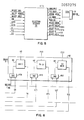
- FIG. 2 illustrates in block diagram form a storage subsystem embodying the present invention.
- the storage subsystem comprises a pair of controllers 10 and 10' which are connected, for example, to control unit I and control unit II of the system shown in FIG. 1 through respective CTLI interfaces.
- the system further includes four storage subchannels 0 through 3.
- Each subchannel includes a storage device and a pair of port switches PS and PS', each of which functions generally to connect the storage device of the subchannel to its associated controller 10 or 10'.
- an interlock line ITL extends between the port switches PS and PS'. The function of the interlock line is to prevent both switches from being closed at any one time.
- the general function of the port switch is to connect the FCI interface cable from its associated controller to the device in response to a Select Request signal which is provided by the controller.
- the Select Request signal is provided by the controller along with the device address received from the control unit. Operation of the port switch in response to a Select Request signal connects the device to the controller and interlocks the other port switch of the channel so that it cannot respond to a Select Request signal for the device from the other controller.
- FIG. 3 illustrates schematically one of the port switches PS shown in FIG. 2.
- the switch comprises a switch control box SWC having an input to which the Select Request line is connected; two interlock output lines which are sent to the other switch PS' to prevent its operation when the Select Request line closes switch PS; and two other input lines from the port switch PS' corresponding to the interlock lines from the switch PS.
- the switch control logic block functions to connect the FCI interface from the controller 10 to the device and to a status logic block STA.
- the status logic block provides status data to the FCI interface as to the status of certain aspects of the subchannel and/or the storage device, such as if the subchannel is busy or has been assigned or reserved to one of the controllers.
- the status of the switch PS may be set from either controller, as will be seen in FIG. 4 which is a detailed logic diagram of the various logical components associated with one of the subchannels.
- the CTLI interface between the control unit and controller comprises a number of different buses and control lines.
- the FCI interface between the controller and device comprises buses and control lines. Commands and control parameters are generally provided to the device on an 8-bit bus referred to as Device Bus Out. Status information is provided to the controller from the device on an 8- bit bus referred to as Device Bus In.
- a Tag Bus extends from the controller to the device which defines generally the type of data that exists on Bus Out. A number of other lines are used to deskew signals in each of the devices, to acknowledge and request service, and to maintain selection of the device once it has been obtained.
- the concept of the present invention involves viewing each port switch as a device from the standpoint of addressing during a selection sequence, i.e., the port switch is addressed as if it were a storage device. If the addressed port switch is not busy, the associated device is automatically connected when the switch closes, and the other port switch is locked out.
- the port switch may include status registers or latches similar to those in the device, such as an Assignment Latch, a CE Mode Latch, and a Pack Change Latch, etc.
- the status latches in each switch are set and reset by tag commands from the controllers.
- the switch, if addressed by the controller may therefore, appear busy if, for example, the device has been reserved or assigned to the other switch or the device has been placed in the CE Mode for servicing.
- the Pack Change Latches in each switch will be serviced by the respective controllers and reset, thereby advising the respective CPU's that the device is back on-line.
- the storage subsystem shown in FIG. 2 in addition to providing greater availability of the data stored on the shared device, also permits the logic of each port switch to be controlled by an alternate path through another subchannel. For example, if one of the switches associated with the device of subchannel 0 becomes inoperative in that commands to the device cannot be transmitted through the switch, then unique commands may be sent through a switch associated with another subchannel and then to the device of the channel having the defective switch. Such an arrangement improves the overall reliability of the storage system and the availability of data.
- FIG. 4 The preferred embodiment of the present invention is shown in detail in FIG. 4 in which device N is connectable to either controller through the port switches which are implemented, as shown, in digital logic.
- the FCI interface from each controller includes Bus Out 100, Tag Bus 101 which includes the tag gate line for deskewing signals on the Tag Bus, Bus In 102, and Select Bus 103.
- Select Request line 104 a Select Hold line 105 and an Atten- tion/Response line 106 complete the interface lines from each of the controllers.
- Each port switch comprises generally a Selection Decoder 120, a Tag Decoder 130, and a Status Register 140.
- the port switch includes a plurality of logical AND-gates for selectively connecting interface lines to the device N and to the components 120, 130 and 140 of the port switch.
- Bus Out 100 from each controller is connected to its associated Status Register 140 and device N through AND-gates 150 and 151, respectively.
- Tag Bus 101 for each controller is connected to the Tag Decoder 130 through AND-gate 153 and to the device N through AND-gate 154.
- Bus In 102 is developed from one of three possible AND-gates 156 through 158.
- the output of device N is connected through AND-gate 159 and AND-gate 157.
- the output of Selection Decoder 120 is connected to AND-gate 156, while an output 139 of the Status Register 140 is connected to AND-gate 158.
- Selection Decoder 120 as shown in FIG.
- the Selection Decoder 120 has three inputs from the controller 10, namely one line 103 from Select Bus, the Select Request line 104 which is not part of the standard FCI interface, and the Select Hold line 105.
- the Selection Decoder 120 also receives two interlock output lines SRB' and SFB' from the Selection Decoder 120' associated with the other port switch PSO'.
- Selection Decoder 120 as shown in FIG. 4, also has three inputs from the Status Register 140, namely Device Assigned, CE Mode, and Pack Change status signal lines.
- Selection Decoder 120 functions to logically combine in a straightforward, logical manner selected ones of the above described input signals to provide, first, a group of control signals for controlling the various gates and, secondly, a group of status signals which are supplied to Bus In 102 through AND-gate 156.
- FIG. 5 shows the various input and output lines of the Selection Decoder.
- the signals supplied to Bus In through AND-gate 156, as shown in FIG. 5, comprise the following signals:
- the FCI Busy signal results from operation of the other switch having control of the interface lines to the device N.
- a Select Error signal is provided merely to reflect an error condition in the switch and operates as an alert to the selecting controller.
- the remaining output signals, SHA, SFA, SRA and SO are generated primarily in response to the three input signals from the controller, and are used primarily as enabling signals to the various logical AND-gates.
- the Select Request input signal will be decoded as the Select Request signal SRA, provided the Select Bus has the appropriate bit significant address matching the address of the port switch and the interlock from the other switch is not active.
- a Select Request Latch is set to provide the SRA signal.
- a similar Select SFA Latch is set, the output of which provides the SFA signal that is employed as the interlock signal for the other port switch PSO'.
- the Select Hold A signal SHA is developed by gating the Select Hold input signal with the output of the SFA latch. Select Hold A and Select Request A are used to control whether commands on Bus Out 100 and Tag Bus 101 are gated to the Tag Decoder 130 and Status Register 140, or to the corresponding registers in device N.
- the port switch is selected first by raising Select Request 104 with the appropriate address on the Select Bus 103. If the switch is available, the available status is returned on Bus In 102 and the switch is captured. Select Hold 105 is then raised, in which case command and tag data from the controller will be sent directly to the device N rather than to the switch. Command and tag data from the controller is sent to the Status Register 140 and Tag Decoder 130 by dropping Select Hold 105 and maintaining Select Request 104 active. Deselection of device N occurs when Select Hold 105 is dropped.
- F IG. 6 shows the details of the Status Register 140.
- the register comprises three separate latches 141, 142 and 143, designated respectively the Assignment Latch, the Pack Change Latch, and the CE Mode Latch.
- the latches are set through AND-gates 145A, B, and C, each of which is supplied with a different predetermined line of Bus Out and set signals SA, SPC and SCE from the Tag Decoders 130.
- the latches 141, 142 and 143 are reset from the output of the Tag Decoder 130.
- the Assignment Latch 141 associated with the port switch PSO, is set by the command on Bus Out 100 from the controller 10' and a tag on Tag Bus 101, that also is sent from the controller 10' through PSO' to Tag Decoder 130. Stated differently, the state of the Assignment Latch 141 associated with port switch 0 indirectly reflects a Not Available status to its associated controller since the latch is really set and reset under the control of the other controller.
- the CE Mode Latch is set from either controller and reflects a Busy or Not Available status of the device to both controllers 10 and 10'. It is also reset from either controller.
- the Pack Change Latch associated with controller 10, is set from commands and tags from controller 10'. However, the Pack Change Latch is reset by commands and tag decodes from controller 10.
- the state of the Pack Change Latch indicates to the system that the device has recently been brought back on-line.
- the Pack Change Latch is set by the other controller 10' and reset by its associated controller 10.
- the FCI interface buses and lines to the switch originate from registers of the output port of the controller.
- the FCI interface lines from the switch terminate at funnels of the input port.
- Device selection normally involves the controller placing an 8-bit byte on the Select Bus 103 where each bit position is an address of one device to be selected, placing a Select Tag on the Tag Bus 101 and placing an all zero byte on Bus Out 100.
- the controller 10 then raises the Select Request line 104 to initiate the actual selection process. Assuming the port switch PSO is available, raising the Select Request line 104 causes the Select Decoder 120 to raise the output line SRA and the output control line SFA. This causes the interlocking of the port switch PSO' associated with the other controller 10' so that it cannot connect to the device N.
- the status of Bus In 102' to controller 10' indicates that the device is busy to controller 10' and inhibits the gating of Bus Out 101' and Tag Bus 101', to switch PSO'.
- controller 10 in response to sensing the switch on Bus In 102, activates Select Hold.
- Controller 10 then interacts with the device N as if the port switch PSO was not involved, i.e., communication between the controller and the device are independent of the switch which is also transparent to the rest of the system.
- the Select Hold line 105 is used to. control the transfer of further commands from the controller 10 to the Status Registers 140 and 140' and to the Tag Decoders 130 and 130'. Commands such as Set Assignment, Set CE Mode, and Set Pack Change Latch are directed to the port switch whenever the Select Hold line 105 is dropped by controller 10 when these commands are issued.
- the set commands for Status Register 140 are sent by controller 10' through port switch PSO'. Reset commands to Status Register 140 are sent from controller 10 through port switch PSO.
- the CE Mode latch for PSO is set from controller 10' and reset by controller 10'.
- the Pack Change Latch for port switch PSO is set from controller 10' and reset from controller 10.
- the Unconditional Release Tag is decoded by the Tag Decoder 103 of the port switch in one channel and supplied to the Status Register 140 of the port switch in an adjacent channel via line 200 to reset the Assignment Latch.
- This Unconditional Release command is a safeguard which permits access to a device in the event one port switch becomes inoperable after setting the Assignment Latch, preventing the other controller from accessing the device.
- controllers 10 and 10' are not shown in detail in that various controllers known in the art may be employed.
- the microcontroller disclosed and claimed in U. S. Serial No. 921,147, filed June 30, 1978 and assigned to the assignee of the present invention (assignee's docket number SA978035A), may be advantageously employed to interconnect the devices 0 through 3 to an IBM-type 3880 control unit in the manner shown in the drawings.
- each controller is provided with four separate ports.
- Each of the four subchannels shown in FIG. 2, as shown, is provided with one addressable device. It will be obvious to those skilled in the art that, while only one device is shown associated with each channel, the device may, in practice, have two separate independently addressable file portions, such as exists in the IBM-type 3370 and 3375 disk files. In such an arrangement, each port switch will include the necessary status latches and controls to reflect the status of each addressable device.
Applications Claiming Priority (2)
| Application Number | Priority Date | Filing Date | Title |
|---|---|---|---|
| US230937 | 1981-02-02 | ||
| US06/230,937 US4381543A (en) | 1981-02-02 | 1981-02-02 | Controller port switch arrangement for sharing stored data among different systems |
Publications (3)
| Publication Number | Publication Date |
|---|---|
| EP0057275A2 true EP0057275A2 (fr) | 1982-08-11 |
| EP0057275A3 EP0057275A3 (en) | 1982-09-01 |
| EP0057275B1 EP0057275B1 (fr) | 1987-11-11 |
Family
ID=22867141
Family Applications (1)
| Application Number | Title | Priority Date | Filing Date |
|---|---|---|---|
| EP81110076A Expired EP0057275B1 (fr) | 1981-02-02 | 1981-12-02 | Système de mémoire de données digitales |
Country Status (7)
| Country | Link |
|---|---|
| US (1) | US4381543A (fr) |
| EP (1) | EP0057275B1 (fr) |
| JP (1) | JPS57130160A (fr) |
| KR (1) | KR860001435B1 (fr) |
| BR (1) | BR8200484A (fr) |
| DE (1) | DE3176525D1 (fr) |
| PH (1) | PH20084A (fr) |
Cited By (3)
| Publication number | Priority date | Publication date | Assignee | Title |
|---|---|---|---|---|
| GB2301464A (en) * | 1995-05-19 | 1996-12-04 | Compaq Computer Corp | Multi-server fault tolerance using in-band signalling |
| US5822512A (en) * | 1995-05-19 | 1998-10-13 | Compaq Computer Corporartion | Switching control in a fault tolerant system |
| US6032271A (en) * | 1996-06-05 | 2000-02-29 | Compaq Computer Corporation | Method and apparatus for identifying faulty devices in a computer system |
Families Citing this family (10)
| Publication number | Priority date | Publication date | Assignee | Title |
|---|---|---|---|---|
| US4794520A (en) * | 1987-03-30 | 1988-12-27 | C-Guard Laboratories, Inc. | Interface system for computer port sharing of multiple devices |
| JPH01320564A (ja) * | 1988-06-23 | 1989-12-26 | Hitachi Ltd | 並列処理装置 |
| AU650242B2 (en) * | 1989-11-28 | 1994-06-16 | International Business Machines Corporation | Methods and apparatus for dynamically managing input/output (I/O) connectivity |
| US5398331A (en) * | 1992-07-08 | 1995-03-14 | International Business Machines Corporation | Shared storage controller for dual copy shared data |
| US6338110B1 (en) * | 1997-11-14 | 2002-01-08 | Sun Microsystems, Inc. | Partitioning of storage channels using programmable switches |
| US6144994A (en) * | 1998-06-25 | 2000-11-07 | Lucent Technologies Inc. | Interface for flexible address bandwidth allocation |
| US6434634B1 (en) * | 1999-01-06 | 2002-08-13 | C-Media Electronics Inc. | Method and apparatus adaptable to a standard game port of a personal computer for interfacing an external HSP modem, a joystick and a MIDI interface |
| DE19923879A1 (de) * | 1999-05-25 | 2000-11-30 | Bosch Gmbh Robert | Steuergerät |
| US6625747B1 (en) * | 2000-06-30 | 2003-09-23 | Dell Products L.P. | Computer storage system and failover method |
| CN104461386A (zh) * | 2014-12-01 | 2015-03-25 | 北京同有飞骥科技股份有限公司 | 一种基于龙芯处理器的双控磁盘阵列 |
Citations (2)
| Publication number | Priority date | Publication date | Assignee | Title |
|---|---|---|---|---|
| US4007448A (en) * | 1974-08-15 | 1977-02-08 | Digital Equipment Corporation | Drive for connection to multiple controllers in a digital data secondary storage facility |
| US4207609A (en) * | 1978-05-08 | 1980-06-10 | International Business Machines Corporation | Method and means for path independent device reservation and reconnection in a multi-CPU and shared device access system |
Family Cites Families (3)
| Publication number | Priority date | Publication date | Assignee | Title |
|---|---|---|---|---|
| US4253144A (en) * | 1978-12-21 | 1981-02-24 | Burroughs Corporation | Multi-processor communication network |
| US4253146A (en) * | 1978-12-21 | 1981-02-24 | Burroughs Corporation | Module for coupling computer-processors |
| US4276609A (en) * | 1979-01-04 | 1981-06-30 | Ncr Corporation | CCD memory retrieval system |
-
1981
- 1981-02-02 US US06/230,937 patent/US4381543A/en not_active Expired - Lifetime
- 1981-12-02 DE DE8181110076T patent/DE3176525D1/de not_active Expired
- 1981-12-02 EP EP81110076A patent/EP0057275B1/fr not_active Expired
- 1981-12-18 JP JP56203795A patent/JPS57130160A/ja active Granted
- 1981-12-28 KR KR8105166A patent/KR860001435B1/ko active
-
1982
- 1982-01-14 PH PH26737A patent/PH20084A/en unknown
- 1982-01-29 BR BR8200484A patent/BR8200484A/pt not_active IP Right Cessation
Patent Citations (2)
| Publication number | Priority date | Publication date | Assignee | Title |
|---|---|---|---|---|
| US4007448A (en) * | 1974-08-15 | 1977-02-08 | Digital Equipment Corporation | Drive for connection to multiple controllers in a digital data secondary storage facility |
| US4207609A (en) * | 1978-05-08 | 1980-06-10 | International Business Machines Corporation | Method and means for path independent device reservation and reconnection in a multi-CPU and shared device access system |
Non-Patent Citations (4)
| Title |
|---|
| COMPUTER DESIGN, vol. 11, no. 11, November 1972, pages 107-114, Concord (USA); * |
| IBM TECHNICAL DISCLOSURE BULLETIN, vol. 18, no. 2, July 1975, page 548, New York (USA); * |
| IBM TECHNICAL DISCLOSURE BULLETIN, vol. 19, no. 8, January 1977, pages 3219-3221, New York (USA); * |
| IBM TECHNICAL DISCLOSURE BULLETIN, vol. 22, no. 1, June 1979, pages 342-344, New York (USA); * |
Cited By (4)
| Publication number | Priority date | Publication date | Assignee | Title |
|---|---|---|---|---|
| GB2301464A (en) * | 1995-05-19 | 1996-12-04 | Compaq Computer Corp | Multi-server fault tolerance using in-band signalling |
| US5822512A (en) * | 1995-05-19 | 1998-10-13 | Compaq Computer Corporartion | Switching control in a fault tolerant system |
| GB2301464B (en) * | 1995-05-19 | 2000-04-26 | Compaq Computer Corp | Multi-server fault tolerance using in-band signalling |
| US6032271A (en) * | 1996-06-05 | 2000-02-29 | Compaq Computer Corporation | Method and apparatus for identifying faulty devices in a computer system |
Also Published As
| Publication number | Publication date |
|---|---|
| DE3176525D1 (en) | 1987-12-17 |
| EP0057275A3 (en) | 1982-09-01 |
| KR830008244A (ko) | 1983-11-16 |
| KR860001435B1 (en) | 1986-09-24 |
| JPH033253B2 (fr) | 1991-01-18 |
| PH20084A (en) | 1986-09-24 |
| JPS57130160A (en) | 1982-08-12 |
| EP0057275B1 (fr) | 1987-11-11 |
| BR8200484A (pt) | 1982-11-30 |
| US4381543A (en) | 1983-04-26 |
Similar Documents
| Publication | Publication Date | Title |
|---|---|---|
| US5812782A (en) | Host central processors with associated controller to capture a selected one of a number of memory units via path control commands | |
| US4964038A (en) | Data processing system having automatic address allocation arrangements for addressing interface cards | |
| US3573855A (en) | Computer memory protection | |
| CA1171545A (fr) | Systemes peripheriques utilisant les interconnexions a trajets multiples et les groupements de trajets et d'acces | |
| US4381543A (en) | Controller port switch arrangement for sharing stored data among different systems | |
| EP0046486A2 (fr) | Système de traitement de données | |
| US4415970A (en) | Cache/disk subsystem with load equalization | |
| US4495564A (en) | Multi sub-channel adapter with single status/address register | |
| GB2089076A (en) | Data proccessing system | |
| WO1999026146A1 (fr) | Partitionnement de canaux de stockage a l'aide de commutateurs programmables | |
| US4509115A (en) | Two-port memory controller | |
| US5146605A (en) | Direct control facility for multiprocessor network | |
| US5005172A (en) | Diagnostic system in a data processing system | |
| US5708784A (en) | Dual bus computer architecture utilizing distributed arbitrators and method of using same | |
| JPH06214782A (ja) | プロセッサ制御コード導入システムおよび方法 | |
| US5596727A (en) | Arrangement for expanding the device capacity of a bus | |
| US5367701A (en) | Partitionable data processing system maintaining access to all main storage units after being partitioned | |
| CA2231872A1 (fr) | Gestion de donnees de disque partagees dans un ordinateur double | |
| US5023831A (en) | Intelligent disk drive having configurable controller subsystem providing drive-status information via host-computer expansion bus | |
| US6122723A (en) | Switching multi-initiator SCSI devices to a singular target bus | |
| US5857117A (en) | Apparatus and method for multiplexing integrated device electronics circuitry with an industry standard architecture bus | |
| US4630197A (en) | Anti-mutilation circuit for protecting dynamic memory | |
| JPS638500B2 (fr) | ||
| EP0316251B1 (fr) | Dispositif de controle direct pour réseau multiprocesseur | |
| US7032054B1 (en) | Method and apparatus for increasing the device count on a single ATA bus |
Legal Events
| Date | Code | Title | Description |
|---|---|---|---|
| PUAI | Public reference made under article 153(3) epc to a published international application that has entered the european phase |
Free format text: ORIGINAL CODE: 0009012 |
|
| PUAL | Search report despatched |
Free format text: ORIGINAL CODE: 0009013 |
|
| AK | Designated contracting states |
Designated state(s): DE FR GB IT |
|
| AK | Designated contracting states |
Designated state(s): DE FR GB IT |
|
| 17P | Request for examination filed |
Effective date: 19821220 |
|
| GRAA | (expected) grant |
Free format text: ORIGINAL CODE: 0009210 |
|
| AK | Designated contracting states |
Kind code of ref document: B1 Designated state(s): DE FR GB IT |
|
| REF | Corresponds to: |
Ref document number: 3176525 Country of ref document: DE Date of ref document: 19871217 |
|
| ET | Fr: translation filed | ||
| ITF | It: translation for a ep patent filed |
Owner name: IBM - DR. ARRABITO MICHELANGELO |
|
| PLBE | No opposition filed within time limit |
Free format text: ORIGINAL CODE: 0009261 |
|
| STAA | Information on the status of an ep patent application or granted ep patent |
Free format text: STATUS: NO OPPOSITION FILED WITHIN TIME LIMIT |
|
| 26N | No opposition filed | ||
| ITTA | It: last paid annual fee | ||
| PGFP | Annual fee paid to national office [announced via postgrant information from national office to epo] |
Ref country code: GB Payment date: 19951127 Year of fee payment: 15 |
|
| PGFP | Annual fee paid to national office [announced via postgrant information from national office to epo] |
Ref country code: FR Payment date: 19951128 Year of fee payment: 15 |
|
| PGFP | Annual fee paid to national office [announced via postgrant information from national office to epo] |
Ref country code: DE Payment date: 19951229 Year of fee payment: 15 |
|
| PG25 | Lapsed in a contracting state [announced via postgrant information from national office to epo] |
Ref country code: GB Effective date: 19961202 |
|
| GBPC | Gb: european patent ceased through non-payment of renewal fee |
Effective date: 19961202 |
|
| PG25 | Lapsed in a contracting state [announced via postgrant information from national office to epo] |
Ref country code: FR Effective date: 19970829 |
|
| PG25 | Lapsed in a contracting state [announced via postgrant information from national office to epo] |
Ref country code: DE Effective date: 19970902 |
|
| REG | Reference to a national code |
Ref country code: FR Ref legal event code: ST |