EP0056571A2 - Multi-emitter type npn transistor - Google Patents
Multi-emitter type npn transistor Download PDFInfo
- Publication number
- EP0056571A2 EP0056571A2 EP82100033A EP82100033A EP0056571A2 EP 0056571 A2 EP0056571 A2 EP 0056571A2 EP 82100033 A EP82100033 A EP 82100033A EP 82100033 A EP82100033 A EP 82100033A EP 0056571 A2 EP0056571 A2 EP 0056571A2
- Authority
- EP
- European Patent Office
- Prior art keywords
- emitter
- base
- region
- npn transistor
- type
- Prior art date
- Legal status (The legal status is an assumption and is not a legal conclusion. Google has not performed a legal analysis and makes no representation as to the accuracy of the status listed.)
- Granted
Links
- 238000009413 insulation Methods 0.000 description 8
- 230000003071 parasitic effect Effects 0.000 description 6
- 230000015572 biosynthetic process Effects 0.000 description 5
- 238000002955 isolation Methods 0.000 description 5
- 230000003321 amplification Effects 0.000 description 4
- 238000003199 nucleic acid amplification method Methods 0.000 description 4
- 238000009792 diffusion process Methods 0.000 description 3
- 239000012535 impurity Substances 0.000 description 3
- VYPSYNLAJGMNEJ-UHFFFAOYSA-N silicon dioxide Inorganic materials O=[Si]=O VYPSYNLAJGMNEJ-UHFFFAOYSA-N 0.000 description 3
- 239000000758 substrate Substances 0.000 description 3
- 238000010276 construction Methods 0.000 description 2
- 238000004519 manufacturing process Methods 0.000 description 2
- 239000004065 semiconductor Substances 0.000 description 2
- XUIMIQQOPSSXEZ-UHFFFAOYSA-N Silicon Chemical compound [Si] XUIMIQQOPSSXEZ-UHFFFAOYSA-N 0.000 description 1
- XAGFODPZIPBFFR-UHFFFAOYSA-N aluminium Chemical compound [Al] XAGFODPZIPBFFR-UHFFFAOYSA-N 0.000 description 1
- 229910052782 aluminium Inorganic materials 0.000 description 1
- 230000000694 effects Effects 0.000 description 1
- 238000012986 modification Methods 0.000 description 1
- 230000004048 modification Effects 0.000 description 1
- 229910052710 silicon Inorganic materials 0.000 description 1
- 239000010703 silicon Substances 0.000 description 1
- 235000012239 silicon dioxide Nutrition 0.000 description 1
- 239000000377 silicon dioxide Substances 0.000 description 1
Images


Classifications
-
- H—ELECTRICITY
- H10—SEMICONDUCTOR DEVICES; ELECTRIC SOLID-STATE DEVICES NOT OTHERWISE PROVIDED FOR
- H10D—INORGANIC ELECTRIC SEMICONDUCTOR DEVICES
- H10D62/00—Semiconductor bodies, or regions thereof, of devices having potential barriers
- H10D62/10—Shapes, relative sizes or dispositions of the regions of the semiconductor bodies; Shapes of the semiconductor bodies
- H10D62/13—Semiconductor regions connected to electrodes carrying current to be rectified, amplified or switched, e.g. source or drain regions
- H10D62/133—Emitter regions of BJTs
- H10D62/135—Non-interconnected multi-emitter structures
-
- H—ELECTRICITY
- H10—SEMICONDUCTOR DEVICES; ELECTRIC SOLID-STATE DEVICES NOT OTHERWISE PROVIDED FOR
- H10D—INORGANIC ELECTRIC SEMICONDUCTOR DEVICES
- H10D48/00—Individual devices not covered by groups H10D1/00 - H10D44/00
- H10D48/30—Devices controlled by electric currents or voltages
- H10D48/32—Devices controlled by only the electric current supplied, or only the electric potential applied, to an electrode which does not carry the current to be rectified, amplified or switched
- H10D48/34—Bipolar devices
- H10D48/345—Bipolar transistors having ohmic electrodes on emitter-like, base-like, and collector-like regions
-
- H—ELECTRICITY
- H10—SEMICONDUCTOR DEVICES; ELECTRIC SOLID-STATE DEVICES NOT OTHERWISE PROVIDED FOR
- H10D—INORGANIC ELECTRIC SEMICONDUCTOR DEVICES
- H10D64/00—Electrodes of devices having potential barriers
- H10D64/20—Electrodes characterised by their shapes, relative sizes or dispositions
- H10D64/27—Electrodes not carrying the current to be rectified, amplified, oscillated or switched, e.g. gates
- H10D64/281—Base electrodes for bipolar transistors
Definitions
- the present invention relates to a multi-emitter type npn transistor.
- a multi-emitter type npn transistor generally has a structure as shown in Figs. 1 and 2.
- the structure as shown in Figs. 1 and 2 there is a problem of the formation of a parasitic lateral npn transistor at a region indicated by the broken line, that is, between the two adjacent emitter regions.
- a conventional npn transistor as shown in Figs.
- 1 and 2 comprises a p-type substrate 2, an n-type epytaxial layer 4 formed on the substrate 2, an n +- type region 6 for collector contact formed in the epytaxial layer 4 by the diffusion of an n-type impurity, a p +- type base region 8 formed in the epytaxial layer 4 by the diffusion of a p-type impurity, emitter regions 10-1 and 10-2 formed in the base region 8 by the diffusion of an n +- type impurity, a p +- type isolation region 11, an insulation film 12 having contact holes of predetermined pattern formed on the major surface of the semiconductor body of this construction, and electrodes 14, 16-1, 16-2 and 18 which are in contact with the regions 6, 10-1, 10-2 and 8 through contact holes formed in the insulation film 12.
- the isolation region 11 and insulation film 12 are omitted in Fig. 1 for simplification. Since the two emitter regions 10-1 and 10-2 are arranged relatively close to each other, the electrons injected to the base region 8 from one emitter region 10-1, for example, reach the other emitter region 10-2, forming a parasitic lateral npn transistor 20 having the emitter region 10-1 as an emitter, the base region 8 as a base, and the emitter region 10-2 as a collector. This parasitic lateral npn transistor affects the original function of the logic circuit formed on the epytaxial layer 4, resulting in erroneous operation of the logic circuit.
- the present invention has been made in consideration of this and has for its object to provide a multi-emitter type npn transistor of a construction so that the formation of an undesirable parasitic lateral npn transistor may be prevented.
- a multi-emitter type npn transistor comprising:
- Figs. 3 and 4 show a multi-emitter type npn transistor according to an embodiment of the present invention.
- an n-type epytaxial layer 24 is formed on a silicon substrate 22 of p conductivity type.
- an n +- type collector contact region 26 In the epytaxial layer 24 are formed an n +- type collector contact region 26, and a p +- type base region 28. Within the p +- type base region 28 are formed two emitter regions 30-1 and 30-2.
- a p +- type region 32 is an isolation region.
- the epytaxial layer 24 defines the collector region.
- An insulation film 34 of, for example, Si0 2 (silicon dioxide) having contact holes of predetermined pattern is formed on the major surface of the semiconductor body of this configuration.
- Electrodes 36, 38-1, 38-2 and 40 of aluminum, for example, are formed in the n +- type collector contact region 26, the n + -type emitter regions 30-1 and 30-2, and the p +- type base region 28 through the contact holes formed in the insulation film 34.
- the isolation region 32 and insulation film 34 are omitted in Fig. 3 for the sake of simplification.
- the contact hole for contact with the base is formed at the position of the midpoint between the emitter regions 30-1 and 30-2.
- a base electrode 40 is formed on the p +- type base region 28 through this base region contact hole. In other words, the base electrode 40 is in contact with the part of the base region 28 which is between the two adjacent emitter regions 30-1 and 30-2.
- the base electrode 40 is connected to an external power supply of positive potential to be kept at a positive potential, and the p-n junction between the p +- type base region 28 and the emitter regions 30-1 and 30-2 is biased in the forward direction. Therefore, most of the electrons injected into the base region 28 from the emitter electrode 38-1 through the emitter region 30-1 are attracted toward the interface between the base region 28 and the base electrode 40 and are recombined with the holes at this interface. As a consequence, the electrons which are injected into the base region 28 from the emitter region 30-1 are prevented from reaching the emitter region 30-2, so that the formation of the parasitic lateral npn transistor of the regions 30-1, 28 and 30-2 is prevented.
- curve I is the characteristic curve for the conventional npn transistor
- curve II is the characteristic curve for the npn transistor of the present invention.
- the ordinate and abscissa in Fig. 5 are both logarithmic scales.
- the distance between the emitters on the mask during the manufacture of the conventional npn transistor of the curve I was set to 40 um, and the distance between the emitters on the mask during the manufacture of the npn transistor of the present invention of the curve II was set'to 30 ⁇ m.
- the distance between the emitters in the npn transistor according to the present invention is set smaller than the distance between the emitter regions of the conventional npn transistor.
- the current amplification 6 of the conventional npn transistor (curve I) is 2 to 4 while the current amplification S of the npn transistor (curve II) of the present invention is about 0.1 in the low current range and is 0.5 to 0.7 even in the high current range. In this way, it is seen that the npn transistor of the present invention shown in Fig. 4 achieves better results than the npn transistor shown in Figs. 1 and 2.
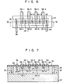
- Figs. 6 and 7 show another embodiment of the present invention, wherein the number of the emitter regions is increased. Since the configuration of the npn transistor of this embodiment is substantially the same except for the emitter regions and the emitter electrodes as the embodiment shown in Figs. 3 and 4, the same reference numerals denote the same parts and the description thereof will be omitted.
- Base region contact holes are formed at the positions of the insulation film which correspond to the emitter regions 30-1, 30-2, 30-3 and 30-4.
- a base electrode 42-1 is in contact with the base region portion between the emitter regions 30-1 and 30-2, base electrode 42-2 is in contact with the base region portion between the emitter regions 30-2 and 30-3.
- a base electrode 42-3 is in contact with the base region portion between the emitter regions 30-3 and 30-4.
- a base electrode 44 is in contact with the base region portion which is not sandwiched between the emitter regions (the right edge of the base region 28 shown in Figs. 6 and 7) through the contact hole.
- the isolation region 32 and insulation film 34 are omitted in Fig. 6.
- the base electrode 44 is for connection with an external power supply (not shown) at positive potential and is connected with such an external power supply during operation.
- the base electrodes 42-1, 42-2 and 42-3 are the electrodes for attracting the electrons. Although these electrodes 42-1, 42-2 and 42-3 are not directly connected to the external power supply, they are electrically connected to the external power supply through the base region 28 since the base electrode 44 is connected to the external power supply to be kept at a positive potential. Therefore, these electrodes 42-1, 42-2 and 42-3 are kept at substantially the same positive potential (potential of the external power supply) as the base electrode 44.
- the electrons injected to the base region 28 from the emitter regions 30-1, 30-2 and 30-3, and 30-4 are attracted to the base electrodes 42-1, 42-2 and 42-3 and the interfaces between these base electrodes and the base region 28 so that these electrons may be recombined with the holes at these interfaces.
- the electrons injected into the base region 28 are prevented from reaching the other emitter regions, so that the formation of lateral npn transistors between the adjacent emitter regions is prevented.
- the base electrodes 42-1, 42-2 and 42-3 are electrically connected to the base electrode 44 for connection with the external power supply through the base region 28, so that the base electrodes are kept at substantially the same potential as the base electrode 44.
- the present invention is not limited to this configuration.
- the layer defining the base electrodes 42-1, 42-2 and 42-3 is extended to form a common connection layer to which an external power supply is connected. In this case, all the base electrodes 42-1, 42-2 and 42-3 are directly connected to the external power supply. In this case, the base electrode 44 for connection with the external power supply in the embodiment shown in Figs. 6 and 7 is not necessary.
- the base electrodes 42-1, 42-2 and 42-3 may be extended and may be connected to the external power supply.
- the base electrodes 42-2 and 42-3 are electrically connected to the base electrode 42-1 through the base region 28, so that the base electrodes 42-2 and 42-3 are kept at substantially the same potential as the base electrode 42-1 (potential of the external power supply).
- the base electrode 44 for connection with the external power supply as in Figs. 6 and 7 need not be formed.
- a base electrode is arranged at the base region portion between two adjacent emitter regions.
- a positive voltage is applied to the base electrode, so that the electrons injected into the base region from one emitter region may be attracted to the interface between the base electrode and the base region to be recombined with the holes at this interface. Therefore, injected electrons are prevented from reaching the other emitter region, and the formation of a parasitic lateral npn transistor may be prevented.
Landscapes
- Bipolar Transistors (AREA)
- Electrodes Of Semiconductors (AREA)
- Bipolar Integrated Circuits (AREA)
Abstract
Description
- The present invention relates to a multi-emitter type npn transistor.
- A multi-emitter type npn transistor generally has a structure as shown in Figs. 1 and 2. However, with the structure as shown in Figs. 1 and 2, there is a problem of the formation of a parasitic lateral npn transistor at a region indicated by the broken line, that is, between the two adjacent emitter regions. Describing this in further detail, a conventional npn transistor, as shown in Figs. 1 and 2, comprises a p-type substrate 2, an n-type
epytaxial layer 4 formed on the substrate 2, an n+-type region 6 for collector contact formed in theepytaxial layer 4 by the diffusion of an n-type impurity, a p+-type base region 8 formed in theepytaxial layer 4 by the diffusion of a p-type impurity, emitter regions 10-1 and 10-2 formed in thebase region 8 by the diffusion of an n+-type impurity, a p+-type isolation region 11, aninsulation film 12 having contact holes of predetermined pattern formed on the major surface of the semiconductor body of this construction, andelectrodes 14, 16-1, 16-2 and 18 which are in contact with theregions 6, 10-1, 10-2 and 8 through contact holes formed in theinsulation film 12. Theisolation region 11 andinsulation film 12 are omitted in Fig. 1 for simplification. Since the two emitter regions 10-1 and 10-2 are arranged relatively close to each other, the electrons injected to thebase region 8 from one emitter region 10-1, for example, reach the other emitter region 10-2, forming a parasiticlateral npn transistor 20 having the emitter region 10-1 as an emitter, thebase region 8 as a base, and the emitter region 10-2 as a collector. This parasitic lateral npn transistor affects the original function of the logic circuit formed on theepytaxial layer 4, resulting in erroneous operation of the logic circuit. - The present invention has been made in consideration of this and has for its object to provide a multi-emitter type npn transistor of a construction so that the formation of an undesirable parasitic lateral npn transistor may be prevented.
- In order to achieve this object, there is provided according to the present invention, a multi-emitter type npn transistor comprising:
- a collector region of n conductivity type,
- a base region of p conductivity type,
- a plurality of emitter regions of n conductivity type formed in said base region,
- a collector electrode which is in contact with said collector region,
- a base electrode which is in contact with said base region at that portion thereof which is between any two adjacent ones of said plurality of emitter regions, and
- a plurality of emitter electrodes which are in contact with the plurality of emitter regions, respectively.
- This invention can be more fully understood from the following detailed description when taken in conjunction with the accompanying drawings, in which:
- Fig. 1 is a plan view showing the configuration of a conventional multi-emitter type npn transistor;
- Fig. 2 is a sectional view of the transistor viewed along the line II - II of Fig. 1 indicated by the arrows;
- Fig. 3 is a plan view of a multi-emitter type npn transistor according to an embodiment of the present invention;
- Fig. 4 is a sectional view of the transistor viewed along the line IV - IV of Fig. 3 indicated by the arrows;
- Fig. 5 is a graph showing the characteristic curves of the current amplification S as a function of the base current IB of the conventional multi-emitter npn type transistor shown in Figs. 1 and 2 and the multi-emitter npn type transistor of the present invention shown in Figs. 3 and 4;
- Fig. 6 is a plan view of a multi-emitter type npn transitor according to another embodiment of the present invention;
- Fig. 7 is a sectional view of the transistor viewed along the line VI - VI of Fig. 6 indicated by the arrows; and
- Figs. 8 and 9 are plan views of multi-emitter type npn transistors according to other embodiments of the present invention.
- Figs. 3 and 4 show a multi-emitter type npn transistor according to an embodiment of the present invention. According to this embodiment, an n-type
epytaxial layer 24 is formed on asilicon substrate 22 of p conductivity type. In theepytaxial layer 24 are formed an n+-typecollector contact region 26, and a p+-type base region 28. Within the p+-type base region 28 are formed two emitter regions 30-1 and 30-2. A p+-type region 32 is an isolation region. Theepytaxial layer 24 defines the collector region. Aninsulation film 34 of, for example, Si02 (silicon dioxide) having contact holes of predetermined pattern is formed on the major surface of the semiconductor body of this configuration.Electrodes 36, 38-1, 38-2 and 40 of aluminum, for example, are formed in the n+-typecollector contact region 26, the n+-type emitter regions 30-1 and 30-2, and the p+-type base region 28 through the contact holes formed in theinsulation film 34. Theisolation region 32 andinsulation film 34 are omitted in Fig. 3 for the sake of simplification. - In the npn transistor of the configuration as described above, the contact hole for contact with the base is formed at the position of the midpoint between the emitter regions 30-1 and 30-2. A
base electrode 40 is formed on the p+-type base region 28 through this base region contact hole. In other words, thebase electrode 40 is in contact with the part of thebase region 28 which is between the two adjacent emitter regions 30-1 and 30-2. - In the npn transistor of this configuration, during operation, the
base electrode 40 is connected to an external power supply of positive potential to be kept at a positive potential, and the p-n junction between the p+-type base region 28 and the emitter regions 30-1 and 30-2 is biased in the forward direction. Therefore, most of the electrons injected into thebase region 28 from the emitter electrode 38-1 through the emitter region 30-1 are attracted toward the interface between thebase region 28 and thebase electrode 40 and are recombined with the holes at this interface. As a consequence, the electrons which are injected into thebase region 28 from the emitter region 30-1 are prevented from reaching the emitter region 30-2, so that the formation of the parasitic lateral npn transistor of the regions 30-1, 28 and 30-2 is prevented. This is seen from the characteristic curves of the current amplification S as a function of the base current IB" for the conventional npn transistor shown in Figs. 1 and 2 and the npn transistor according to the present invention shown in Figs. 3 and 4. Referring to Fig. 5, curve I is the characteristic curve for the conventional npn transistor, and curve II is the characteristic curve for the npn transistor of the present invention. The ordinate and abscissa in Fig. 5 are both logarithmic scales. The distance between the emitters on the mask during the manufacture of the conventional npn transistor of the curve I was set to 40 um, and the distance between the emitters on the mask during the manufacture of the npn transistor of the present invention of the curve II was set'to 30 µm. Thus the distance between the emitters in the npn transistor according to the present invention is set smaller than the distance between the emitter regions of the conventional npn transistor. Despite this fact, as may be seen from Fig. 5, thecurrent amplification 6 of the conventional npn transistor (curve I) is 2 to 4 while the current amplification S of the npn transistor (curve II) of the present invention is about 0.1 in the low current range and is 0.5 to 0.7 even in the high current range. In this way, it is seen that the npn transistor of the present invention shown in Fig. 4 achieves better results than the npn transistor shown in Figs. 1 and 2. - Figs. 6 and 7 show another embodiment of the present invention, wherein the number of the emitter regions is increased. Since the configuration of the npn transistor of this embodiment is substantially the same except for the emitter regions and the emitter electrodes as the embodiment shown in Figs. 3 and 4, the same reference numerals denote the same parts and the description thereof will be omitted.
- Base region contact holes are formed at the positions of the insulation film which correspond to the emitter regions 30-1, 30-2, 30-3 and 30-4. A base electrode 42-1 is in contact with the base region portion between the emitter regions 30-1 and 30-2, base electrode 42-2 is in contact with the base region portion between the emitter regions 30-2 and 30-3. A base electrode 42-3 is in contact with the base region portion between the emitter regions 30-3 and 30-4. A
base electrode 44 is in contact with the base region portion which is not sandwiched between the emitter regions (the right edge of thebase region 28 shown in Figs. 6 and 7) through the contact hole. Theisolation region 32 andinsulation film 34 are omitted in Fig. 6. - The
base electrode 44 is for connection with an external power supply (not shown) at positive potential and is connected with such an external power supply during operation. On the other hand, the base electrodes 42-1, 42-2 and 42-3 are the electrodes for attracting the electrons. Although these electrodes 42-1, 42-2 and 42-3 are not directly connected to the external power supply, they are electrically connected to the external power supply through thebase region 28 since thebase electrode 44 is connected to the external power supply to be kept at a positive potential. Therefore, these electrodes 42-1, 42-2 and 42-3 are kept at substantially the same positive potential (potential of the external power supply) as thebase electrode 44. - Therefore, as in the case of the embodiment shown in Figs. 3 and 4, the electrons injected to the
base region 28 from the emitter regions 30-1, 30-2 and 30-3, and 30-4 are attracted to the base electrodes 42-1, 42-2 and 42-3 and the interfaces between these base electrodes and thebase region 28 so that these electrons may be recombined with the holes at these interfaces. In this manner, the electrons injected into thebase region 28 are prevented from reaching the other emitter regions, so that the formation of lateral npn transistors between the adjacent emitter regions is prevented. - In the embodiment shown in Figs. 6 and 7, the base electrodes 42-1, 42-2 and 42-3 are electrically connected to the
base electrode 44 for connection with the external power supply through thebase region 28, so that the base electrodes are kept at substantially the same potential as thebase electrode 44. However, the present invention is not limited to this configuration. For example, as shown in Fig. 8, the layer defining the base electrodes 42-1, 42-2 and 42-3 is extended to form a common connection layer to which an external power supply is connected. In this case, all the base electrodes 42-1, 42-2 and 42-3 are directly connected to the external power supply. In this case, thebase electrode 44 for connection with the external power supply in the embodiment shown in Figs. 6 and 7 is not necessary. - Furthermore, at least one of the base electrodes 42-1, 42-2 and 42-3, for example, the base electrode 42-1 as shown in Fig. 9 may be extended and may be connected to the external power supply. In this case, as in the case of the embodiment shown in Figs. 6 and 7, the base electrodes 42-2 and 42-3 are electrically connected to the base electrode 42-1 through the
base region 28, so that the base electrodes 42-2 and 42-3 are kept at substantially the same potential as the base electrode 42-1 (potential of the external power supply). In this case, thebase electrode 44 for connection with the external power supply as in Figs. 6 and 7 need not be formed. - In any of the embodiments described above, it is preferable to space the base electrodes sufficiently apart in order to enhance the effect of attracting the electrons.
- In summary, according to the present invention, in a multi-emitter type npn transistor, a base electrode is arranged at the base region portion between two adjacent emitter regions. During operation, a positive voltage is applied to the base electrode, so that the electrons injected into the base region from one emitter region may be attracted to the interface between the base electrode and the base region to be recombined with the holes at this interface. Therefore, injected electrons are prevented from reaching the other emitter region, and the formation of a parasitic lateral npn transistor may be prevented.
- The present invention is not limited to the partic- ualr embodiments described above. It is to be understood that various other changes and modifications may be made within the spirit and scope of the present invention.
Claims (5)
Applications Claiming Priority (2)
| Application Number | Priority Date | Filing Date | Title |
|---|---|---|---|
| JP56004653A JPS57118669A (en) | 1981-01-16 | 1981-01-16 | Multiemitter type npn transistor |
| JP4653/81 | 1981-01-16 |
Publications (3)
| Publication Number | Publication Date |
|---|---|
| EP0056571A2 true EP0056571A2 (en) | 1982-07-28 |
| EP0056571A3 EP0056571A3 (en) | 1982-08-04 |
| EP0056571B1 EP0056571B1 (en) | 1986-04-02 |
Family
ID=11589903
Family Applications (1)
| Application Number | Title | Priority Date | Filing Date |
|---|---|---|---|
| EP82100033A Expired EP0056571B1 (en) | 1981-01-16 | 1982-01-05 | Multi-emitter type npn transistor |
Country Status (3)
| Country | Link |
|---|---|
| EP (1) | EP0056571B1 (en) |
| JP (1) | JPS57118669A (en) |
| DE (1) | DE3270193D1 (en) |
Cited By (5)
| Publication number | Priority date | Publication date | Assignee | Title |
|---|---|---|---|---|
| EP0290268A3 (en) * | 1987-05-08 | 1990-01-10 | Raytheon Company | Method of forming a bipolar transistor |
| EP0240273A3 (en) * | 1986-03-31 | 1990-10-10 | Exar Corporation | Programmable transistors |
| US4992848A (en) * | 1990-02-20 | 1991-02-12 | At&T Bell Laboratories | Self-aligned contact technology |
| US5068702A (en) * | 1986-03-31 | 1991-11-26 | Exar Corporation | Programmable transistor |
| EP0951074A3 (en) * | 1998-04-16 | 2000-03-22 | Nec Corporation | Multi-emitter bipolar transistor |
Families Citing this family (1)
| Publication number | Priority date | Publication date | Assignee | Title |
|---|---|---|---|---|
| JPH02110935A (en) * | 1988-10-19 | 1990-04-24 | Sanyo Electric Co Ltd | High-speed switching transistor |
Family Cites Families (1)
| Publication number | Priority date | Publication date | Assignee | Title |
|---|---|---|---|---|
| US3408542A (en) * | 1963-03-29 | 1968-10-29 | Nat Semiconductor Corp | Semiconductor chopper amplifier with twin emitters |
-
1981
- 1981-01-16 JP JP56004653A patent/JPS57118669A/en active Pending
-
1982
- 1982-01-05 DE DE8282100033T patent/DE3270193D1/en not_active Expired
- 1982-01-05 EP EP82100033A patent/EP0056571B1/en not_active Expired
Cited By (6)
| Publication number | Priority date | Publication date | Assignee | Title |
|---|---|---|---|---|
| EP0240273A3 (en) * | 1986-03-31 | 1990-10-10 | Exar Corporation | Programmable transistors |
| US5068702A (en) * | 1986-03-31 | 1991-11-26 | Exar Corporation | Programmable transistor |
| EP0290268A3 (en) * | 1987-05-08 | 1990-01-10 | Raytheon Company | Method of forming a bipolar transistor |
| US4992848A (en) * | 1990-02-20 | 1991-02-12 | At&T Bell Laboratories | Self-aligned contact technology |
| EP0443253A1 (en) * | 1990-02-20 | 1991-08-28 | AT&T Corp. | Self-aligned contact technology |
| EP0951074A3 (en) * | 1998-04-16 | 2000-03-22 | Nec Corporation | Multi-emitter bipolar transistor |
Also Published As
| Publication number | Publication date |
|---|---|
| JPS57118669A (en) | 1982-07-23 |
| EP0056571B1 (en) | 1986-04-02 |
| EP0056571A3 (en) | 1982-08-04 |
| DE3270193D1 (en) | 1986-05-07 |
Similar Documents
| Publication | Publication Date | Title |
|---|---|---|
| US4969023A (en) | SOS transistor structure | |
| US4117507A (en) | Diode formed in integrated-circuit structure | |
| US4547791A (en) | CMOS-Bipolar Darlington device | |
| US5686750A (en) | Power semiconductor device having improved reverse recovery voltage | |
| US4016593A (en) | Bidirectional photothyristor device | |
| GB1002734A (en) | Coupling transistor | |
| GB1154805A (en) | Monolithic Semiconductor Microcircuits with Improved Means for Connecting Points of Common Potential | |
| JPH01134960A (en) | Integrated device for shielding charge injection into the substrate | |
| JP2635044B2 (en) | Semiconductor device | |
| EP0056571A2 (en) | Multi-emitter type npn transistor | |
| US4649411A (en) | Gallium arsenide bipolar ECL circuit structure | |
| JPS6094772A (en) | Semiconductor element for power with main currentunit and emulation current unit | |
| US4520277A (en) | High gain thyristor switching circuit | |
| US4885628A (en) | Semiconductor integrated circuit device | |
| GB2151399A (en) | A semiconductor device | |
| US3755722A (en) | Resistor isolation for double mesa transistors | |
| US4277794A (en) | Structure for logic circuits | |
| US5624855A (en) | Process of producing insulated-gate bipolar transistor | |
| US5304832A (en) | Vertical power field effect transistor having base region inwardly projecting from corners thereof into source region | |
| US4502071A (en) | FET Controlled thyristor | |
| GB2095907A (en) | Semiconductor device | |
| US4163241A (en) | Multiple emitter and normal gate semiconductor switch | |
| US5237195A (en) | Semiconductor integrated circuit arrangement for preventing latch up | |
| GB1365392A (en) | Semiconductor switching device | |
| US4886982A (en) | Power transistor with improved resistance to direct secondary breakdown |
Legal Events
| Date | Code | Title | Description |
|---|---|---|---|
| PUAI | Public reference made under article 153(3) epc to a published international application that has entered the european phase |
Free format text: ORIGINAL CODE: 0009012 |
|
| PUAL | Search report despatched |
Free format text: ORIGINAL CODE: 0009013 |
|
| 17P | Request for examination filed |
Effective date: 19820202 |
|
| AK | Designated contracting states |
Designated state(s): DE FR GB NL |
|
| AK | Designated contracting states |
Designated state(s): DE FR GB NL |
|
| RAP1 | Party data changed (applicant data changed or rights of an application transferred) |
Owner name: KABUSHIKI KAISHA TOSHIBA |
|
| GRAA | (expected) grant |
Free format text: ORIGINAL CODE: 0009210 |
|
| AK | Designated contracting states |
Kind code of ref document: B1 Designated state(s): DE FR GB NL |
|
| ET | Fr: translation filed | ||
| REF | Corresponds to: |
Ref document number: 3270193 Country of ref document: DE Date of ref document: 19860507 |
|
| PLBE | No opposition filed within time limit |
Free format text: ORIGINAL CODE: 0009261 |
|
| STAA | Information on the status of an ep patent application or granted ep patent |
Free format text: STATUS: NO OPPOSITION FILED WITHIN TIME LIMIT |
|
| 26N | No opposition filed | ||
| PGFP | Annual fee paid to national office [announced via postgrant information from national office to epo] |
Ref country code: GB Payment date: 19961227 Year of fee payment: 16 |
|
| PGFP | Annual fee paid to national office [announced via postgrant information from national office to epo] |
Ref country code: FR Payment date: 19970109 Year of fee payment: 16 |
|
| PGFP | Annual fee paid to national office [announced via postgrant information from national office to epo] |
Ref country code: DE Payment date: 19970113 Year of fee payment: 16 |
|
| PGFP | Annual fee paid to national office [announced via postgrant information from national office to epo] |
Ref country code: NL Payment date: 19970130 Year of fee payment: 16 |
|
| PG25 | Lapsed in a contracting state [announced via postgrant information from national office to epo] |
Ref country code: GB Free format text: LAPSE BECAUSE OF NON-PAYMENT OF DUE FEES Effective date: 19980105 |
|
| PG25 | Lapsed in a contracting state [announced via postgrant information from national office to epo] |
Ref country code: FR Free format text: THE PATENT HAS BEEN ANNULLED BY A DECISION OF A NATIONAL AUTHORITY Effective date: 19980131 |
|
| PG25 | Lapsed in a contracting state [announced via postgrant information from national office to epo] |
Ref country code: NL Free format text: LAPSE BECAUSE OF NON-PAYMENT OF DUE FEES Effective date: 19980801 |
|
| GBPC | Gb: european patent ceased through non-payment of renewal fee |
Effective date: 19980105 |
|
| NLV4 | Nl: lapsed or anulled due to non-payment of the annual fee |
Effective date: 19980801 |
|
| PG25 | Lapsed in a contracting state [announced via postgrant information from national office to epo] |
Ref country code: DE Free format text: LAPSE BECAUSE OF NON-PAYMENT OF DUE FEES Effective date: 19981001 |
|
| REG | Reference to a national code |
Ref country code: FR Ref legal event code: ST |