EP0055412A2 - NPN-Lateraltransistor und Verfahren zur Herstellung - Google Patents
NPN-Lateraltransistor und Verfahren zur Herstellung Download PDFInfo
- Publication number
- EP0055412A2 EP0055412A2 EP81110370A EP81110370A EP0055412A2 EP 0055412 A2 EP0055412 A2 EP 0055412A2 EP 81110370 A EP81110370 A EP 81110370A EP 81110370 A EP81110370 A EP 81110370A EP 0055412 A2 EP0055412 A2 EP 0055412A2
- Authority
- EP
- European Patent Office
- Prior art keywords
- doping
- substrate
- regions
- transistor
- region
- Prior art date
- Legal status (The legal status is an assumption and is not a legal conclusion. Google has not performed a legal analysis and makes no representation as to the accuracy of the status listed.)
- Withdrawn
Links
Images

Classifications
-
- H—ELECTRICITY
- H10—SEMICONDUCTOR DEVICES; ELECTRIC SOLID-STATE DEVICES NOT OTHERWISE PROVIDED FOR
- H10D—INORGANIC ELECTRIC SEMICONDUCTOR DEVICES
- H10D62/00—Semiconductor bodies, or regions thereof, of devices having potential barriers
- H10D62/10—Shapes, relative sizes or dispositions of the regions of the semiconductor bodies; Shapes of the semiconductor bodies
- H10D62/17—Semiconductor regions connected to electrodes not carrying current to be rectified, amplified or switched, e.g. channel regions
- H10D62/177—Base regions of bipolar transistors, e.g. BJTs or IGBTs
- H10D62/184—Base regions of bipolar transistors, e.g. BJTs or IGBTs of lateral BJTs
-
- H—ELECTRICITY
- H10—SEMICONDUCTOR DEVICES; ELECTRIC SOLID-STATE DEVICES NOT OTHERWISE PROVIDED FOR
- H10D—INORGANIC ELECTRIC SEMICONDUCTOR DEVICES
- H10D10/00—Bipolar junction transistors [BJT]
- H10D10/60—Lateral BJTs
-
- H10P50/20—
-
- H10W10/0148—
-
- H10W10/17—
Definitions
- This invention is a novel structure and method for forming a sub-micron by polar dielectrically isolated transistor utilizing VLSI chip processing steps to fabricate hundreds of such devices simultaneously.
- the invention is a novel lateral NPN transistor forming on a substrate by making a recess in the substrate bounding the region for the transistor, N+ . doping spaced apart portions of such region; P doping the non-N+ doped portions of the region and filling the recess with field oxide.
- Conventional electrical conventions are established to each of the N+ spaced-apart portions and to the P doped non-hypen N+ doped portions with the latter comprising the base for the transistor and the former N+ regions being the collector and emitter.
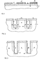
- FIGs 1-6 show a preferred fabrication method for the structure of FIG. 6 with the steps being recited in preferred order and each function accomplished by a preferred specified processing step.
- the N-type substrate 11 may comprise silicon or silicon- on-sapphire. It is covered with a photoresist layer 13 which is masked, exposed to actinic radiation, and the photoresist removed where soluble in the regions 15 and 17 which outlines the portions of the substrate to be slotted or recessed around the boundary of the active region 19 for a single transistor shown as that region covered by the photoresist 13'.
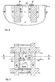
- slots 21 and 23 have been milled into substrate 11 in the regions 17 and 15 while the other regions were protected by the photoresist 13. It will be understood that slots or recesses 21 and 23, as shown in FIG. 2, only bound the active region 19 on two sides, but in reality this boundary recessing or slotting extends completely about the transistor active region 19 as illustrated in FIG. 7 wherein the slot portions 21 and 23 are seen as bounding two sides of region 19 whereas slots 25 and 27 bound the other two regions such that the entire active area 19 is bounded by recesses or slots.
- next step in the preferred process is the deposition of arsenic into slots 21 and 23 to form the N+ doped regions 31 and 33 adjacent to the slots 21 and 23 within substrate 11.
- a silicon oxide is grown over the entire exposed surface of substrate 11 as shown at 16 and 16'.
- the slots 21 and 23 are milled deeper as shown by the extensions 21' and 23' which penetrate substrate 11 deeper than the N+ doped regions 31 and 33.
- the silicon dioxide lining slots 21 and 23, as deepened, is removed following conventional practices to prepare for the boron diffusion step best depicted in FIG. 4.
- the P-type eregions are indicated at 35, 35', 35" and 35'".
- the N-type region of substrate 11 is now roughly defined by the line 37. It will be seen that the P region is beneath the slot 21 extension 21' and the slot extension 23 extension 23', and also occupies the region between the N+ active portions 31 and 33.
- slots 21 and 23 are effected, again preferably by ion milling, to extend them to their bottoms 21" and 23" which now penetrates the N region beneath curve 37.
- the substrate 11 is then oxidized sufficiently to fill the slots 21 and 23 completely with silicon oxide and to cover the substrate 11 with a surface layer 51 of silicon oxide.
- the silicon oxide of the recesses or slots completely electrically isolates the N+P N+ action region of the transistor device being formed in the active region within this isolation boundary.
- the oxide has been stripped completely off the top, shown as the oxide.51, as by etching, to allow for the boron B+ implant indicated by the P+ designation.
- One way of achieving this type doping is to use low energy boron diffusion for the P regions and high energy boron diffusion for the P+ regions.
- FIG. 6 a layer of metallization has been applied to the upper surface of the substrate 11, and it has been covered by photoresist and patterned, removed where soluble and the metallization etched away to leave the particular metal conductors 55 and 57 shown in contact with the N+ region 31 and the N+ region 33.
- the base lead 59 has been formed from the metallization and patterning steps, as shown in FIG. 6 such that electrode connections are made to emitter region 31, collector region 33 and base region 59.
- the sectional view for FIG. 6 is taken along the plane 55.
- the transistor of FIG. 7 is sized 4d x 5d to occupy an area of 20d squared, wherein d is a sdimension of 0.4 to 1 micrometer. It may be seen that the vertical dimension comprises the first d for the base region 59, the second d for the spacing between the base region and the emitter region 31, the third d for the width of the emitter region 31 and d + d for the spacing between electrode 55 and the extremes of the N+ region-31 with the fifth d encompassing one recess 25.
- the dimension in the orthogonal direction util_izes the first d for the width of the recess 21, the second d for the spacing to the electrode 59, the third d for the width of the base electrode 59 and the fourth d measures to recess 23.
- these bipolar transistors have extremely small areas and the parasitic capacitance and resistance is also greatly reduced.
- the total size of the transistor is not much greater than the active area of the transistor.
- the base emitter junction capacitance and the collector base capacitance are made very small.
- the base spreading resistance is small. Since the base width can be made small, i.e. approaching approximately 0.1 micrometers, a high gain and low transit time can be achieved. Also, a symmetrical transistor with a very low collector to emitter saturation voltage is available. Further, the collector resistance is also very small.
Landscapes
- Bipolar Transistors (AREA)
- Element Separation (AREA)
Applications Claiming Priority (2)
| Application Number | Priority Date | Filing Date | Title |
|---|---|---|---|
| US22039980A | 1980-12-29 | 1980-12-29 | |
| US220399 | 1980-12-29 |
Publications (2)
| Publication Number | Publication Date |
|---|---|
| EP0055412A2 true EP0055412A2 (de) | 1982-07-07 |
| EP0055412A3 EP0055412A3 (de) | 1982-08-25 |
Family
ID=22823395
Family Applications (1)
| Application Number | Title | Priority Date | Filing Date |
|---|---|---|---|
| EP81110370A Withdrawn EP0055412A3 (de) | 1980-12-29 | 1981-12-11 | NPN-Lateraltransistor und Verfahren zur Herstellung |
Country Status (2)
| Country | Link |
|---|---|
| EP (1) | EP0055412A3 (de) |
| JP (1) | JPS57134968A (de) |
Families Citing this family (2)
| Publication number | Priority date | Publication date | Assignee | Title |
|---|---|---|---|---|
| US4466180A (en) * | 1981-06-25 | 1984-08-21 | Rockwell International Corporation | Method of manufacturing punch through voltage regulator diodes utilizing shaping and selective doping |
| EP0068072A2 (de) * | 1981-07-01 | 1983-01-05 | Rockwell International Corporation | Lateraler PNP Transistor und Herstellungsverfahren |
Family Cites Families (2)
| Publication number | Priority date | Publication date | Assignee | Title |
|---|---|---|---|---|
| JPS51145276A (en) * | 1975-06-10 | 1976-12-14 | Mitsubishi Electric Corp | Semiconductor device |
| US4140558A (en) * | 1978-03-02 | 1979-02-20 | Bell Telephone Laboratories, Incorporated | Isolation of integrated circuits utilizing selective etching and diffusion |
-
1981
- 1981-12-11 EP EP81110370A patent/EP0055412A3/de not_active Withdrawn
- 1981-12-24 JP JP56216178A patent/JPS57134968A/ja active Pending
Also Published As
| Publication number | Publication date |
|---|---|
| EP0055412A3 (de) | 1982-08-25 |
| JPS57134968A (en) | 1982-08-20 |
Similar Documents
| Publication | Publication Date | Title |
|---|---|---|
| US4419150A (en) | Method of forming lateral bipolar transistors | |
| US4466178A (en) | Method of making extremely small area PNP lateral transistor by angled implant of deep trenches followed by refilling the same with dielectrics | |
| US5372960A (en) | Method of fabricating an insulated gate semiconductor device | |
| US5027184A (en) | NPN type lateral transistor with minimal substrate operation interference | |
| EP0083816B1 (de) | Halbleiteranordnung mit einem Verbindungsmuster | |
| US4466180A (en) | Method of manufacturing punch through voltage regulator diodes utilizing shaping and selective doping | |
| JPS6080276A (ja) | 半導体素子の形成方法 | |
| US4415371A (en) | Method of making sub-micron dimensioned NPN lateral transistor | |
| JPS62108538A (ja) | 半導体集積回路構造体 | |
| JPS6228577B2 (de) | ||
| US4816880A (en) | Junction field effect transistor | |
| JPH04239760A (ja) | 半導体装置の製造法 | |
| GB1577405A (en) | High-frequency transistors | |
| US4485551A (en) | NPN Type lateral transistor separated from substrate by O.D.E. for minimal interference therefrom and method for producing same | |
| US4584762A (en) | Lateral transistor separated from substrate by intersecting slots filled with substrate oxide for minimal interference therefrom and method for producing same | |
| EP0055412A2 (de) | NPN-Lateraltransistor und Verfahren zur Herstellung | |
| US5574306A (en) | Lateral bipolar transistor and FET | |
| EP0068072A2 (de) | Lateraler PNP Transistor und Herstellungsverfahren | |
| US4435899A (en) | Method of producing lateral transistor separated from substrate by intersecting slots filled with substrate oxide | |
| US5031014A (en) | Lateral transistor separated from substrate by intersecting slots filled with substrate oxide for minimal interference therefrom | |
| EP0068073A2 (de) | Lateraler PNP Transistor mit minimaler Beeinflussung der Arbeitsweise durch das Substrat und Verfahren zu seiner Herstellung | |
| US5043787A (en) | Extremely small area npn lateral transistor | |
| JPH0620069B2 (ja) | エミツタ直列抵抗を有するバイポーラトランジスタの製造方法 | |
| US5025302A (en) | PNP type lateral transistor with minimal substrate operation interference | |
| EP0068070A1 (de) | Komplementare NPN- und PNP-Lateraltransistoren, die zur minimalen Beeinflussung durch mit Substratoxyd gefüllte Rillen vom Substrat getrennt sind, und Verfahren zu ihrer Herstellung |
Legal Events
| Date | Code | Title | Description |
|---|---|---|---|
| PUAI | Public reference made under article 153(3) epc to a published international application that has entered the european phase |
Free format text: ORIGINAL CODE: 0009012 |
|
| PUAL | Search report despatched |
Free format text: ORIGINAL CODE: 0009013 |
|
| AK | Designated contracting states |
Designated state(s): DE FR GB |
|
| AK | Designated contracting states |
Designated state(s): DE FR GB |
|
| 17P | Request for examination filed |
Effective date: 19830225 |
|
| STAA | Information on the status of an ep patent application or granted ep patent |
Free format text: STATUS: THE APPLICATION IS DEEMED TO BE WITHDRAWN |
|
| 18D | Application deemed to be withdrawn |
Effective date: 19840809 |
|
| RIN1 | Information on inventor provided before grant (corrected) |
Inventor name: SOCLOF, SIDNEY ISAAC |