EP0055014A2 - Taktgenerator mit variabler Pulsbreitensteuerung - Google Patents
Taktgenerator mit variabler Pulsbreitensteuerung Download PDFInfo
- Publication number
- EP0055014A2 EP0055014A2 EP81304885A EP81304885A EP0055014A2 EP 0055014 A2 EP0055014 A2 EP 0055014A2 EP 81304885 A EP81304885 A EP 81304885A EP 81304885 A EP81304885 A EP 81304885A EP 0055014 A2 EP0055014 A2 EP 0055014A2
- Authority
- EP
- European Patent Office
- Prior art keywords
- clock
- output means
- external
- pulses
- gate
- Prior art date
- Legal status (The legal status is an assumption and is not a legal conclusion. Google has not performed a legal analysis and makes no representation as to the accuracy of the status listed.)
- Granted
Links
Images


Classifications
-
- H—ELECTRICITY
- H03—ELECTRONIC CIRCUITRY
- H03K—PULSE TECHNIQUE
- H03K5/00—Manipulating of pulses not covered by one of the other main groups of this subclass
- H03K5/01—Shaping pulses
- H03K5/02—Shaping pulses by amplifying
- H03K5/023—Shaping pulses by amplifying using field effect transistors
-
- G—PHYSICS
- G09—EDUCATION; CRYPTOGRAPHY; DISPLAY; ADVERTISING; SEALS
- G09G—ARRANGEMENTS OR CIRCUITS FOR CONTROL OF INDICATING DEVICES USING STATIC MEANS TO PRESENT VARIABLE INFORMATION
- G09G5/00—Control arrangements or circuits for visual indicators common to cathode-ray tube indicators and other visual indicators
- G09G5/18—Timing circuits for raster scan displays
-
- H—ELECTRICITY
- H03—ELECTRONIC CIRCUITRY
- H03K—PULSE TECHNIQUE
- H03K5/00—Manipulating of pulses not covered by one of the other main groups of this subclass
- H03K5/01—Shaping pulses
- H03K5/04—Shaping pulses by increasing duration; by decreasing duration
- H03K5/05—Shaping pulses by increasing duration; by decreasing duration by the use of clock signals or other time reference signals
Definitions
- This invention relates to a variable pulsewidth gated clock generator and more particularly to such a generator for the provision of timing signals in a digital display unit.
- Such digital display units may be custom made or may be formed of conventional commercial television sets. In either case, the information displayed is usually of the nature of characters formed of dot matrix where the display unit employs a raster scan mode. Each horizontal line is divided into a number of discrete points or areas called picture elements (PELS) or pixels. A fraction of such picture elements per line is not employed for information display but is that portion of the scan time required for horizontal retrace and synchronization of the horizontal oscillator.
- PELS picture elements
- the dot matrix characters are formed by character generation circuits that control the modulation of the electron beam (in the case of CRT displays), individual circuits of which are selected by character codes that are stored in the memory.
- This code store can be a shift register with exactly the same number of cells as there are character positions on the display screen, or it may be a random access memory.
- 25 to 30 complete scans of all the lines making up the display are made per second.
- each portion of a character being displayed is on display 25 to 30 times a second for a brief period and this can cause an apparent flickering.
- the flickering problem is normally solved by refreshing or redrawing all the lines in the display in two consecutive interlaced scans.
- a "half-scan" is redrawn or refreshed in half the time. Because of the 2:1 interlace between the two half- scans, if a horizontal line is drawn in one half-scan and is adjacent to a line drawn in the next half-scan, the two form a line on the display screen with reduced flicker because, in essence, it is written twice as often.
- a 6 X 8 dot matrix character can be displayed on a 12 X 16 dot matrix, by displaying each dot in the 6 X 8 matrix four times. This reduces flicker considerably, as the character now seems to be written 50 to 60 times a second, instead of 25 to 30 times.
- the respective registers and gates in the video output circuit and the buffer circuit be driven by a very fast clock, of the order of magnitude of 12 megahertz or higher. Since the respective video output circuits and buffer circuits are implemented in integrated circuit silicon chips, the respective circuits are driven by an external clock of appropriate frequency. However, many of the clock signals required to drive the respective circuits may not be of the-same time duration as are the high speed external clock signals. Therefore, it is desirable to be able to provide a clock generator that is driven by an external clock but can nevertheless vary the output cldck signal in a manner determined by logic internal to the integrated circuit chip. It is, therefore, an object of the present invention to provide an improved gated clock generator for employment with the video output circuit of a digital display.
- the present invention is directed toward a gated clock generator for a video output circuit which is driven by a two-phase clock.
- the gated circuit includes a latch which is set by the first phase of the two-phase clock as well as the logic to turn on a bootstrapped output driver to generate a large output signal during the second phase of the two-phase clock.
- the latch is adapted to remain set as long as there is an input signal so that the generated output signal will be of the same duration of time as the input signal irrespective of the two phases of the two-phase clock.
- FIG. 1 A digital display system of the type employing the present invention is illustrated in Figure 1. As shown therein, stored information structures are fetched from information storage 10 by character display processor 11 which controls the communication between storage 10 and the video output circuit employing the present invention. Character codes from the display processor 11 are received by line buffer 12 for sequential presentation to the video output circuit 13. As indicated in Figure 1, video output - circuit 13 includes both the character generation circuitry and the video synthesization circuitry. The system of the present invention is adapted to provide video signals to a commercial video monitor 14.
- the picture on the display monitor 14 is refreshed or redrawn a number of times per second, 25 to 30 times per second in the system in which the present system resides. For this reason, there has to be a storage for the information to be displayed during each scan of the display.
- Line buffer 12 of Figure 1 provides this capability.
- the character generator of the present invention generates the signals for each character dot-matrix pattern.
- Figure 2A illustrates as an example, the dot-matrix pattern for the letter "A".
- the dot matrix in this example, is an area of 16 rows of 8 picture elements each.
- the character "A" is defined by those areas marked by "X's" which represent the picture element on the display screen that will be activated during the character generation or appear as light dots on the display screen with the blank areas in Figure 2A representing dark dots or inactivated areas.
- the character created on the display screen is represented by the dark and light areas according to the character pattern.
- the video output circuit employing the present invention can generate four character sizes depending upon two status bits, high and wide, of the status code which precedes the character code and specifies the mode in which the character is to be displayed. If both of these bits are 0, a normal-sized character with 8 columns and 16 rows is generated.
- a row address is also provided to the video output circuitry to specify the start of each horizontal line.
- the row address is used with the status bits for highlights: superscript, subscript, and high, to determine which horizontal row of the character font is output for the present scan line. Other highlights can be specified by appropriate bits in the status code.
- the Bright and Reverse bits control the intensity levels assigned to the foreground and the background shades. These four combinations include various combinations of gray, black, and white for both the foreground and the background. -When the Underline status bit is set, the two scan lines below the character are set to the foreground shade for that character.
- the Blank or Invisible bit causes the entire character, including the Underline, to be displayed as a background shade.
- Figure 3 illustrates the signals that the line buffer circuit and the video output circuit employ to communicate with the rest of the system and with each other.
- the rate at which the 17 input signals, DATA 1-15, and BLANKOUT are shifted into the circuit is dependent upon both frequency of the external clock and the readiness of the line buffer circuit to accept new data.
- the readiness is characterized by the state of the REQUEST (REQ) signal.
- REQ REQUEST
- On the output side of the circuit information is transferred to the video output circuit in 10-bit quantities at a rate exactly equal to the pixel .rate divided by four. Synchronization with the video monitor is made possible through the horizontal sync signal HPIX whose main purpose is to bracket the activity part of the video scan line.
- the RESET line shown in Figure 3 is common to the whole video system of synchronization during power-up.
- two other output leads are assigned to the END FIELD and END OF VERTICAL RETRACE signals.
- the storage or line buffers are implemented by two 80 X 20 sequentially accessed memories. Each 20-bit word fully describes one of the 80 displayable characters. Eight bits of the character code address the character font of the video output circuit to select one of 256 characters, along with two "Font Select" bits to allow selection of a particular video output circuit. Ten bits of the status (or "highlight”) information contribute to the general appearance of the character such as its size, brightness, position relative to the character line, background shade, and so forth.
- the same sequence of 80 pairs of data is sent to the video output circuit for each scan line. These 160 transfers take place within 160 clock/four periods, and are preceded by a 10-bit row address which specifies which row.of the character dot-matrix is to be displayed on the present scan line.
- the data must be read from the line buffer a number of times equal to the scan line pairs for that particular character line. At the end of every scan line, the register holding the row address is incremented and points to the next scan to be displayed.
- Communication on the input side of the line buffer circuit is attained by two signals, REQUEST and TAKE IT.
- the line buffer circuit When the line buffer circuit is empty and can accept a new character, it raises its REQUEST signal and keeps it high until TAKE IT signal goes high, at which- time a new set of data on the data input lines is strobed into the line buffer. At this time, the line buffer circuit is able to process that particular character immediately and keeps its REQUEST signal high for another clock period, indicating it can process a second character right away. However, no more than two characters can be processed consecutively. At this time, the line buffer circuit is unable to process another character. This is characterized by the REQUEST signal going low after the second set of data has been strobed in.
- the output signals of the system must be supplied constantly at the video frequency.
- the video output circuit of Figure 3 receives data signals that are either a row address, a status code, or a character code which are employed to specify the character to be displayed, the scan line at which the display is to start and various highlights of the display of the character.
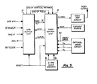
- the synchronization circuitry of Figure 3 is illustrated in more detail in Figure 4 and includes the vertical sync generator 16 and horizontal timing circuitry 19.
- Vertical sync generator 16 examines a row address register. If the two high order bits of the register have been set, vertical sync generator 16 generates the vertical retrace sequence for the timing patterns provided by horizontal timing circuitry 19.
- horizontal timing circuitry 19 generates horizontal sync signals for the video output circuit and the respective HPIX and clock/four timing signals for the line buffer circuitry. Horizontal timing circuitry 19 also generates additional signals which are employed by various portions of the video output circuit.
- the present invention is directed toward a clock generator for the generation of clock signals in a video output circuit or in other integrated circuits which are to operate at clock rates significantly faster than conventional integrated circuits (or require very minimal clock skew) and of the order of 12.3 megahertz and greater.
- each integrated circuit is supplied with external clocks and the purpose of the clock generator of the present invention is to translate the high ramp rate of the external clock to the various gates in the integrated circuit and yet to be able to vary the pulsewidth of those internal clock signals as determined by conditions (logic) within the circuit.
- an integrated circuit 20 is illustrated in Figure 5 in which are implemented one or more clock generators 21A,...,C to drive various gates within the circuit.
- the respective clock generators are supplied with logic signals L1,...L3 which determine the time duration of the respective output clock pulses.
- the respective clock generators are supplied by a two-phase' clock by way of input terminals 22A and B.
- the external two-phase clock is made up of two phases, ⁇ 1 and ⁇ 2 , where ⁇ 1 serves to set the various logic circuitry and ⁇ 2 is employed to provide the output signal therefrom.
- ⁇ 1 serves to set the various logic circuitry
- ⁇ 2 is employed to provide the output signal therefrom.
- a clock generator of the present invention is illustrated in Figure 6.
- a logic input signal IN during clock time ⁇ 1 places FET gates 24 and 27 in a conducting condition where gate 24 along with depletion FET gate 25 form a typical inverter circuit. This causes node 1 to rise in voltage, thus conditioning gate 29.
- gate 29 With gate 29 in a conducting condition, the capacitance of gate 30 is charged during clock time ⁇ 2 .
- Gates 29 and 30 form a double bootstrap configuration where gate 30 has a larger area configuration and a larger capacitance and it is gate 30 which drives the output signal during time ⁇ 2 . Because of the smaller capacitance of gate 29, it is more quickly discharged when clock ⁇ 2 goes low and, therefore, gate 30 is turned off before the output can discharge.
- the output signal is not allowed to go low until the logic IN signal to gate 23 goes low due to the dynamic latch action of gates 24, 25, 26 and 27.
- Gate 33 serves as a resistor to prevent leakage during the time when phase 0 2 is low. This output signal will remain high until such time as the.logic IN signal to.gate 23 is no longer present during a subsequent phase ⁇ 1 .
- Gates 31 and 32 are pull-down devices which are turned'on during phase 0 2 when the logic IN is low.
- gates 24 and 33 are depletion transistors while gates 27, 29, and 30 are control enhancement transistors. That is to say, they are formed by an implantation technique so as to have a lower threshold value and, therefore, a faster turn-on characteristic. While the preferred embodiment of the present invention employs such controlled enhancement devices, the circuit of the present invention can be constructed out of only standard enhancement and depletion devices.
- Figure 7 is a set of waveforms which more clearly illustrate the relation between the output signal and the two external clock signals as determined by the logic IN signal in Figure 6. As illustrated therein, an output signal is generated with the beginning of the ⁇ 2 clock signal, but only when the circuit has received a logic IN signal during or prior to the ⁇ 1 clock signal. The output signal remains high until the IN signal goes low.
- FIG 8 is a more detailed illustration of the waveforms.
- the circuit is not set by clock ⁇ 1 until such time as there is a logic IN signal.
- node2 (see Figure 6) drops to a low value while node1 rises to a high value, thus setting the circuit for output during the next clock ⁇ 2 .
- the above-described gated clock circuit provides a number of advantages over prior art gated clock circuits.
- In the first place there is very little delay between the clock input and the clock output due to the logic circuitry of the clock generator. Such delay is minimized due to the fact that the output drive transistor 30 is a very low impedance transistor and its pulsewidth can be completely variable by the circuit of the present invention.
- output transistor 30, because of its . characteristics is able to drive a large output capacitance and a large load in a very short amount of time.
- the clock generator of the present invention is capable of providing an output signal with a rise time of less than 10 nanoseconds. This is accomplished by the double bootstrap arrangements of gates 30 and 29 where gate 29 will have a very low capacitance relative to the capacitance of the output circuitry.
- a variable pulsewidth gated clock generator has been described above which is able to provide output clock signals with the same rise rate as an external driving clock with the output signal being varied in duration according to logic conditions within the integrated circuit.
- the circuit of the present invention as disclosed includes a latch which is set by the first phase of a two-phase clock to set the internal logic of the circuit to generate a large output signal during the second phase of the two-phase clock.
Landscapes
- Physics & Mathematics (AREA)
- Engineering & Computer Science (AREA)
- Nonlinear Science (AREA)
- Multimedia (AREA)
- Computer Hardware Design (AREA)
- General Physics & Mathematics (AREA)
- Theoretical Computer Science (AREA)
- Controls And Circuits For Display Device (AREA)
Applications Claiming Priority (2)
| Application Number | Priority Date | Filing Date | Title |
|---|---|---|---|
| US06/218,479 US4441037A (en) | 1980-12-22 | 1980-12-22 | Internally gated variable pulsewidth clock generator |
| US218479 | 1994-03-25 |
Publications (3)
| Publication Number | Publication Date |
|---|---|
| EP0055014A2 true EP0055014A2 (de) | 1982-06-30 |
| EP0055014A3 EP0055014A3 (en) | 1983-01-26 |
| EP0055014B1 EP0055014B1 (de) | 1985-08-28 |
Family
ID=22815285
Family Applications (1)
| Application Number | Title | Priority Date | Filing Date |
|---|---|---|---|
| EP81304885A Expired EP0055014B1 (de) | 1980-12-22 | 1981-10-20 | Taktgenerator mit variabler Pulsbreitensteuerung |
Country Status (4)
| Country | Link |
|---|---|
| US (1) | US4441037A (de) |
| EP (1) | EP0055014B1 (de) |
| CA (1) | CA1190608A (de) |
| DE (1) | DE3172052D1 (de) |
Families Citing this family (1)
| Publication number | Priority date | Publication date | Assignee | Title |
|---|---|---|---|---|
| GB8303587D0 (en) * | 1983-02-09 | 1983-03-16 | Chapman Cash Processing Ltd | Coin discriminating apparatus |
Family Cites Families (9)
| Publication number | Priority date | Publication date | Assignee | Title |
|---|---|---|---|---|
| US3599018A (en) * | 1968-01-25 | 1971-08-10 | Sharp Kk | Fet flip-flop circuit with diode feedback path |
| US3585408A (en) * | 1969-07-17 | 1971-06-15 | Shell Oil Co | Mosfet circuit for extending the time duration of a clock pulse |
| JPS5937614B2 (ja) * | 1972-07-21 | 1984-09-11 | 株式会社日立製作所 | 絶縁ゲ−ト型トランジスタを用いたブ−トスラツプ回路 |
| US3946322A (en) * | 1974-06-17 | 1976-03-23 | The United States Of America As Represented By The Secretary Of The Navy | Pulse duty cycle transition moderating device |
| DE2608265C2 (de) * | 1976-02-28 | 1978-04-27 | Deutsche Itt Industries Gmbh, 7800 Freiburg | Mehrphasen-MOS-Schaltung zur Impulsdaueränderung |
| US4035663A (en) * | 1976-09-01 | 1977-07-12 | Rockwell International Corporation | Two phase clock synchronizing method and apparatus |
| DE2657281C3 (de) * | 1976-12-17 | 1980-09-04 | Deutsche Itt Industries Gmbh, 7800 Freiburg | MIS-Inverterschaltung |
| JPS5590383A (en) * | 1978-12-27 | 1980-07-08 | Canon Inc | Thermal printer |
| US4272690A (en) * | 1979-08-16 | 1981-06-09 | The United States Of America As Represented By The Secretary Of The Army | Clock controlled pulse width modulator |
-
1980
- 1980-12-22 US US06/218,479 patent/US4441037A/en not_active Expired - Fee Related
-
1981
- 1981-10-20 EP EP81304885A patent/EP0055014B1/de not_active Expired
- 1981-10-20 DE DE8181304885T patent/DE3172052D1/de not_active Expired
- 1981-12-17 CA CA000392503A patent/CA1190608A/en not_active Expired
Also Published As
| Publication number | Publication date |
|---|---|
| DE3172052D1 (en) | 1985-10-03 |
| EP0055014A3 (en) | 1983-01-26 |
| CA1190608A (en) | 1985-07-16 |
| EP0055014B1 (de) | 1985-08-28 |
| US4441037A (en) | 1984-04-03 |
Similar Documents
| Publication | Publication Date | Title |
|---|---|---|
| KR100426913B1 (ko) | 표시 장치, 화상 제어 반도체 장치, 및 표시 장치의 구동방법 | |
| US4511965A (en) | Video ram accessing system | |
| US4486856A (en) | Cache memory and control circuit | |
| US20040183766A1 (en) | Driver circuit for display device | |
| US4328557A (en) | Processor circuit for video data terminal | |
| US4485378A (en) | Display control apparatus | |
| US4574277A (en) | Selective page disable for a video display | |
| JPH0677183B2 (ja) | ビデオ・モ−ドで動作するプラズマ表示装置 | |
| US20250104660A1 (en) | Driving method for display panel, driving apparatus for display panel, and display apparatus | |
| US4345244A (en) | Video output circuit for high resolution character generator in a digital display unit | |
| JPH0760305B2 (ja) | ビデオ表示制御回路 | |
| US4409591A (en) | Variable size character generator | |
| US4683469A (en) | Display terminal having multiple character display formats | |
| KR860001450B1 (ko) | 그래픽 디스플레이 시스템 | |
| EP0215984B1 (de) | Graphik-Anzeigegerät mit kombiniertem Bitpuffer und Zeichengraphikspeicherung | |
| US4956708A (en) | Frame memory control system | |
| US4390780A (en) | LSI Timing circuit for a digital display employing a modulo eight counter | |
| US4365242A (en) | Driving technique for matrix liquid crystal display panel for displaying characters and a cursor | |
| US4613856A (en) | Character and video mode control circuit | |
| JPH0141993B2 (de) | ||
| US4441037A (en) | Internally gated variable pulsewidth clock generator | |
| JPS6353558B2 (de) | ||
| US4581611A (en) | Character display system | |
| US5736972A (en) | Liquid crystal display apparatus capable of displaying a complete picture in response to an insufficient video signal | |
| US4281393A (en) | Programmable computer terminal system |
Legal Events
| Date | Code | Title | Description |
|---|---|---|---|
| PUAI | Public reference made under article 153(3) epc to a published international application that has entered the european phase |
Free format text: ORIGINAL CODE: 0009012 |
|
| 17P | Request for examination filed |
Effective date: 19811029 |
|
| AK | Designated contracting states |
Designated state(s): BE DE FR GB IT NL |
|
| PUAL | Search report despatched |
Free format text: ORIGINAL CODE: 0009013 |
|
| AK | Designated contracting states |
Designated state(s): BE DE FR GB IT NL |
|
| ITF | It: translation for a ep patent filed | ||
| GRAA | (expected) grant |
Free format text: ORIGINAL CODE: 0009210 |
|
| AK | Designated contracting states |
Designated state(s): BE DE FR GB IT NL |
|
| REF | Corresponds to: |
Ref document number: 3172052 Country of ref document: DE Date of ref document: 19851003 |
|
| ET | Fr: translation filed | ||
| ITPR | It: changes in ownership of a european patent |
Owner name: FUSIONI;BURROUGHS DELAWARE INCORPORATED ( DETROIT |
|
| PLBE | No opposition filed within time limit |
Free format text: ORIGINAL CODE: 0009261 |
|
| STAA | Information on the status of an ep patent application or granted ep patent |
Free format text: STATUS: NO OPPOSITION FILED WITHIN TIME LIMIT |
|
| 26N | No opposition filed | ||
| PGFP | Annual fee paid to national office [announced via postgrant information from national office to epo] |
Ref country code: FR Payment date: 19921009 Year of fee payment: 12 |
|
| PGFP | Annual fee paid to national office [announced via postgrant information from national office to epo] |
Ref country code: DE Payment date: 19921026 Year of fee payment: 12 |
|
| PGFP | Annual fee paid to national office [announced via postgrant information from national office to epo] |
Ref country code: NL Payment date: 19921031 Year of fee payment: 12 |
|
| PGFP | Annual fee paid to national office [announced via postgrant information from national office to epo] |
Ref country code: BE Payment date: 19921116 Year of fee payment: 12 |
|
| PG25 | Lapsed in a contracting state [announced via postgrant information from national office to epo] |
Ref country code: BE Effective date: 19931031 |
|
| BERE | Be: lapsed |
Owner name: BURROUGHS CORP. (A MICHIGAN CORP.) Effective date: 19931031 |
|
| PG25 | Lapsed in a contracting state [announced via postgrant information from national office to epo] |
Ref country code: NL Effective date: 19940501 |
|
| NLV4 | Nl: lapsed or anulled due to non-payment of the annual fee | ||
| PG25 | Lapsed in a contracting state [announced via postgrant information from national office to epo] |
Ref country code: FR Effective date: 19940630 |
|
| PG25 | Lapsed in a contracting state [announced via postgrant information from national office to epo] |
Ref country code: DE Effective date: 19940701 |
|
| REG | Reference to a national code |
Ref country code: FR Ref legal event code: ST |
|
| PGFP | Annual fee paid to national office [announced via postgrant information from national office to epo] |
Ref country code: GB Payment date: 19940927 Year of fee payment: 14 |
|
| PG25 | Lapsed in a contracting state [announced via postgrant information from national office to epo] |
Ref country code: GB Effective date: 19951020 |
|
| GBPC | Gb: european patent ceased through non-payment of renewal fee |
Effective date: 19951020 |