EP0052918A2 - Plasma display pilot cell driver device - Google Patents
Plasma display pilot cell driver device Download PDFInfo
- Publication number
- EP0052918A2 EP0052918A2 EP81303935A EP81303935A EP0052918A2 EP 0052918 A2 EP0052918 A2 EP 0052918A2 EP 81303935 A EP81303935 A EP 81303935A EP 81303935 A EP81303935 A EP 81303935A EP 0052918 A2 EP0052918 A2 EP 0052918A2
- Authority
- EP
- European Patent Office
- Prior art keywords
- pilot cell
- pull
- voltage
- pilot
- driver device
- Prior art date
- Legal status (The legal status is an assumption and is not a legal conclusion. Google has not performed a legal analysis and makes no representation as to the accuracy of the status listed.)
- Granted
Links
Images


Classifications
-
- G—PHYSICS
- G09—EDUCATION; CRYPTOGRAPHY; DISPLAY; ADVERTISING; SEALS
- G09G—ARRANGEMENTS OR CIRCUITS FOR CONTROL OF INDICATING DEVICES USING STATIC MEANS TO PRESENT VARIABLE INFORMATION
- G09G3/00—Control arrangements or circuits, of interest only in connection with visual indicators other than cathode-ray tubes
- G09G3/20—Control arrangements or circuits, of interest only in connection with visual indicators other than cathode-ray tubes for presentation of an assembly of a number of characters, e.g. a page, by composing the assembly by combination of individual elements arranged in a matrix no fixed position being assigned to or needed to be assigned to the individual characters or partial characters
- G09G3/22—Control arrangements or circuits, of interest only in connection with visual indicators other than cathode-ray tubes for presentation of an assembly of a number of characters, e.g. a page, by composing the assembly by combination of individual elements arranged in a matrix no fixed position being assigned to or needed to be assigned to the individual characters or partial characters using controlled light sources
- G09G3/28—Control arrangements or circuits, of interest only in connection with visual indicators other than cathode-ray tubes for presentation of an assembly of a number of characters, e.g. a page, by composing the assembly by combination of individual elements arranged in a matrix no fixed position being assigned to or needed to be assigned to the individual characters or partial characters using controlled light sources using luminous gas-discharge panels, e.g. plasma panels
- G09G3/288—Control arrangements or circuits, of interest only in connection with visual indicators other than cathode-ray tubes for presentation of an assembly of a number of characters, e.g. a page, by composing the assembly by combination of individual elements arranged in a matrix no fixed position being assigned to or needed to be assigned to the individual characters or partial characters using controlled light sources using luminous gas-discharge panels, e.g. plasma panels using AC panels
- G09G3/296—Driving circuits for producing the waveforms applied to the driving electrodes
Definitions
- This invention relates to plasma display pilot cell driver devices.
- the A.C. (alternative current) plasma display capacitive memory panel is well-known in the display technology art.
- Plasma display pilot cell techniques for such panels are also well-known.
- the present invention seeks to provide a plasma display pilot cell driver device haviog three output states, particularly, a high, pull-up state, a low, pull-down state, and a relaxation, floating state which allows the achievement of a pilot cell electrode voltage which is not directly supplied by an external voltage source.
- pilot cells have been fired coincident with the write pulse to achieve photon conditioning and provide for reliable writing of isolated display cells. Pilot cells have been operated in the bistable mode and in some cases have had additional write pulses applied to them to initiate pilot cell discharges and to maintain the lighted condition of pilot cells following a bulk erase operation or other disturbing condition in the operation of the display panel.
- the system described in this application prevents all of these operational features.
- the present invention seeks to provide a simple pull-up/pull-down pilot cell driver device rather than a comparatively complex, multi state pilot cell driver device. Additional pilot cell writing pulse voltages for rewriting of pilot cells may be derived from the opposite axis sustain drive voltage through a feedback or coupling network.
- the operation of the pilot cell driver device is as a result of allowing the output of the pilot cell driver to float during a portion of the pilot cell drive cycle and controlling the feedback of the sustain voltage so that the appropriate rewrite pulse amplitude is achieved.
- U .S. Patent Specification No. 3 786 484 shows border elements, otherwise called pilot cells, operating in a sustain voltage range and capable of being written at a selected time by increasing the direct current supply voltage input to the border sustainer.
- U .S. Patent Specification No. 3 879 634 shows the use of pilot cells in a plasma display panel and describes the use of such cells to maintain photon conditioning of a plasma display panel.
- a plasma display pilot cell driver device associated with at least one axis of a plasma display device characterised by comprising: a pull-up switch connected with a source of voltage; a pull-down switch connected with a source of voltage; means for allowing the output of said pilot cell driver device to float with the voltage applied to pilot cell drive electrodes; and means for supplying opposite axis sustain voltage feedback to said pilot cell drive electrodes.
- Said pull-up and said pull-down switches may be bipolar transistor switches.
- the pilot cell driver device preferably is arranged so that the opposite axis sustain voltage feedback is coupled to said output during a relaxation period following momentary actuation of said pull-up bipolar transistor switch to achieve a floating output voltage condition.
- the pilot cell driver device may include a capacitor to couple the opposite axis sustain voltage feedback to said pilot cell drive electrodes to achieve said floating output voltage condition.
- Said capacitor in operation, may act to create a voltage divider network for said floating output voltage together with the internal capacitance of said plasma display device and the internal capacitance of the pilot cell driver device.
- the pilot cell driver device may be arranged so that the floating output voltage of the pilot cell driver device (V p ) is defined by a relationship to the opposite axis sustain voltage (V ) as follows:
- the pilot cell driver device in a preferred embodiment is arranged so that the following relationship exists: where:
- the pull-down switch may be connected with a ground reference.
- a plasma display pilot cell driver device associated with one axis of a plasma display device characterised by comprising: a pilot cell driver output bus; a bipolar pull-up transistor switch connected from a source of write voltage to said bus; a pilot pull-up trigger means connected to actuate said pull-up transistor switch; a bipolar pull-down transistor switch connected to a reference voltage source; a pilot pull-down trigger means connected to actuate said pull-down transistor switch; diode biasing means connecting said pull-down transistor switch to the base of said transistor pull-up switch and to said bus for shutting off said pull-up switch upon actuation of said pull-down switch; and means for capacitively coupling said output bus to an opposite axis sustain driver so that the voltage on said output bus is a floating voltage during a relaxation period following momentary actuation of said pull-up switch when said pull-down switch is not actuated.
- a capacitive memory plasma display panel 10 shown diagrammatically, is provided with a vertical write/erase selection driver unit 12 to drive a plurality of vertical electrodes or drive lines, shown diagrammatically.
- a horizontal write/erase selection driver unit 14 provides the horizontal voltages to the various horizontal electrodes.
- the plasma display panel also has a plurality of vertially aligned pilot cells driven by at least one pilot cell electrode 16.
- the characteristics of the pilot cell electrode 16 include, particularly, that the pilot cell electrode exhibits a capacitive coupling with all of the other elements of the plasma display panel. This is illustrated by means of a characterising capacitance 18, shown for diagrammatic purposes only, between the pilot cell electrode 16 and a single, illustrative, horizontal electrode 20 in the display panel.
- the capacitance 18 is referred to as the C capacitance in the following discussion of this characteristic of the plasma display panel.
- the horizontal electrodes are driven by horizontal electrode voltages V B .
- the pilot cell electrode 16 is driven by a voltage V p .
- the plasma display panel has a sustain driver voltage which is supplied by a sustain driver unit 22 which drives a sustain bus 24 which is coupled to the horizontal write/erase selection'driver unit 14.
- the sustain driver unit 22 may be simply characterised as consisting of four switches 26, 28, 30, 32 for pulling the sustain bus 24 to the four voltages necessary for appropriately driving a plasma display panel. These four switches are coupled, respectively, to a source of erase voltage V E , sustain voltages V S , write voltages V and a ground reference.
- the erase voltage V E may be 40 volts for example.
- the sustain voltage V may be approximately 190 volts.
- the write voltage V W may be 130 volts, for example.
- a plasma display pilot cell driver device 34 according to the present invention is connected with a pilot cell bus 36 which in turn is connected with the pilot cell electrode 16.
- the sustain bus 24 is coupled by means of a feedback bus 38 to the pilot cell driver device.
- the pilot cell driverdevice 34 consists of a pilot pull-up (PPU) switch 40 connected to a source of pilot writing voltage V w which is 130 volts and is the same as the write voltage supplied to the sustain driver unit 22.
- the pilot pull-up switch 40 is connected to an internal bus 42 which in turn is connected externally to the pilot cell bus 36.
- the pilot cell driver device has a pilot pull-down (PPD) switch 44 connected between the internal bus 42 and a source of pull-down voltage which may typically be a ground reference.
- PPD pilot pull-down
- the pull-down voltage for a pilot cell driverdevice does not have to be a ground reference voltage.
- the internal capacitance of the pilot cell driver device which consists of the aggregate of the internal capacitances of the various transistor switches and other elements of the pilot cell driver device, is represented by a capacitor 46 with a characteristic capacitance C s .
- a coupling capacitor 48 with a capacitance C 1 , is connected between the feedback bus 38 and the internal bus 42.
- a capacitor 50 with a capacitance C 2' is coupled between the internal bus 42 and a ground reference voltage.
- FIG 2 is a diagrammatic illustration of the voltage waveform characteristics of the plasma display panel of Figure 1 in the basic operating modes.
- the voltages shown are by way of example, only, but are typical and appropriate for plasma display panels.
- the time duration of each of these cycles is approximately 20 microseconds.
- the start-up cycle is used when the display panel is first turned on to initiate pilot cell discharges.
- the sustain waveform is applied to all of the panel electrodes until such time as the panel is to be addressed.
- a write cycle is used to selectively apply a pulse to one of the display elements and cause that element to become ignited.
- the erase pulse is used to selectively erase an already discharging display element.
- the bulk erase cycle is applied to nonselectively erase all of the lit display elements of the panel.
- the horizontal electrode voltage V H is generated by the sustain driver unit 22 in combination with the horizontal write/erase selection driver unit 14 and is applied to all horizontal electrodes on the display panel.
- a vertical pilot cell electrode voltage Vp is generated by the pilot cell driver device.
- This waveform is modified, during the floating condition, by the feedback voltages that are coupled both through the capacitance 18 and through the capacitor 48.
- This composite waveform (V ) is applied to one or more pilot cell electrodes although only one is shown.
- the input timing or trigger signals, a pilot pull-up (PPU) signal and a pilot pull-down (PPD) signal are applied, respectively, to the pilot pull-up switch 40 and the pilot pull-down switch 44 of the pilot cell driver device.
- the voltage that is seen by the pilot cell elements within the panel is the algebraic combination of the horizontal voltage V H and the vertical pilot cell electrode voltage V , that is, (V minus V).
- the switch 28 and the switch 32 of the sustain driver unit are used to create a rectangular pulse 60.
- the switches 40, 44 in the pilot cell driver device are turned on and off with trigger or timing pulses 62, 64.
- the output voltage of the pilot cell driver device,V p when combined with the pulse 60 from the sustain driver unit creates a large, rectangular peak-to-peak voltage pulse 66 across the pilot cell elements.
- pilot cell driver device 34 and the sustain driver unit 22 By timing the pilot cell driver device 34 and the sustain driver unit 22 in this way during the start-up cycle, a voltage that is in excess of the normal sustain voltage is applied to the pilot'elements. This voltage makes the pilot cells start more rapidly during the initial start-up of the plasma display panel.
- a complex waveform having several voltage levels is applied by the sustain driver unit during the sustain cycle.
- the four levels of the sustain waveform are created by turning on and off the four switches 26, 28, 30, 32 within the sustain driver unit 22.
- the switch 32 When the switch 32 is turned on, the voltage on the sustain bus 24 goes to zero at level 69 on the waveform of Figure 2.
- the switch 26 is then turned on which will pull the voltage of the sustain bus up to 40 volts at level 70 on the waveform.
- the switch 28 is turned on which brings the pulse voltage up to 190 volts at level 72 on the waveform.
- the voltage is then brought back down to 130 volt level at point 74 on the waveform by turning on the switch 30.
- the internal output bus 42 of the pilot cell driver device is in a floating state and the voltage V on the pilot cell bus 36 is generated by the feedback paths within the circuit.
- These feedback conditions are determined by the capacitance 18 through the plasma display panel and the capacitor 48 added as a capacitor direct feedback path from the sustain bus 24 to the internal bus 42 of the pilot cell driver device.
- the voltage at the output of the pilot cell driver device will make a transition from 130 volts to 65 volts. This transition is determined by a feedback capacitance which is the parallel combination of the capacitance 18 in Figure 1 and the capacitor 48.
- the pilot cell driver device has its internal capacitance, C s , shown in Figure 1 as a phantom capacitor 46 and the capacitor 50. Both of these capacitors represent capacitance relative to ground.
- the voltage at the output of the pilot cell driver device V p , during the floating condition is proportional to the change in voltage that occurs on the sustain bus 24.
- the capacitance C l of the capacitor 48 that controls this feedback is adjusted such that the voltage V will be approximately one-half the change in voltage that is occurring on the sustain bus 24. This is shown in the formula in Figure 3: ⁇ V P , the change in the pilot voltage, equals one-half ⁇ V H , which is the change in the applied voltage on the sustain bus 24.
- C 1 + C P C 2 + C S .
- the change in pilot voltage will produce a pulse shown in Figure 2, at level 76, which in relation to the following sustain pulses, will appear as a writing pulse.
- the output of the pilot cell driver device during the first portion of the sustain cycle therefore goes from 130 to 65 volts at level 78 and then makes a transition when the switch 26 of the sustain driver unit pulls to 40 volts. At this time, the transition seen at the output of the pilot cell driver device goes from 65 to 85 volts, to level 80 in Figure 2. This is a 20 volt transition determined by the ratio of the feedback capacitor.
- the feedback circuit creates a capacitive voltage divider based on internal capacitance (C p and C s ) and the capacitors 48 and 50. This voltage divider determines the change of voltage on the pilot cell bus 36 which is half the change of voltage on the sustain bus 24.
- the triangle symbol shown at level 76 represents the time at which the pilot cell element will fire if it has not been firing in the sustaining mode as represented by the X symbol. Thus, a pilot cell element, if it is off, will fire once at the triangle symbol and then continue to fire in the bistable mode at the X symbol shown at points 94, 96.
- the switch 44 of the pilot cell driver device is turned on by a trigger pulse 83 and brings the output of the pilot driver to zero volts at level 82.
- a pilot pull-up trigger pulse 84 is applied to cause the output of the pilot cell driver device to go to its high state, 130 volts at level 86. This is done at the same time as the switches 26, 28, 30, 32 of the sustain driver unit are switching from level 72 to level 74 as shown.
- the result of this combination is a voltage waveform across the pilot cell elements which is shown as V E - Vp in Figure 2.
- the voltage pulse begins at zero at level 88, and switches to minus 65 volts at level 76.
- the voltage then falls to minus 45 volts at level 89, and next makes a transition to plus 190 volts at level 90.
- the final transition during the sustain cycle brings the voltage applied to the pilot cell elements back to zero at level 92.
- the X symbol at points 94, 96 during the sustain cycle represents the normal, bistable firing times of the pilot cell elements. This means that if the pilot cell elements are lit, they will be firing a sustain cycle at the times represented by the X, at points 94, 96. If the pilot cell elements are not lit, they will be fired by the minus 65 volt pulse, at level 76.
- the waveshape is a repeated waveshape and therefore a pulse will occur once each sustain cycle. If for some reason the pilot cell element is off because of some other voltage disturbance, like a bulk erase operation, the pulse will cause the pilot cell element to fire and the pilot cell element will then continue to be sustained at points 94, 96 in the Figure.
- the output of the sustain driver during the write cycle is very similar to the waveshape that is used during a sustain cycle.
- the main difference in a write cycle is that a half-select write pulse shown at 98 is applied at the time the pulse level drops from 190 volt to the 130 volt. This is a selective pulse which will occur only on the drive lines which will have information written into them in the active part of the plasma display panel.
- a very similar waveform is created at the output of the pilot cell driver device and the resultant operation of the pilot cell elements will be the same as if the panel were in the sustain mode.
- pilot cell elements in a plasma display panel The primary purpose of the pilot cell elements in a plasma display panel is to have them fire at the same time as the selective write pulse is applied to the panel.
- the firing of the pilot cell elements will supply photons to enhance the reliability of the writing operation. This occurs when the pilot cell elements fire at approximately the same time as the beginning of the selective write pulse.
- the pilot discharge indicated by the X symbol at point 110 occurs close in time to the leading edge of-the selective write pulse shown at 98.
- the timing is similar to the sustain cycle and the write cycle except that the pulse time at 112 at the 40 volt level is longer so that there will be sufficient time for the half-select erase pulse (shown by pulse 114) to achieve the proper erase condition in the selected cell. Because this additional time is required during the first part of the erase cycle, it is necessary to alter slightly the operation of the pilot cell driver device. Only one of the input timing or trigger pulses to the pilot cell driver device is used during the erase cycle. This is the pilot pull-down trigger pulse shown at 116. It is not necessary that the pilot pull-up trigger pulse be used during the erase cycle to achieve proper operation of the pilot cell elements.
- the reason for this is that it is not important that the pilot cell elements fire during the time the erase pulse is applied because erasing does not require the same conditioning that the write cycle requires.
- the erase cycle still has the same rewrite pulse occurring at the beginning; namely, a pulse 118. If the pilot cell elements are not lit, this rewrite pulse will cause them to write and they will continue to be sustained at the X symbol locations as shown.
- the operation of the pilot cell driver device during the bulk erase cycle is similar to the operation during the sustain cycle and the write cycle.
- the bulk erase cycle is used to extinguish all of the display elements within the active part of the display panel, but is not intended to extinguish the pilot cell elements.
- the bulk erase cycle is generated by changing the timing of the switches within the sustain driver unit so that a narrow pulse 120 occurs at the beginning of the bulk erase cycle. Except for this timing change, the pilot cell operation during the bulk erase cycle will be identical to the operation during the sustain cycle.
- the rewrite pulse that results from the shortened timing sequence of the sustain output shown at 122, will not be adequate for rewriting the pilot cell elements in case the pilot cell elements have been erased or are out for some other reason, independent of the bulk erase operation. Since the bulk erase is only a single event and is not applied repetitively, the rewrite pulse that is at the beginning of any of the other cycles will serve to rewrite the pilot cell elements and thus restore the operation that is required.
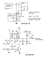
- Figure 4 is a schematic diagram of a pilot cell driver device according to the present invention.
- the primary requirement for the pilot cell driver device is that it be capable of driving its output actively to a high state of approximately 130 volts or to drive the output to a low state which is zero or ground or to allow the output of the driver to be in a floating state so that the voltage condition on the pilot cell bus can be determined by the externally coupled feedback to the voltage supplied by the sustain driver unit on the horizontal axis of the plasma display device.
- a transistor 150 will pull an output line 152 of the pilot cell driver device to the high voltage level V when the transistor is turned on.
- the transistor 150 is turned on as the result of a pilot pull-up pulse being applied to a gate 154. This pulls current through an isolation transformer 168 and thus drives the base of the transistor 150 to turn it on.
- a transistor 156 acts as a pull-down transistor switch. This switch is activated when the pilot pull-down logic signal is applied to a gate 158 which drives the base of the transistor 156.
- the output line 152 will be pulled down through a diode 160 and a diode 162. This diode interconnection allows the base-to- emitter junction of the transistor 150 to be reverse biased during the pull-down time, thus aiding the turn off of the transistor 150 by helping to reduce the storage time of the transistor.
- a capacitor 164 is connected from the output line 152 to the output of the sustain driver bus 24.
- a capacitor 166 is connected from the output line 152 to ground.
- the transformer 168 serves as an isolation transformer between the gate 154 which acts as a ground referenced PPU driver and the transistor 150.
- a resistor 172 in Figure 4 controls the base current drive for the transistor 150.
- a resistor 170 controls the base current drive to transistor 156.
- a diode 174 is connected between the output line 152 and ground.
- the transistors 150 and 156 may be Unitrode model UPT 313 transistors.
- the resistors 170 and 172 may be 180 ohms.
- the capacitor 164 may be 100 picofarads and the capacitor 166 may be 68 picofarads.
Abstract
Description
- This invention relates to plasma display pilot cell driver devices.
- The A.C. (alternative current) plasma display capacitive memory panel is well-known in the display technology art. Plasma display pilot cell techniques for such panels are also well-known. The present invention seeks to provide a plasma display pilot cell driver device haviog three output states, particularly, a high, pull-up state, a low, pull-down state, and a relaxation, floating state which allows the achievement of a pilot cell electrode voltage which is not directly supplied by an external voltage source.
- In the prior art, pilot cells have been fired coincident with the write pulse to achieve photon conditioning and provide for reliable writing of isolated display cells. Pilot cells have been operated in the bistable mode and in some cases have had additional write pulses applied to them to initiate pilot cell discharges and to maintain the lighted condition of pilot cells following a bulk erase operation or other disturbing condition in the operation of the display panel. The system described in this application prevents all of these operational features. The present invention seeks to provide a simple pull-up/pull-down pilot cell driver device rather than a comparatively complex, multi state pilot cell driver device. Additional pilot cell writing pulse voltages for rewriting of pilot cells may be derived from the opposite axis sustain drive voltage through a feedback or coupling network. The operation of the pilot cell driver device is as a result of allowing the output of the pilot cell driver to float during a portion of the pilot cell drive cycle and controlling the feedback of the sustain voltage so that the appropriate rewrite pulse amplitude is achieved.
- In U.S. Patent Specification No. 3 750 159 a bulk erase operation in the display panel automatically erases all pilot cells because the pilot cells are operating in a sustaining mode just as are all of the display panel visible elements. The pilot cell write drivers float on the sustain driver output and each pilot cell write driver is capable of supplying a full write amplitude pulse. Following a bulk erase the pilot write drivers rewrite the pilot elements.
- U.S. Patent Specification No. 3 786 484 shows border elements, otherwise called pilot cells, operating in a sustain voltage range and capable of being written at a selected time by increasing the direct current supply voltage input to the border sustainer.
- U.S. Patent Specification No. 3 879 634 shows the use of pilot cells in a plasma display panel and describes the use of such cells to maintain photon conditioning of a plasma display panel.
- Our earlier U.S. Patent Specifications Nos. 4 077 033 and 4 091 309 contain additional background information relating to the subject of A.C. plasma display technology. The disclosure of these two patent specifications is incorporated herein by reference.
- According to one aspect of the present invention there is provided a plasma display pilot cell driver device associated with at least one axis of a plasma display device characterised by comprising: a pull-up switch connected with a source of voltage; a pull-down switch connected with a source of voltage; means for allowing the output of said pilot cell driver device to float with the voltage applied to pilot cell drive electrodes; and means for supplying opposite axis sustain voltage feedback to said pilot cell drive electrodes.
- Said pull-up and said pull-down switches may be bipolar transistor switches.
- The pilot cell driver device preferably is arranged so that the opposite axis sustain voltage feedback is coupled to said output during a relaxation period following momentary actuation of said pull-up bipolar transistor switch to achieve a floating output voltage condition.
- The pilot cell driver device may include a capacitor to couple the opposite axis sustain voltage feedback to said pilot cell drive electrodes to achieve said floating output voltage condition. Said capacitor, in operation, may act to create a voltage divider network for said floating output voltage together with the internal capacitance of said plasma display device and the internal capacitance of the pilot cell driver device.
- The pilot cell driver device may be arranged so that the floating output voltage of the pilot cell driver device (Vp) is defined by a relationship to the opposite axis sustain voltage (V ) as follows:

- The pilot cell driver device, in a preferred embodiment is arranged so that the following relationship exists:

- C1 is the value of the capacitor providing feedback from the opposite axis sustain voltage,
- Cp is the internal capacitance of the plasma display device, C2 is a capacitor coupling the pilot cell driver system output to a ground reference and
- C is the internal capacitance of the pilot cell driver device.
- The pull-down switch may be connected with a ground reference.
- According to another aspect of the present invention there is provided a plasma display pilot cell driver device associated with one axis of a plasma display device characterised by comprising: a pilot cell driver output bus; a bipolar pull-up transistor switch connected from a source of write voltage to said bus; a pilot pull-up trigger means connected to actuate said pull-up transistor switch; a bipolar pull-down transistor switch connected to a reference voltage source; a pilot pull-down trigger means connected to actuate said pull-down transistor switch; diode biasing means connecting said pull-down transistor switch to the base of said transistor pull-up switch and to said bus for shutting off said pull-up switch upon actuation of said pull-down switch; and means for capacitively coupling said output bus to an opposite axis sustain driver so that the voltage on said output bus is a floating voltage during a relaxation period following momentary actuation of said pull-up switch when said pull-down switch is not actuated.
- The invention is illustrated, merely by way of example, in the accompanying drawings, in which:
- Figure 1 is a diagrammatic illustration of a plasma display panel, a horizontal sustain driver coupled to the plasma display panel and a plasma display pilot cell driver device according to the present invention;
- Figure 2 is an illustrative diagram of horizontal electrode voltages, pilot cell electrode voltages and voltages actually applied to pilot cell elements for various operations of the plasma display panel;
- Figure 3 is a diagram showing effective capacitances which provide a feedback voltage from a sustain driver bus to a pilot cell electrode; and
- Figure 4 illustrates a pilot cell driver device according to the present invention.
- Referring now to Figure 1, a capacitive memory
plasma display panel 10, shown diagrammatically, is provided with a vertical write/erase selection driver unit 12 to drive a plurality of vertical electrodes or drive lines, shown diagrammatically. A horizontal write/erase selection driver unit 14 provides the horizontal voltages to the various horizontal electrodes. The plasma display panel also has a plurality of vertially aligned pilot cells driven by at least onepilot cell electrode 16. The characteristics of thepilot cell electrode 16 include, particularly, that the pilot cell electrode exhibits a capacitive coupling with all of the other elements of the plasma display panel. This is illustrated by means of a characterisingcapacitance 18, shown for diagrammatic purposes only, between thepilot cell electrode 16 and a single, illustrative,horizontal electrode 20 in the display panel. Thecapacitance 18 is referred to as the C capacitance in the following discussion of this characteristic of the plasma display panel. - The horizontal electrodes are driven by horizontal electrode voltages VB. The
pilot cell electrode 16 is driven by a voltage Vp. The plasma display panel has a sustain driver voltage which is supplied by asustain driver unit 22 which drives asustain bus 24 which is coupled to the horizontal write/erase selection'driver unit 14. - The
sustain driver unit 22 may be simply characterised as consisting of fourswitches sustain bus 24 to the four voltages necessary for appropriately driving a plasma display panel. These four switches are coupled, respectively, to a source of erase voltage VE, sustain voltages VS, write voltages V and a ground reference. The erase voltage VE may be 40 volts for example. The sustain voltage V may be approximately 190 volts. The write voltage VW may be 130 volts, for example. A plasma display pilotcell driver device 34 according to the present invention is connected with apilot cell bus 36 which in turn is connected with thepilot cell electrode 16. In addition, thesustain bus 24 is coupled by means of afeedback bus 38 to the pilot cell driver device. - The
pilot cell driverdevice 34 consists of a pilot pull-up (PPU)switch 40 connected to a source of pilot writing voltage Vw which is 130 volts and is the same as the write voltage supplied to thesustain driver unit 22. The pilot pull-up switch 40 is connected to aninternal bus 42 which in turn is connected externally to thepilot cell bus 36. In addition, the pilot cell driver device has a pilot pull-down (PPD) switch 44 connected between theinternal bus 42 and a source of pull-down voltage which may typically be a ground reference. However, the pull-down voltage for a pilot cell driverdevice does not have to be a ground reference voltage. The internal capacitance of the pilot cell driver device,which consists of the aggregate of the internal capacitances of the various transistor switches and other elements of the pilot cell driver device, is represented by acapacitor 46 with a characteristic capacitance Cs. In addition, acoupling capacitor 48, with a capacitance C1, is connected between thefeedback bus 38 and theinternal bus 42. Finally, acapacitor 50 with a capacitance C2' is coupled between theinternal bus 42 and a ground reference voltage. - Figure 2 is a diagrammatic illustration of the voltage waveform characteristics of the plasma display panel of Figure 1 in the basic operating modes. The voltages shown are by way of example, only, but are typical and appropriate for plasma display panels. There are five basic plasma display operational modes shown in Figure 2. These modes are the start-up cycle, the sustain cycle, the write cycle, the erase cycle and the bulk erase cycle. Each of these cycles are used in various combinations to produce a display of information on the plasma display panel. The time duration of each of these cycles is approximately 20 microseconds. The start-up cycle is used when the display panel is first turned on to initiate pilot cell discharges. The sustain waveform is applied to all of the panel electrodes until such time as the panel is to be addressed. A write cycle is used to selectively apply a pulse to one of the display elements and cause that element to become ignited. The erase pulse is used to selectively erase an already discharging display element. The bulk erase cycle is applied to nonselectively erase all of the lit display elements of the panel. The horizontal electrode voltage V H is generated by the sustain
driver unit 22 in combination with the horizontal write/erase selection driver unit 14 and is applied to all horizontal electrodes on the display panel. - A vertical pilot cell electrode voltage Vp is generated by the pilot cell driver device. This waveform is modified, during the floating condition, by the feedback voltages that are coupled both through the
capacitance 18 and through thecapacitor 48. This composite waveform (V ) is applied to one or more pilot cell electrodes although only one is shown. The input timing or trigger signals, a pilot pull-up (PPU) signal and a pilot pull-down (PPD) signal, are applied, respectively, to the pilot pull-up switch 40 and the pilot pull-down switch 44 of the pilot cell driver device. The voltage that is seen by the pilot cell elements within the panel is the algebraic combination of the horizontal voltage V H and the vertical pilot cell electrode voltage V , that is, (V minus V). These waveforms are also shown for each of the operational display modes in Figure 2. - During the display panel start-up cycle, only the
switch 28 and theswitch 32 of the sustain driver unit are used to create arectangular pulse 60. Theswitches 40, 44 in the pilot cell driver device are turned on and off with trigger or timingpulses 62, 64. The output voltage of the pilot cell driver device,Vp, when combined with thepulse 60 from the sustain driver unit creates a large, rectangular peak-to-peak voltage pulse 66 across the pilot cell elements. - By timing the pilot
cell driver device 34 and the sustaindriver unit 22 in this way during the start-up cycle, a voltage that is in excess of the normal sustain voltage is applied to the pilot'elements. This voltage makes the pilot cells start more rapidly during the initial start-up of the plasma display panel. - A complex waveform having several voltage levels is applied by the sustain driver unit during the sustain cycle. The four levels of the sustain waveform are created by turning on and off the four
switches driver unit 22. When theswitch 32 is turned on, the voltage on the sustainbus 24 goes to zero at level 69 on the waveform of Figure 2. Theswitch 26 is then turned on which will pull the voltage of the sustain bus up to 40 volts atlevel 70 on the waveform. Then, theswitch 28 is turned on which brings the pulse voltage up to 190 volts atlevel 72 on the waveform. The voltage is then brought back down to 130 volt level atpoint 74 on the waveform by turning on theswitch 30. - During the first two portions of the sustain waveform (namely levels 69 and 70) the
internal output bus 42 of the pilot cell driver device is in a floating state and the voltage V on thepilot cell bus 36 is generated by the feedback paths within the circuit. These feedback conditions are determined by thecapacitance 18 through the plasma display panel and thecapacitor 48 added as a capacitor direct feedback path from the sustainbus 24 to theinternal bus 42 of the pilot cell driver device. - When the sustain bus makes the voltage transition from 130 volts to zero at level 69, the voltage at the output of the pilot cell driver device will make a transition from 130 volts to 65 volts. This transition is determined by a feedback capacitance which is the parallel combination of the
capacitance 18 in Figure 1 and thecapacitor 48. The pilot cell driver device has its internal capacitance, Cs, shown in Figure 1 as aphantom capacitor 46 and thecapacitor 50. Both of these capacitors represent capacitance relative to ground. - The voltage at the output of the pilot cell driver device Vp, during the floating condition is proportional to the change in voltage that occurs on the sustain
bus 24. The capacitance Cl of thecapacitor 48 that controls this feedback is adjusted such that the voltage V will be approximately one-half the change in voltage that is occurring on the sustainbus 24. This is shown in the formula in Figure 3: ΔVP, the change in the pilot voltage, equals one-half ΔVH, which is the change in the applied voltage on the sustainbus 24. To meet this condition, it is necessary that: C1 + CP = C2 + CS. When this condition is met, the change in pilot voltage will produce a pulse shown in Figure 2, atlevel 76, which in relation to the following sustain pulses, will appear as a writing pulse. - The output of the pilot cell driver device during the first portion of the sustain cycle therefore goes from 130 to 65 volts at
level 78 and then makes a transition when theswitch 26 of the sustain driver unit pulls to 40 volts. At this time, the transition seen at the output of the pilot cell driver device goes from 65 to 85 volts, tolevel 80 in Figure 2. This is a 20 volt transition determined by the ratio of the feedback capacitor. The feedback circuit creates a capacitive voltage divider based on internal capacitance (Cp and Cs) and thecapacitors pilot cell bus 36 which is half the change of voltage on the sustainbus 24. - The triangle symbol shown at
level 76 represents the time at which the pilot cell element will fire if it has not been firing in the sustaining mode as represented by the X symbol. Thus, a pilot cell element, if it is off, will fire once at the triangle symbol and then continue to fire in the bistable mode at the X symbol shown atpoints - Following the
voltage level 80 in Figure 2, the switch 44 of the pilot cell driver device is turned on by atrigger pulse 83 and brings the output of the pilot driver to zero volts atlevel 82. A pilot pull-up trigger pulse 84 is applied to cause the output of the pilot cell driver device to go to its high state, 130 volts atlevel 86. This is done at the same time as theswitches level 72 tolevel 74 as shown. The result of this combination is a voltage waveform across the pilot cell elements which is shown as VE - Vp in Figure 2. The voltage pulse begins at zero atlevel 88, and switches to minus 65 volts atlevel 76. The voltage then falls to minus 45 volts atlevel 89, and next makes a transition to plus 190 volts atlevel 90. The final transition during the sustain cycle brings the voltage applied to the pilot cell elements back to zero atlevel 92. - The X symbol at
points points level 76. The waveshape is a repeated waveshape and therefore a pulse will occur once each sustain cycle. If for some reason the pilot cell element is off because of some other voltage disturbance, like a bulk erase operation, the pulse will cause the pilot cell element to fire and the pilot cell element will then continue to be sustained atpoints - The output of the sustain driver during the write cycle is very similar to the waveshape that is used during a sustain cycle. The main difference in a write cycle is that a half-select write pulse shown at 98 is applied at the time the pulse level drops from 190 volt to the 130 volt. This is a selective pulse which will occur only on the drive lines which will have information written into them in the active part of the plasma display panel. As far as the pilot voltage is concerned, a very similar waveform is created at the output of the pilot cell driver device and the resultant operation of the pilot cell elements will be the same as if the panel were in the sustain mode.
- The primary purpose of the pilot cell elements in a plasma display panel is to have them fire at the same time as the selective write pulse is applied to the panel. The firing of the pilot cell elements will supply photons to enhance the reliability of the writing operation. This occurs when the pilot cell elements fire at approximately the same time as the beginning of the selective write pulse. In Figure 2 the pilot discharge indicated by the X symbol at
point 110 occurs close in time to the leading edge of-the selective write pulse shown at 98. - During the erase cycle, the timing is similar to the sustain cycle and the write cycle except that the pulse time at 112 at the 40 volt level is longer so that there will be sufficient time for the half-select erase pulse (shown by pulse 114) to achieve the proper erase condition in the selected cell. Because this additional time is required during the first part of the erase cycle, it is necessary to alter slightly the operation of the pilot cell driver device. Only one of the input timing or trigger pulses to the pilot cell driver device is used during the erase cycle. This is the pilot pull-down trigger pulse shown at 116. It is not necessary that the pilot pull-up trigger pulse be used during the erase cycle to achieve proper operation of the pilot cell elements. The reason for this is that it is not important that the pilot cell elements fire during the time the erase pulse is applied because erasing does not require the same conditioning that the write cycle requires. The erase cycle still has the same rewrite pulse occurring at the beginning; namely, a
pulse 118. If the pilot cell elements are not lit, this rewrite pulse will cause them to write and they will continue to be sustained at the X symbol locations as shown. - The operation of the pilot cell driver device during the bulk erase cycle is similar to the operation during the sustain cycle and the write cycle. The bulk erase cycle is used to extinguish all of the display elements within the active part of the display panel, but is not intended to extinguish the pilot cell elements. The bulk erase cycle is generated by changing the timing of the switches within the sustain driver unit so that a
narrow pulse 120 occurs at the beginning of the bulk erase cycle. Except for this timing change, the pilot cell operation during the bulk erase cycle will be identical to the operation during the sustain cycle. - The rewrite pulse that results from the shortened timing sequence of the sustain output shown at 122, will not be adequate for rewriting the pilot cell elements in case the pilot cell elements have been erased or are out for some other reason, independent of the bulk erase operation. Since the bulk erase is only a single event and is not applied repetitively, the rewrite pulse that is at the beginning of any of the other cycles will serve to rewrite the pilot cell elements and thus restore the operation that is required.
- Figure 4 is a schematic diagram of a pilot cell driver device according to the present invention. The primary requirement for the pilot cell driver device is that it be capable of driving its output actively to a high state of approximately 130 volts or to drive the output to a low state which is zero or ground or to allow the output of the driver to be in a floating state so that the voltage condition on the pilot cell bus can be determined by the externally coupled feedback to the voltage supplied by the sustain driver unit on the horizontal axis of the plasma display device.
- Referring now to Figure 4, a
transistor 150 will pull anoutput line 152 of the pilot cell driver device to the high voltage level V when the transistor is turned on. Thetransistor 150 is turned on as the result of a pilot pull-up pulse being applied to agate 154. This pulls current through anisolation transformer 168 and thus drives the base of thetransistor 150 to turn it on. - A
transistor 156 acts as a pull-down transistor switch. This switch is activated when the pilot pull-down logic signal is applied to agate 158 which drives the base of thetransistor 156. Theoutput line 152 will be pulled down through adiode 160 and adiode 162. This diode interconnection allows the base-to- emitter junction of thetransistor 150 to be reverse biased during the pull-down time, thus aiding the turn off of thetransistor 150 by helping to reduce the storage time of the transistor. - A
capacitor 164, is connected from theoutput line 152 to the output of the sustaindriver bus 24. A capacitor 166 is connected from theoutput line 152 to ground. These two capacitors allow adjustment for the internal capacitance of the panel, Cp, and the stray capacitance, CS, of the pilot driver. Since Cp and Cs may differ slightly between one system and another, individual differences in capacitance can be compensated. - The
transformer 168 serves as an isolation transformer between thegate 154 which acts as a ground referenced PPU driver and thetransistor 150. Aresistor 172 in Figure 4 controls the base current drive for thetransistor 150. A resistor 170 controls the base current drive totransistor 156. Adiode 174 is connected between theoutput line 152 and ground. - By way of example, only, the
transistors resistors 170 and 172 may be 180 ohms. Thecapacitor 164 may be 100 picofarads and the capacitor 166 may be 68 picofarads.
Claims (9)
Applications Claiming Priority (2)
| Application Number | Priority Date | Filing Date | Title |
|---|---|---|---|
| US208738 | 1980-11-20 | ||
| US06/208,738 US4333039A (en) | 1980-11-20 | 1980-11-20 | Pilot driver for plasma display device |
Publications (3)
| Publication Number | Publication Date |
|---|---|
| EP0052918A2 true EP0052918A2 (en) | 1982-06-02 |
| EP0052918A3 EP0052918A3 (en) | 1982-08-11 |
| EP0052918B1 EP0052918B1 (en) | 1986-08-20 |
Family
ID=22775843
Family Applications (1)
| Application Number | Title | Priority Date | Filing Date |
|---|---|---|---|
| EP81303935A Expired EP0052918B1 (en) | 1980-11-20 | 1981-08-27 | Plasma display pilot cell driver device |
Country Status (6)
| Country | Link |
|---|---|
| US (1) | US4333039A (en) |
| EP (1) | EP0052918B1 (en) |
| JP (1) | JPS5797586A (en) |
| AU (1) | AU540417B2 (en) |
| CA (1) | CA1165480A (en) |
| DE (1) | DE3175157D1 (en) |
Cited By (3)
| Publication number | Priority date | Publication date | Assignee | Title |
|---|---|---|---|---|
| EP0044182A2 (en) * | 1980-07-07 | 1982-01-20 | Interstate Electronics Corporation | Plasma display panel drive |
| EP0704834A1 (en) * | 1994-09-28 | 1996-04-03 | Nec Corporation | Driver circuit for dot matrix AC plasma display panel of memory type |
| EP0969446A2 (en) * | 1998-06-30 | 2000-01-05 | Fujitsu Limited | Method of driving a plasma display panel |
Families Citing this family (11)
| Publication number | Priority date | Publication date | Assignee | Title |
|---|---|---|---|---|
| US4496879A (en) * | 1980-07-07 | 1985-01-29 | Interstate Electronics Corp. | System for driving AC plasma display panel |
| US4734686A (en) * | 1985-11-20 | 1988-03-29 | Matsushita Electronics Corp. | Gas discharge display apparatus |
| JP2902019B2 (en) * | 1989-12-05 | 1999-06-07 | 日本放送協会 | Method and apparatus for driving gas discharge display panel |
| JP3395399B2 (en) * | 1994-09-09 | 2003-04-14 | ソニー株式会社 | Plasma drive circuit |
| US6975345B1 (en) | 1998-03-27 | 2005-12-13 | Stereographics Corporation | Polarizing modulator for an electronic stereoscopic display |
| US7081891B2 (en) * | 2001-12-28 | 2006-07-25 | Lg Electronics, Inc. | Method and apparatus for resonant injection of discharge energy into a flat plasma display panel |
| KR100467432B1 (en) * | 2002-07-23 | 2005-01-24 | 삼성에스디아이 주식회사 | Driving circuit for plasma display panel and method thereof |
| JP4532244B2 (en) * | 2004-11-19 | 2010-08-25 | 日立プラズマディスプレイ株式会社 | Plasma display device |
| US20070018910A1 (en) * | 2005-07-25 | 2007-01-25 | Honeywell International, Inc. | Method and apparatus for initiating gas discharge displays |
| CN100463025C (en) * | 2005-09-30 | 2009-02-18 | 乐金电子(南京)等离子有限公司 | Plasma display device driver |
| CN102637405A (en) * | 2012-04-12 | 2012-08-15 | 东南大学 | Method for inhibiting surge voltage of line scanning chip of plasma display |
Citations (7)
| Publication number | Priority date | Publication date | Assignee | Title |
|---|---|---|---|---|
| US3750159A (en) * | 1971-12-23 | 1973-07-31 | Owens Illinois Inc | Bulk erase system for gas discharge display panels |
| US3786484A (en) * | 1971-12-23 | 1974-01-15 | Owens Illinois Inc | Border control system for gas discharge display panels |
| US3854072A (en) * | 1972-04-26 | 1974-12-10 | Univ Illinois | Method for reliably lighting cells in a plasma display panel |
| US3879634A (en) * | 1967-11-24 | 1975-04-22 | Owens Illinois Inc | Manufacture and operation of gas discharge panel |
| US4077033A (en) * | 1976-09-13 | 1978-02-28 | Control Data Corporation | Plasma display drive circuit and method |
| US4091309A (en) * | 1977-05-09 | 1978-05-23 | Control Data Corporation | Plasma display drive circuit |
| US4180762A (en) * | 1978-05-05 | 1979-12-25 | Interstate Electronics Corp. | Driver circuitry for plasma display panel |
-
1980
- 1980-11-20 US US06/208,738 patent/US4333039A/en not_active Expired - Lifetime
-
1981
- 1981-08-27 EP EP81303935A patent/EP0052918B1/en not_active Expired
- 1981-08-27 DE DE8181303935T patent/DE3175157D1/en not_active Expired
- 1981-09-07 AU AU74993/81A patent/AU540417B2/en not_active Ceased
- 1981-09-29 JP JP56154724A patent/JPS5797586A/en active Granted
- 1981-10-06 CA CA000387382A patent/CA1165480A/en not_active Expired
Patent Citations (7)
| Publication number | Priority date | Publication date | Assignee | Title |
|---|---|---|---|---|
| US3879634A (en) * | 1967-11-24 | 1975-04-22 | Owens Illinois Inc | Manufacture and operation of gas discharge panel |
| US3750159A (en) * | 1971-12-23 | 1973-07-31 | Owens Illinois Inc | Bulk erase system for gas discharge display panels |
| US3786484A (en) * | 1971-12-23 | 1974-01-15 | Owens Illinois Inc | Border control system for gas discharge display panels |
| US3854072A (en) * | 1972-04-26 | 1974-12-10 | Univ Illinois | Method for reliably lighting cells in a plasma display panel |
| US4077033A (en) * | 1976-09-13 | 1978-02-28 | Control Data Corporation | Plasma display drive circuit and method |
| US4091309A (en) * | 1977-05-09 | 1978-05-23 | Control Data Corporation | Plasma display drive circuit |
| US4180762A (en) * | 1978-05-05 | 1979-12-25 | Interstate Electronics Corp. | Driver circuitry for plasma display panel |
Cited By (7)
| Publication number | Priority date | Publication date | Assignee | Title |
|---|---|---|---|---|
| EP0044182A2 (en) * | 1980-07-07 | 1982-01-20 | Interstate Electronics Corporation | Plasma display panel drive |
| EP0044182B1 (en) * | 1980-07-07 | 1988-10-19 | Interstate Electronics Corporation | Plasma display panel drive |
| EP0704834A1 (en) * | 1994-09-28 | 1996-04-03 | Nec Corporation | Driver circuit for dot matrix AC plasma display panel of memory type |
| EP0969446A2 (en) * | 1998-06-30 | 2000-01-05 | Fujitsu Limited | Method of driving a plasma display panel |
| EP0969446A3 (en) * | 1998-06-30 | 2000-03-08 | Fujitsu Limited | Method of driving a plasma display panel |
| US6608609B1 (en) | 1998-06-30 | 2003-08-19 | Fujitsu Limited | Method for driving plasma display panel |
| KR100563404B1 (en) * | 1998-06-30 | 2006-03-23 | 가부시끼가이샤 히다치 세이사꾸쇼 | Method for driving plasma display panel |
Also Published As
| Publication number | Publication date |
|---|---|
| AU540417B2 (en) | 1984-11-15 |
| EP0052918A3 (en) | 1982-08-11 |
| DE3175157D1 (en) | 1986-09-25 |
| CA1165480A (en) | 1984-04-10 |
| EP0052918B1 (en) | 1986-08-20 |
| JPH0151198B2 (en) | 1989-11-01 |
| US4333039A (en) | 1982-06-01 |
| JPS5797586A (en) | 1982-06-17 |
| AU7499381A (en) | 1982-06-24 |
Similar Documents
| Publication | Publication Date | Title |
|---|---|---|
| EP0052918B1 (en) | Plasma display pilot cell driver device | |
| US4866349A (en) | Power efficient sustain drivers and address drivers for plasma panel | |
| US5081400A (en) | Power efficient sustain drivers and address drivers for plasma panel | |
| KR100465943B1 (en) | Display device | |
| US20020044625A1 (en) | Shift register circuit | |
| US20060007215A1 (en) | Display device | |
| JP5213181B2 (en) | Discharge circuit and display device having the same | |
| US4180762A (en) | Driver circuitry for plasma display panel | |
| US4496879A (en) | System for driving AC plasma display panel | |
| JP3582964B2 (en) | Driving device for plasma display panel | |
| JPS60221796A (en) | Driving of gas discharge panel | |
| CA1189993A (en) | System for driving ac plasma display panel | |
| EP0149381A2 (en) | Method for driving a gas discharge display panel | |
| US7542020B2 (en) | Power supply device and plasma display device including power supply device | |
| US4097856A (en) | Gas panel single ended drive systems | |
| US4091309A (en) | Plasma display drive circuit | |
| KR100870329B1 (en) | Plasma display device and driving method thereof | |
| JPH0528387B2 (en) | ||
| US3894506A (en) | Plasma display panel drive apparatus | |
| US4392084A (en) | Sustainer circuit for plasma display panels | |
| JPH05265391A (en) | Display device using alternating current discharging type plasma display panel | |
| JP3296263B2 (en) | EL display device | |
| JPH0990900A (en) | Control method for plasma display panel driving circuit | |
| JPH07134566A (en) | Method for driving dc type gas discharge light emitting device | |
| JP2528195B2 (en) | AC plasma display display device |
Legal Events
| Date | Code | Title | Description |
|---|---|---|---|
| PUAI | Public reference made under article 153(3) epc to a published international application that has entered the european phase |
Free format text: ORIGINAL CODE: 0009012 |
|
| AK | Designated contracting states |
Designated state(s): DE FR GB |
|
| PUAL | Search report despatched |
Free format text: ORIGINAL CODE: 0009013 |
|
| AK | Designated contracting states |
Designated state(s): DE FR GB |
|
| 17P | Request for examination filed |
Effective date: 19820819 |
|
| GRAA | (expected) grant |
Free format text: ORIGINAL CODE: 0009210 |
|
| AK | Designated contracting states |
Kind code of ref document: B1 Designated state(s): DE FR GB |
|
| ET | Fr: translation filed | ||
| REF | Corresponds to: |
Ref document number: 3175157 Country of ref document: DE Date of ref document: 19860925 |
|
| PLBE | No opposition filed within time limit |
Free format text: ORIGINAL CODE: 0009261 |
|
| STAA | Information on the status of an ep patent application or granted ep patent |
Free format text: STATUS: NO OPPOSITION FILED WITHIN TIME LIMIT |
|
| 26N | No opposition filed | ||
| PGFP | Annual fee paid to national office [announced via postgrant information from national office to epo] |
Ref country code: FR Payment date: 19900710 Year of fee payment: 10 |
|
| PGFP | Annual fee paid to national office [announced via postgrant information from national office to epo] |
Ref country code: DE Payment date: 19900721 Year of fee payment: 10 |
|
| PGFP | Annual fee paid to national office [announced via postgrant information from national office to epo] |
Ref country code: GB Payment date: 19900723 Year of fee payment: 10 |
|
| PG25 | Lapsed in a contracting state [announced via postgrant information from national office to epo] |
Ref country code: GB Effective date: 19910827 |
|
| GBPC | Gb: european patent ceased through non-payment of renewal fee | ||
| PG25 | Lapsed in a contracting state [announced via postgrant information from national office to epo] |
Ref country code: FR Effective date: 19920430 |
|
| PG25 | Lapsed in a contracting state [announced via postgrant information from national office to epo] |
Ref country code: DE Effective date: 19920501 |
|
| REG | Reference to a national code |
Ref country code: FR Ref legal event code: ST |