EP0052048B1 - Method and apparatus for a/d and d/a converter testing - Google Patents
Method and apparatus for a/d and d/a converter testing Download PDFInfo
- Publication number
- EP0052048B1 EP0052048B1 EP81401721A EP81401721A EP0052048B1 EP 0052048 B1 EP0052048 B1 EP 0052048B1 EP 81401721 A EP81401721 A EP 81401721A EP 81401721 A EP81401721 A EP 81401721A EP 0052048 B1 EP0052048 B1 EP 0052048B1
- Authority
- EP
- European Patent Office
- Prior art keywords
- digital
- signal
- analog
- converter
- orthogonal
- Prior art date
- Legal status (The legal status is an assumption and is not a legal conclusion. Google has not performed a legal analysis and makes no representation as to the accuracy of the status listed.)
- Expired
Links
Images


Classifications
-
- G—PHYSICS
- G06—COMPUTING OR CALCULATING; COUNTING
- G06G—ANALOGUE COMPUTERS
- G06G7/00—Devices in which the computing operation is performed by varying electric or magnetic quantities
- G06G7/12—Arrangements for performing computing operations, e.g. operational amplifiers specially adapted therefor
- G06G7/19—Arrangements for performing computing operations, e.g. operational amplifiers specially adapted therefor for forming integrals of products, e.g. Fourier integrals, Laplace integrals or correlation integrals; for analysis or synthesis of functions using orthogonal functions
-
- H—ELECTRICITY
- H03—ELECTRONIC CIRCUITRY
- H03M—CODING; DECODING; CODE CONVERSION IN GENERAL
- H03M1/00—Analogue/digital conversion; Digital/analogue conversion
- H03M1/10—Calibration or testing
- H03M1/1071—Measuring or testing
Definitions
- This invention relates to automatic test systems and particularly to methods and apparatus for dynamically testing analog-to-digital (A/D) converters and digital-to-analog (D/A) converters.
- A/D analog-to-digital
- D/A digital-to-analog
- Converters between the digital and analog domains are employed to interface digital electronic circuitry and devices producing analog signals. Accuracy of conversion gain and repeatability in the process of conversion are matters of concern which are important to evaluate, and if possible, optimize a calibration procedure.
- Dynamic testing techniques have been suggested for limited purposes.
- An example is a method proposed by L. F. Pau and presented in a paper entitled “Fast Testing and Trimming of A/D and D/A Converters in Automatic Test Systems" at the 1978 IEEE Autotest Conference.
- Pau has suggested one method of dynamic testing employing excitation signals characterized by Walsh functions.
- the evaluation method pressupposes the use of an ideal reference device, the output response of which is employed with the output response of a device under test to generate an error signal from which optimization decisions are made.
- a device built according to the techniques suggested by Pau is therefore limited by the accuracy of the referenced device.
- a method and apparatus for dynamically testing the overall performance characteristics of digital-to-analog converters and analog-to-digital converters as claimed.
- the method comprises dynamically exercising a converter with analog or digital signal patterns.
- the method according to Claim 1 is characterized in that said known signal consists of a set of orthogonal digital functions over a defined interval and has its amplitude substantially uniformly distributed among allowable states to approximate a maximum entropy sequence signal; and further characterized by the steps of applying each orthogonal function of a single corresponding set of said known signal to said digital-to-analog converter to generate an excitation signal which varies according to the binary weighting induced by said orthogonal functions; and examining the output signal produced by each bit of said analog-to-digital converter under test by correlating said output response signal with each selected orthogonal function.
- the method yields a relatively complete statistical description of the performance characteristics.
- the preferred excitation pattern is a set of mutually orthogonal bit pattern sequences based on the Walsh functions, the pattern being substantially uniformly distributed over the amplitude range.
- Each one of the Walsh functions is binary weighted, or weighted by the power of two, determined by the order of the function, since each Walsh function is applied to a selected bit input of the converter.
- a suitable substantially uniform amplitude distribution is achieved by ordering the orthogonal function set to synthesize a ramp function, i.e., a sampled staircase function.
- a converter under test is exercised with a specific signal pattern to produce a response from which basic performance parameters can be extracted simultaneously, such as total distortion, linearity, optimum gain, offset and the like.
- the testing technique is capable of generating, in real time, a satistically complete description of a device under test (DUT), either an analog-to-digital converter or a digital-to-analog converter.
- DUT device under test
- maximum entropy it is meant that all possible states or values of the excitation signal have an equal probability of occurrence in the time frame of interest.
- a maximum entropy signal has maximum uncertainty and substantially uniform amplitude probability distribution.
- a simple continuous linear ramp function or a sampled staircase function are examples of excitation signals in this class.
- Another example would be a time-scrambled discontinuous function assuming all the sampled values of a continuous ramp function during the same time period as a ramp function.
- Modified Walsh functions which are a sum of Walsh functions and thus not mutually orthogonal, may also be used in circumstances where certain criteria are satisfied.
- a synthesized signal which is a suitable substitute for a Walsh function excitation for a digital sequence should satisfy the following conditions:
- Appendix A is specifically made a part hereof.
- orthogonal function excitation allows the response to any one function in a group of simultaneously applied functions in an excitation signal to be isolated for analysis.
- a single bit pattern comprising a plurality of orthogonal bit patterns may be applied to the inputs so that the precise contribution of each bit pattern to the total output can be statistically determined by multiplication and integration of orthogonal functions of the same order (i.e., correlation of orthogonal functions of the same order).
- FIG. 1 there is shown a block diagram of a basic embodiment of a digital-to-analog converter (DAC) test system 10 for testing a DAC or for calibrating a DAC for use in other tests.
- the DAC test system 10 comprises an orthogonal function generator or exciter 12, a selector switch 14, a multiplier 16, and an integrator 18.
- the device to be tested or device under test (DUT) 20 is a DAC coupled between a digital output terminal plug 22 and a single line analog input terminal 24.
- the exciter 12 has a digital output bus coupled to the output terminal plug 22 and to the selector switch 14.
- the selector switch 14 couples one bit line of the output bus to the input of multiplier 16.
- the multiplier 16 may be a simple two-state (positive/negative) multiplier of an analog signal applied through analog input terminal 24.
- a calibration switch 25 is preferably provided between the analog input terminal 24 and the multiplier 16 to allow connection of a calibration standard 27 to the input of the integrator 18.
- the calibration standard 27 may be a known fixed voltage within the intended amplitude range of the DUT 20. By applying a known fixed voltage to the input of the integrator 18 for a known time period and examining the response, the integrator 18 is calibrated.
- the integrator 18 comprises an operational amplifier 26 having an integrating capacitor 28 between the inverting input and the output, a timing resistor 30 in the inverting input feed line 32, and two integration switches, namely, a normally open input switch 34 in the inverting feed line 32 and a normally closed integration switch 36 across the capacitor 28.
- an integration of the input signal will be performed whenever switch 36 is opened while switch 34 is closed.
- the exciter 12, DUT 20, selector switch 14 and integration switches 34 and 36 are operated off of a common master clock to insure synchronous and accurate integration for the period of the converter test. It should also be recognized that the device under test 20 is capable of latching its level of output for a period corresponding to a conversion interval.
- any set of orthogonal functions can be employed in the invention.
- two state orthogonal functions work particularly well in digital systems.
- the Walsh functions are a well-defined example of a set of suitable orthogonal functions. Hence, the specific examples which follow therefore refer to the Walsh functions for purposes of illustration and not limitation.
- a typical test sequence according to the invention is as follows:
- the exciter 12 applies an orthogonal set of bit patterns as a single signal, namely, a set of Walsh function bit patterns each of which has an implicit binary weight of 2 m , where each m corresponds to the order of the bit to which the Walsh function is connected by means of the bus connected to output terminal 22 to the DUT 20 and also to the selector switch 14.
- This excitation pattern is designated x(t).
- the DUT 20 produces an output response which is designated y(t).
- the Walsh functions or modified Walsh functions are as designated in Appendix A.
- the excitation pattern x(t) is characterized by the following summation: where ⁇ k,m (t) is the modified Walsh function generated by the exciter by Walsh functions of order k, m is the index, and M is the number of bits of the converter associated with the m th bit.
- the output of the DUT 20 y(t) is characterized by the following summation: where an is the coefficient of the n th order Walsh function and ⁇ n (t) is the n t " order Walsh function.
- the modified Walsh function generated by the exciter is by definition: which assumes only values of +1 or 0.
- the modified Walsh functions are not an orthogonal set since they are offset to have a non-zero mean, as noted in the Appendix.
- the selector switch 14 in Figure 1 is operative to isolate one digital line and to apply the orthogonal function signal on that digital line to the multiplier 16.
- the product of the multiplier 16 will be the response of the DUT 20 to the excitation of the selected digital bit line since the output is the product of orthogonal signals of the same order.
- the multiplier 16 output is then integrated by the integrator 18 through the network of the op-amp 26, resistor 30 and capacitor 28 whenever the switch 36 is open.
- the integrator 18 is cleared by momentarily closing switch 36, if the switch 34 is closed to apply the output response of the DUT 20 to the multiplier 16, and if the multiplier is switched by a Walsh function or modified Walsh function through the selector switch 14, then the integrator output at the end of the test period, T, will be as follows: if the order of the modified Walsh function is the same as the order of the Walsh function.
- the above expression represents the value at the output of the integrator 18 at the end of the test sequence and represents an estimate of the dynamic weight of the m th bit of the digital-to-analog converter.
- each bit of the digital-to-analog converter under test can be characterized by a single value representing the dynamic weight of that bit.
- the set of actual values can thereafter be used to define a calibration transfer characteristic for linearity and offset in accordance with the criteria established in Appendix A.
- the mean offset error for the digital-to-analog converter may be obtained by examining the zeroeth order modified Walsh function and applying that criteria to the above formula as follows: where
- FIG. 2 illustrates an alternative embodiment of the test system of Figure 1 in which all bits may be simultaneously examined.
- the function switch 14 of Figure 1 has been omitted and a plurality of multipliers 16A, 16B, 16C, 16D and so forth through 16E have been introduced whereby each bit of the exciter can be examined simultaneously.
- Each multiplier 16a-e is coupled to receive the analog signal output of the DUT 20 and is also coupled to receive a digital signal of a selected one of the digital bit lines of the exciter 12.
- the output of each multiplier 16A-E is coupled to a corresponding integrator 18A, 18B, 18C, 18D and so forth through 18E.
- each bit of the DUT 20 can be uniquely defined as explained hereinabove with respect to a single bit.
- a DUT response so defined establishes a calibrated DAC which can be used for subsequent testing.
- the characterization of the device under test and any related processing may be performed digitally through suitable conversion to digital signals through for example analog-to-digital converters 40A, 40B, 40C, 40D and so forth through 40E.
- the output in digitized form is readily adapted for digital analysis by either Fast Fourier Transform techniques or by Fast Walsh Transform techniques.
- the invention is uniquely suited to the use of Walsh functions as the set of orthogonal excitation functions.
- the technique of Fast Walsh Transform analysis is directly analogous to Fast Fourier Transform analysis. Computations of Fast Walsh Transforms have been taught elsewhere, see for example J. L. Shank's, "Computations of the Fast-Walsh Transforms", IEEE Transactions on Computers, pp. 457-459, May 1969. Those of ordinary skill in the art who have familiarized themselves with this invention will readily be able to implement Fast Walsh Transform analysis techniques in the same manner that Fast Fourier Transform techniques are implemented. Accordingly, the Shanks disclosure is incorporated herein by reference and made a part hereof. Nevertheless, there may well be test processing apparatus implementing Fast Walsh Transform techniques which are not immediately apparent from the present disclosure.
- FIG. 3 is a schematic diagram of a specific device for testing analog-to-digital converters.
- an analog-to-digital converter (ADC) test system 42 for an unknown ADC 44 comprises a Walsh function generator or the equivalent exciter 12 coupled to a calibrated or reference DAC 20, the analog output of which is coupled to an exciter terminal 48 of an ADC 44 (the DUT).
- the output of the ADC 44 is coupled through a test response terminal 50 to a signal processor 54.
- the signal processor 54 may be a device which implements selected signal analysis functions. These signal analysis functions could be a Fast Walsh Transform through a Walsh transform processor 56, an offset computer 58, a gain computer 60, and an error analysis computer 62. All devices function through synchronism with a master clock 64.
- the output signals of the signal processor 54 are provided to suitable display devices as for example output display A 66, output display B 68, output display C 70 and output display D 72.
- a dither generator may be provided to the input signal applied to the ADC 44 through a small dither generator 74.
- the dither signal v(t) insures that any signal presented to the ADC 44 will have an amplitude distribution that is dense relative to the resolution of the analog-to-digital converter under test.
- the dither signal has an amplitude of generally less than one least significant bit and a driving function selected from the set of orthogonal functions which is a function not used to excite the DAC 20.
- a key element in the invention is the calibrated reference DAC 20, the calibration having been accomplished by the technique discussed hereinabove.
- the basic source of excitation is the signal x(t) which is a binary weighted set of M Walsh functions as previously discussed.
- the output signal applied to the ADC 44, y(t), is the sum of the reference DAC output and the dither signal (v(t)), from the dither generator 74, just as the output signal can be considered to be a sum of Walsh functions with real coefficients.
- v(t) may be expressed as: and y(t) may be expressed as:
- the output z(t) of the ADC 44 excited by the function y(t) can also be characterized as a sum of Walsh functions where the coefficients account for the error introduced by the DAC as follows:
- the mean squared error for the ADC may be determined as follows:
- the value of the optimum gain a o p t that minimizes the mean square error may be obtained by setting to zero the first derivative with respect to the gain "a” and solving for "a” which by substitution becomes:
- the value for the optimum gain can therefore be computed by straightforward numerical computation techniques.
- Linearity error can also be determined as follows: The binary weights of the modified Walsh functions due to the reference DAC outputs are first determined, the linearity error due to the reference DAC is determined and subtracted from each of the binary weights, and then the linearity function is compared with the excitation function, which is typically a maximum entropy function such as a ramp function wherein the contribution to observe linearity error due to the dither signal can be made negligible if synthesized from Walsh functions not used in the test pattern.
- the binary weights are defined as follows:
- the technique for generating the offset error in a tester according to the invention for analog-to-digital converters involves subtracting the known input offsets from the expected mean output level.
- the offset error which should ideally be adjusted to zero initially is thus computed from the expression:
- the dither function v(t) is not essential and therefore the coefficient ⁇ can be omitted without loss of generality.
- One method by which a DAC could be tested according to the invention is to substitute a DAC to be tested in place of the reference DAC 20 in the devices disclosed in the embodiment of Figure 3 where the ADC 44 has already been characterized by the methods outlined hereinabove. All computations are then referenced to the known responses of the ADC to an expected input signal. Deviations from the expected signal define the coefficients by which the DAC under test can be calibrated.
- Walsh functions are a relatively new set of complete orthogonal basis functions that are capable of representing any reasonably well behaved function on a finite interval.
- Figure 1 shows three sets of Walsh functions, ⁇ k ⁇ , of rank two, four or eight which are suitable for expanding functions with two, four or eight terms.
- the subscript associated with each tp represents the order of the function.
- the number of intervals determines the rank; the rank is equal to the total number of Walsh functions; and the order must be less than the rank.
- Walsh functions of binary order, ⁇ 2 k are simple periodic "square" waves and are the basic kernels from which all other members of a given rank may be generated.
- the generating algorithm is where k ⁇ I implies modulo-2 addition. For example:
- the Walsh functions are orthogonal because where the limits of integration are over the analysis interval, T.
- summations replace integrals so that where 2 k is the rank, and so that
- Figure 3 graphically depicts, by means of signal flow diagrams, the FWT process for ranks 2, 4, and 8.
- the number of adds and subtracts is k ⁇ 2" where 2 k is the rank.
- the binary numbers at the top indicate the data sample number ranging from 0 to 2 k -1.
- the lower numbers at the output of the transform process give the order of Walsh coefficients. Note that these coefficients are in a "scrambled" reverse binary order, i.e., 100 and 001 are interchange, for example. If however, the data points are placed in reverse binary scrambled form, then the transformed coefficients will be in normal order.
- the most important class of dynamic test functions is the "maximum entropy" set that has a uniform distribution of values on the interval spanned by the converter under test.
- the uniform ramp 00...000, 00...001, 00...011, 00...100, 00...101, ..., 11...100, 11...101, 11...110, 11...111 would be a member of this set as well as all other functions that pass through each possible binary code only once for the duration of a rank.
- a k-bit function there are 2"! members in this set.
- Walsh functions are used to represent the individual bit patterns it is possible to synthesize these patterns by following a simple set of rules. However, it will be convenient to define a modified Walsh function as which only assumes values of "+1" or "0". These modified Walsh functions have the following generating algorithm: where represents the "exclusive-or" operation.
- time-reversal can be achieved by logically complementing only the 0's with odd symmetry about their mid-points.
- This rank-8 function could be further permuted by additional selective complementing as well as reassigning binary weights.
- the input signal to a converter be synthesized from a set of M binary weighted modified Walsh functions of rank 2 M , so that where I is the order of Walsh function and is assumed to be distinct for all I, and m corresponds to the bit number.
- the output signal from the converter, y(t), must be by a complete Walsh series so that gain and noise anomalies can be represented.
- "a" is a system scale factor
- n is the order of Walsh function
- an is the nth order coefficient.
- the value of gain, a o p t , that minimizes the M.S. error may be obtained by setting and solving for a, which yields
- the minimum M.S. error, ] that results from adjusting the converter gain to a opt may be obtained by substituting this value in the expression for ⁇ 2 .
- x 2 (t) is the mean-squared value of the input, or
- the linearity error of the converter, ⁇ 1 may be obtained by taking the difference between the converter transfer characteristic and the ideal staircase ramp. or
- linearity error does not contain all of the Walsh terms that may contribute to the total M.S.E. but only includes those associated with the binary weights of the linear ramp.
- the converter offset may be obtained by measuring the mean error, E, in the converter output. so that
- the outlined theory forms the basis for calibrating a DAC because the excitation signal is digital and hence is a near perfect drive signal.
- the response signal can be analyzed either by means of analog or digital processing techniques. Once characterized, the DAC can be used as a reference source for ADC testing using digital processing techniques.
- the dynamic Walsh function calibration technique of exciting individual bits of a DAC with orthogonal functions allows for the sorting of each weight's contribution, while dynamically exercising the device under test. Having calibrated the reference DAC, it is possible to generate a "calibrated" dynamic signal for testing either DAC's or ADC's that covers their full dynamic range.
Landscapes
- Physics & Mathematics (AREA)
- Engineering & Computer Science (AREA)
- Mathematical Physics (AREA)
- Theoretical Computer Science (AREA)
- Software Systems (AREA)
- Computer Hardware Design (AREA)
- General Physics & Mathematics (AREA)
- Analogue/Digital Conversion (AREA)
- Tests Of Electronic Circuits (AREA)
- Emergency Protection Circuit Devices (AREA)
Description
- This invention relates to automatic test systems and particularly to methods and apparatus for dynamically testing analog-to-digital (A/D) converters and digital-to-analog (D/A) converters.
- Converters between the digital and analog domains are employed to interface digital electronic circuitry and devices producing analog signals. Accuracy of conversion gain and repeatability in the process of conversion are matters of concern which are important to evaluate, and if possible, optimize a calibration procedure.
- Current state of the art testing techniques for converters are generally limited to testing a few states, such as major transitions for analog-to-digital converters and such as the simple binary weights and full-scale amplitude for digital-to-analog converters. Substantially all tests are static in nature and are incapable of providing a complete statistical evaluation of the converter.
- Dynamic testing techniques have been suggested for limited purposes. An example is a method proposed by L. F. Pau and presented in a paper entitled "Fast Testing and Trimming of A/D and D/A Converters in Automatic Test Systems" at the 1978 IEEE Autotest Conference. Pau has suggested one method of dynamic testing employing excitation signals characterized by Walsh functions. The evaluation method pressupposes the use of an ideal reference device, the output response of which is employed with the output response of a device under test to generate an error signal from which optimization decisions are made. A device built according to the techniques suggested by Pau is therefore limited by the accuracy of the referenced device.
- Another example is the technique disclosed in Radiofernsehen Elektronik, Vol. 27, No. 7, July 1978, on pages 425 to 427. In this document a technique for testing an analog-to-digital converter or a digital-to-analog converter is disclosed comprising applying an excitation signal to the converter to be tested to produce an output response signal and examining the output response signal in order to determine deviation of the output signal so produced from the output of an ideal reference device. This technique is also dependent upon the availability of an ideal reference device.
- According to the invention, a method and apparatus is provided for dynamically testing the overall performance characteristics of digital-to-analog converters and analog-to-digital converters as claimed. The method comprises dynamically exercising a converter with analog or digital signal patterns. The method according to Claim 1, is characterized in that said known signal consists of a set of orthogonal digital functions over a defined interval and has its amplitude substantially uniformly distributed among allowable states to approximate a maximum entropy sequence signal; and further characterized by the steps of applying each orthogonal function of a single corresponding set of said known signal to said digital-to-analog converter to generate an excitation signal which varies according to the binary weighting induced by said orthogonal functions; and examining the output signal produced by each bit of said analog-to-digital converter under test by correlating said output response signal with each selected orthogonal function. The method yields a relatively complete statistical description of the performance characteristics.
- In a preferred method for testing a digital-to-analog converter, the preferred excitation pattern is a set of mutually orthogonal bit pattern sequences based on the Walsh functions, the pattern being substantially uniformly distributed over the amplitude range. Each one of the Walsh functions is binary weighted, or weighted by the power of two, determined by the order of the function, since each Walsh function is applied to a selected bit input of the converter. A suitable substantially uniform amplitude distribution is achieved by ordering the orthogonal function set to synthesize a ramp function, i.e., a sampled staircase function.
-
- Figure 1 is a first embodiment of the invention for testing or calibrating digital-to-analog converters.
- Figure 2 is a second embodiment of the invention for calibrating or testing digital-to-analog converters.
- Figure 3 is a third embodiment of the invention for calibrating analog-to-digital converters.
- According to the invention a converter under test is exercised with a specific signal pattern to produce a response from which basic performance parameters can be extracted simultaneously, such as total distortion, linearity, optimum gain, offset and the like. The testing technique is capable of generating, in real time, a satistically complete description of a device under test (DUT), either an analog-to-digital converter or a digital-to-analog converter.
- Underlying the successful realization of the invention is the application of the theory of orthogonal functions, and more particularly, the application of a specific set of orthogonal functions, two state orthogonal functions, the Walsh functions or the sum of specific Walsh functions such as the modified Walsh functions, as a test signal for a device to be tested. The successful realization of simultaneous evaluation of several response parameters is based on the mutual orthogonality of simultaneously applied functions, each of which is distinctly weighted and simultaneously applied to form an excitation signal. Simultaneous evaluation of several response parameters is possible through fast transform techniques, especially Fast Walsh Transforms. Finally, the extraction of a reliable set of response parameters is based on the recognition that the excitation signal should be of a class of signals or bit patterns known as maximum entropy functions or signals. By maximum entropy, it is meant that all possible states or values of the excitation signal have an equal probability of occurrence in the time frame of interest. In other words, a maximum entropy signal has maximum uncertainty and substantially uniform amplitude probability distribution. A simple continuous linear ramp function or a sampled staircase function are examples of excitation signals in this class. Another example would be a time-scrambled discontinuous function assuming all the sampled values of a continuous ramp function during the same time period as a ramp function. Modified Walsh functions, which are a sum of Walsh functions and thus not mutually orthogonal, may also be used in circumstances where certain criteria are satisfied. A synthesized signal which is a suitable substitute for a Walsh function excitation for a digital sequence should satisfy the following conditions:
- "Given a set of distinct non-zero order Walsh functions, each with distinct binary weights, if the modulo-two sum of their binary Walsh number is not zero and if the sequence numbers (i.e., number of state transitions) generate a logical true for all bits when "OR'd" bit by bit, then the sum of the binary weighted functions will be a maximum entropy sequency".
- Because this sum is the sum of orthogonal functions, there can be simultaneous evaluation of a plurality of bits which are excited by modified Walsh functions.
- A more complete discussion of the theory underlying the invention is found in Appendix A hereto, entitled "Application of Walsh Functions to Converter Testing". Appendix A is specifically made a part hereof.
- Since the integrated product of orthogonal functions of differing order is by definition zero, and is non-zero if of the same order, orthogonal function excitation, by its nature, allows the response to any one function in a group of simultaneously applied functions in an excitation signal to be isolated for analysis. Hence, in testing a digital-to-analog converter, a single bit pattern comprising a plurality of orthogonal bit patterns may be applied to the inputs so that the precise contribution of each bit pattern to the total output can be statistically determined by multiplication and integration of orthogonal functions of the same order (i.e., correlation of orthogonal functions of the same order).
- Turning to Figure 1, there is shown a block diagram of a basic embodiment of a digital-to-analog converter (DAC)
test system 10 for testing a DAC or for calibrating a DAC for use in other tests. TheDAC test system 10 comprises an orthogonal function generator or exciter 12, aselector switch 14, a multiplier 16, and anintegrator 18. The device to be tested or device under test (DUT) 20 is a DAC coupled between a digitaloutput terminal plug 22 and a single lineanalog input terminal 24. Theexciter 12 has a digital output bus coupled to theoutput terminal plug 22 and to theselector switch 14. The selector switch 14 couples one bit line of the output bus to the input of multiplier 16. In the case of a two state or Walsh function generator, the multiplier 16 may be a simple two-state (positive/negative) multiplier of an analog signal applied throughanalog input terminal 24. Acalibration switch 25 is preferably provided between theanalog input terminal 24 and the multiplier 16 to allow connection of acalibration standard 27 to the input of theintegrator 18. Thecalibration standard 27 may be a known fixed voltage within the intended amplitude range of theDUT 20. By applying a known fixed voltage to the input of theintegrator 18 for a known time period and examining the response, theintegrator 18 is calibrated. - The
integrator 18 comprises anoperational amplifier 26 having anintegrating capacitor 28 between the inverting input and the output, atiming resistor 30 in the invertinginput feed line 32, and two integration switches, namely, a normallyopen input switch 34 in the invertingfeed line 32 and a normally closedintegration switch 36 across thecapacitor 28. As will be recognized by those skilled in the art, an integration of the input signal will be performed wheneverswitch 36 is opened whileswitch 34 is closed. Theexciter 12,DUT 20,selector switch 14 andintegration switches test 20 is capable of latching its level of output for a period corresponding to a conversion interval. Any set of orthogonal functions can be employed in the invention. However, two state orthogonal functions work particularly well in digital systems. The Walsh functions are a well-defined example of a set of suitable orthogonal functions. Hence, the specific examples which follow therefore refer to the Walsh functions for purposes of illustration and not limitation. - A typical test sequence according to the invention is as follows: The
exciter 12 applies an orthogonal set of bit patterns as a single signal, namely, a set of Walsh function bit patterns each of which has an implicit binary weight of 2m, where each m corresponds to the order of the bit to which the Walsh function is connected by means of the bus connected tooutput terminal 22 to theDUT 20 and also to theselector switch 14. This excitation pattern is designated x(t). TheDUT 20 produces an output response which is designated y(t). The Walsh functions or modified Walsh functions are as designated in Appendix A. The excitation pattern x(t) is characterized by the following summation:
- The output of the DUT 20 y(t) is characterized by the following summation:

- It should be noted from the Appendix that the modified Walsh function generated by the exciter is by definition:

- The
selector switch 14 in Figure 1 is operative to isolate one digital line and to apply the orthogonal function signal on that digital line to the multiplier 16. The product of the multiplier 16 will be the response of theDUT 20 to the excitation of the selected digital bit line since the output is the product of orthogonal signals of the same order. The multiplier 16 output is then integrated by theintegrator 18 through the network of the op-amp 26,resistor 30 andcapacitor 28 whenever theswitch 36 is open. - If the
integrator 18 is cleared by momentarily closingswitch 36, if theswitch 34 is closed to apply the output response of theDUT 20 to the multiplier 16, and if the multiplier is switched by a Walsh function or modified Walsh function through theselector switch 14, then the integrator output at the end of the test period, T, will be as follows:
- The above expression represents the value at the output of the
integrator 18 at the end of the test sequence and represents an estimate of the dynamic weight of the mth bit of the digital-to-analog converter. In this manner each bit of the digital-to-analog converter under test can be characterized by a single value representing the dynamic weight of that bit. The set of actual values can thereafter be used to define a calibration transfer characteristic for linearity and offset in accordance with the criteria established in Appendix A. For example, the mean offset error for the digital-to-analog converter may be obtained by examining the zeroeth order modified Walsh function and applying that criteria to the above formula as follows:

- Thus the zeroeth order coefficient of the Walsh function is the integrator output at the end of T seconds.
- Figure 2 illustrates an alternative embodiment of the test system of Figure 1 in which all bits may be simultaneously examined. In the embodiment of Figure 2, the
function switch 14 of Figure 1 has been omitted and a plurality ofmultipliers DUT 20 and is also coupled to receive a digital signal of a selected one of the digital bit lines of theexciter 12. The output of each multiplier 16A-E is coupled to acorresponding integrator DUT 20 can be uniquely defined as explained hereinabove with respect to a single bit. A DUT response so defined establishes a calibrated DAC which can be used for subsequent testing. It should also be noted that the characterization of the device under test and any related processing may be performed digitally through suitable conversion to digital signals through for example analog-to-digital converters - The output in digitized form is readily adapted for digital analysis by either Fast Fourier Transform techniques or by Fast Walsh Transform techniques. As has been noted, the invention is uniquely suited to the use of Walsh functions as the set of orthogonal excitation functions. The technique of Fast Walsh Transform analysis is directly analogous to Fast Fourier Transform analysis. Computations of Fast Walsh Transforms have been taught elsewhere, see for example J. L. Shank's, "Computations of the Fast-Walsh Transforms", IEEE Transactions on Computers, pp. 457-459, May 1969. Those of ordinary skill in the art who have familiarized themselves with this invention will readily be able to implement Fast Walsh Transform analysis techniques in the same manner that Fast Fourier Transform techniques are implemented. Accordingly, the Shanks disclosure is incorporated herein by reference and made a part hereof. Nevertheless, there may well be test processing apparatus implementing Fast Walsh Transform techniques which are not immediately apparent from the present disclosure.
- Figure 3 is a schematic diagram of a specific device for testing analog-to-digital converters. In Figure 3, an analog-to-digital converter (ADC)
test system 42 for anunknown ADC 44 comprises a Walsh function generator or theequivalent exciter 12 coupled to a calibrated orreference DAC 20, the analog output of which is coupled to anexciter terminal 48 of an ADC 44 (the DUT). The output of theADC 44 is coupled through atest response terminal 50 to asignal processor 54. Thesignal processor 54 may be a device which implements selected signal analysis functions. These signal analysis functions could be a Fast Walsh Transform through aWalsh transform processor 56, an offsetcomputer 58, again computer 60, and anerror analysis computer 62. All devices function through synchronism with amaster clock 64. The output signals of thesignal processor 54 are provided to suitable display devices as for exampleoutput display A 66,output display B 68,output display C 70 andoutput display D 72. - A dither generator may be provided to the input signal applied to the
ADC 44 through asmall dither generator 74. The dither signal v(t) insures that any signal presented to theADC 44 will have an amplitude distribution that is dense relative to the resolution of the analog-to-digital converter under test. Hence, the dither signal has an amplitude of generally less than one least significant bit and a driving function selected from the set of orthogonal functions which is a function not used to excite theDAC 20. A key element in the invention is the calibratedreference DAC 20, the calibration having been accomplished by the technique discussed hereinabove. The basic source of excitation is the signal x(t) which is a binary weighted set of M Walsh functions as previously discussed. The output signal applied to theADC 44, y(t), is the sum of the reference DAC output and the dither signal (v(t)), from thedither generator 74, just as the output signal can be considered to be a sum of Walsh functions with real coefficients. Thus v(t) may be expressed as:

- The output z(t) of the
ADC 44 excited by the function y(t) can also be characterized as a sum of Walsh functions where the coefficients account for the error introduced by the DAC as follows:
- s(t) is the error introduced by the ADC;
- Yn is the coefficient of the nt" order Walsh function; and
- a is the gain of the ADC.
- The coefficients of the nth order Walsh functions for y(t) are known by previous calculation. The coefficients of the nth order Walsh functions of the function z(t) can be determined experimentally. Hence, solving for the error produces the following result:
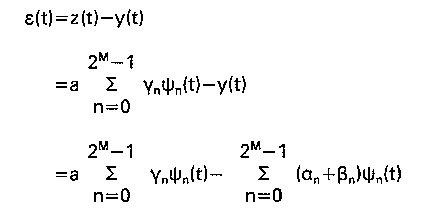
- Continuing with the analysis, the mean squared error for the ADC may be determined as follows:

- The value of the optimum gain aopt that minimizes the mean square error may be obtained by setting to zero the first derivative with respect to the gain "a" and solving for "a" which by substitution becomes:

- The value for the optimum gain can therefore be computed by straightforward numerical computation techniques.
- Linearity error can also be determined as follows: The binary weights of the modified Walsh functions due to the reference DAC outputs are first determined, the linearity error due to the reference DAC is determined and subtracted from each of the binary weights, and then the linearity function is compared with the excitation function, which is typically a maximum entropy function such as a ramp function wherein the contribution to observe linearity error due to the dither signal can be made negligible if synthesized from Walsh functions not used in the test pattern. The binary weights are defined as follows:

- The ideal staircase or ramp function (i.e., uniformly quantized linear function) is expressed as follows:


- The technique for generating the offset error in a tester according to the invention for analog-to-digital converters involves subtracting the known input offsets from the expected mean output level. The offset error, which should ideally be adjusted to zero initially is thus computed from the expression:

- The dither function v(t) is not essential and therefore the coefficient β can be omitted without loss of generality.
- One method by which a DAC could be tested according to the invention is to substitute a DAC to be tested in place of the
reference DAC 20 in the devices disclosed in the embodiment of Figure 3 where theADC 44 has already been characterized by the methods outlined hereinabove. All computations are then referenced to the known responses of the ADC to an expected input signal. Deviations from the expected signal define the coefficients by which the DAC under test can be calibrated. - E. A. Sloane, Fairchild, A. Schlumberger Company, Test Systems Group, San Jose, California 95110.
- A brief introduction to Walsh function leads into a discussion on the generation of maximum entropy sequences for the excitation of the device under test (DUT). A theoretical development relates the Walsh function expansions of the DUT response to converter offset, gain and linearity errors. A procedure for testing is also outlined.
- Walsh functions are a relatively new set of complete orthogonal basis functions that are capable of representing any reasonably well behaved function on a finite interval.
- The essential properties of the Walsh functions may be summarized as follows:
- 1. They are "square" waves that assume value of +/-1.
- 2. The analysis interval is always subdivided into binary subintervals (2").
- 3. The expansion of a function on an analysis interval which is subdivided into 2" sub-intervals may require up to 2" unique Walsh functions.
- 4. Walsh functions are orthogonal.
- 5. Walsh functions are readily generated.
- Figure 1 shows three sets of Walsh functions, {ψk}, of rank two, four or eight which are suitable for expanding functions with two, four or eight terms. The subscript associated with each tp represents the order of the function. Thus, the number of intervals determines the rank; the rank is equal to the total number of Walsh functions; and the order must be less than the rank.
- Note that the Walsh functions of binary order, ψ2k, are simple periodic "square" waves and are the basic kernels from which all other members of a given rank may be generated. The generating algorithm is


- The Walsh functions are orthogonal because

- This means that if a function, x(t), can be expanded into Walsh functions then

- The Walsh coefficients can then be extracted from x(t) as follows:


- The traditional Walsh function theory has been based on continuous functions of time. Even though we will be dealing with sampled time functions also, the basic theory is applicable but invokes sampled Walsh functions instead as shown in Figure 2, where + implies +1 and - implies -1.
- In the sampled case, summations replace integrals so that


- Both the discrete and continuous forms will be useful.
- An additional method for cataloging Walsh functions is by their "sequency" order or by the number of zero crossings within the interval. For example, ψ0 will have no zero crossings while ψ2 has three. Each Walsh function will have a unique sequency number. The binary sequency numbers for rank-16 are shown in Figure 2.
- The similarity to Fourier Series also carries over to a fast Walsh transform (FWT) analogous to the well known fast Fourier transforms except that all multiplications are replaced by additions or subtractions.
- Figure 3, graphically depicts, by means of signal flow diagrams, the FWT process for ranks 2, 4, and 8. The number of adds and subtracts is k · 2" where 2k is the rank.
- The binary numbers at the top indicate the data sample number ranging from 0 to 2k-1. The lower numbers at the output of the transform process, give the order of Walsh coefficients. Note that these coefficients are in a "scrambled" reverse binary order, i.e., 100 and 001 are interchange, for example. If however, the data points are placed in reverse binary scrambled form, then the transformed coefficients will be in normal order.
- The most important class of dynamic test functions is the "maximum entropy" set that has a uniform distribution of values on the interval spanned by the converter under test. For example, the uniform ramp 00...000, 00...001, 00...011, 00...100, 00...101, ..., 11...100, 11...101, 11...110, 11...111, would be a member of this set as well as all other functions that pass through each possible binary code only once for the duration of a rank. For a k-bit function, there are 2"! members in this set.
- If Walsh functions are used to represent the individual bit patterns it is possible to synthesize these patterns by following a simple set of rules. However, it will be convenient to define a modified Walsh function as

 represents the "exclusive-or" operation.
- Note, however, that the modified Walsh functions are not an orthogonal set, because of their non-zero mean.
- The rule for generating a maximum entropy test signal with uniformly distributed values is based on the following conjecture:
- "Given a set of m distinct non-zero order Walsh functions, each with distinct binary weights, the sum of the weighted functions will be a maximum entropy sequence if the mod-2 sum of their Walsh sequency number is not zero and/also if the sequency numbers when "or'd" bit-by-bit is true for all bits".
- Thus, if it is desired to synthesize a maximum entropy, rank-16 function, we must choose 4 Walsh functions (corresponding to 4 bits) that satisfy the above conditions, for example, the set
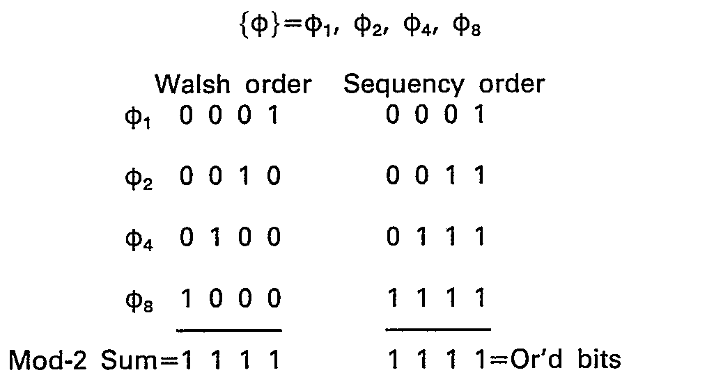
- Both conditions are satisfied, and not unexpectedly because these four functions may be used to form the basic ramp.
- Consider the following:

- The form or the function is evaluated in the following table:

- If all of the 0's were complemented, then


- Note that complementing the Walsh functions reversed the order of the function. This is true because all of the φ's in this example have odd symmetry about the mid-point.
- In general, time-reversal can be achieved by logically complementing only the 0's with odd symmetry about their mid-points.
- For example, consider the following rank-8 functions (Figure 4a and 4b).


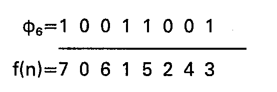


- If the entire function is complemented, the 2m-1 complement is obtained (Figure 4c).
- If




- This rank-8 function could be further permuted by additional selective complementing as well as reassigning binary weights.
- For a final example consider


- Note that this function, shown in Figure 4d, has assumed a "more random" appearance.
- Let the input signal to a converter be synthesized from a set of M binary weighted modified Walsh functions of rank 2M, so that


- Given the input and output of the converter, the mean-squared error, e2, can be found.

- Substituting the previous two expressions for x(t) and y(t) yields

- The value of gain, aopt, that minimizes the M.S. error may be obtained by setting


- The minimum M.S. error, ]


- The linearity error of the converter, ε1, may be obtained by taking the difference between the converter transfer characteristic and the ideal staircase ramp.


- Note that the linearity error does not contain all of the Walsh terms that may contribute to the total M.S.E. but only includes those associated with the binary weights of the linear ramp.
- Finally, the converter offset may be obtained by measuring the mean error, E, in the converter output.


- If this offset is removed prior to calculating the optimum gain, it will further reduce the M.S. error.
- The outlined theory forms the basis for calibrating a DAC because the excitation signal is digital and hence is a near perfect drive signal. The response signal can be analyzed either by means of analog or digital processing techniques. Once characterized, the DAC can be used as a reference source for ADC testing using digital processing techniques.
- The potential advantages of this technique include:
- 1. A simple dynamic calibration technique for the reference DAC.
- 2. A simple method for generating maximum entropy test signals that exercise each possible code.
- 3. Dynamic testing of converters allows for detecting "history" dependent or data dependent errors that are not now detected in test.
- 4. Test time is minimized because all weights are evaluated simultaneously.
- The current state-of-the-art, based on static tests, or limited dynamic test techniques such as servo-controlled "dither" detection of transition voltages, leads to inadequate testing and long test times.
- On the other hand, the dynamic Walsh function calibration technique of exciting individual bits of a DAC with orthogonal functions allows for the sorting of each weight's contribution, while dynamically exercising the device under test. Having calibrated the reference DAC, it is possible to generate a "calibrated" dynamic signal for testing either DAC's or ADC's that covers their full dynamic range.
- "Advanced Analytical and Signal Processing Techniques: Application of Walsh Functions to Nonlinear Analysis", M. S. Corrington and R. N. Adams, Technical Report, ASTIA No. AD-277942, 1962.
- "The Walsh Functions", N. J. Fine, Encyclopedic Dictionary of Physics, Pergamon Press, Oxford, 1969.
- "The Generalized Walsh Functions", N. J. Fine, Transactions of Am. Math. Soc., vol. 69, pp. 66-77, 1950.
- "On the Walsh Functions", N. J. Fine, Transactions of Am. Math. Soc., vol. 65, pp. 372-414, 1949.
- "Testing Digital/Analog and Analog/Digital Converters", J. R. Naylor, IEEE Trans. Circuits and Systems, vol. CAS-25, No. 7, pp. 526-538, July 1978.
- "Designing an Analog LSI Converter Test System", J. Seaton, B. Webster and P. Oiseau, Electronic Packaging and Production, January, 1980.
- "Computation of the Fast Walsh-Fourier Transform", J. L. Shanks, IEEE Transactions on Computers, pp. 457-459, May, 1969. Also, IEEE Computer Group Repository, R-69-18.
- "Analog-Digital Conversion Notes", D. H. Sheingold, Editor, Analog Devices, Inc., Norwood, Massachusetts, pp. 191-215, 1977.
- "A Closed Set of Orthogonal Functions", J. L. Walsh, Am. Jour. of Math., vol. 45, pp. 5-24, 1923.


Claims (18)
characterized in that said known signal consists of a set of orthogonal digital functions over a defined interval and has its amplitude substantially uniformly distributed among allowable states to approximate a maximum entropy sequence signal; and further characterized by the steps of applying each orthogonal function of a single corresponding set of said known signal to said digital-to-analog converter to generate an excitation signal which varies according to the binary weighting induced by said orthogonal functions; and examining the output signal produced by each bit of said analog-to-digital converter under test by correlating said output response signal with each selected orthogonal function.


characterized in that said digital excitation signal consists of a set of orthogonal functions having a known substantially uniform amplitude probability density function among allowable states for exciting substantially all allowable states of a digital-to-analog converter to which said generated digital excitation signal is applied; and
further characterized by the step of comparing measured coefficients and known coefficients characterizing said processing signal and said response to determine deviation of said output response signal from a computed signal produced by said processing signal.
Applications Claiming Priority (2)
| Application Number | Priority Date | Filing Date | Title |
|---|---|---|---|
| US204979 | 1980-11-07 | ||
| US06/204,979 US4419656A (en) | 1980-11-07 | 1980-11-07 | Method and apparatus for digital converter testing |
Publications (3)
| Publication Number | Publication Date |
|---|---|
| EP0052048A2 EP0052048A2 (en) | 1982-05-19 |
| EP0052048A3 EP0052048A3 (en) | 1982-12-22 |
| EP0052048B1 true EP0052048B1 (en) | 1987-12-02 |
Family
ID=22760274
Family Applications (1)
| Application Number | Title | Priority Date | Filing Date |
|---|---|---|---|
| EP81401721A Expired EP0052048B1 (en) | 1980-11-07 | 1981-10-28 | Method and apparatus for a/d and d/a converter testing |
Country Status (5)
| Country | Link |
|---|---|
| US (1) | US4419656A (en) |
| EP (1) | EP0052048B1 (en) |
| JP (1) | JPS57145431A (en) |
| DE (1) | DE3176559D1 (en) |
| NO (1) | NO160109C (en) |
Cited By (1)
| Publication number | Priority date | Publication date | Assignee | Title |
|---|---|---|---|---|
| DE102005045183A1 (en) * | 2005-09-21 | 2007-03-22 | Infineon Technologies Ag | Test unit for digitized test results and testing an diagnostic method for semiconductor components has reference signal generator and signal extractor |
Families Citing this family (21)
| Publication number | Priority date | Publication date | Assignee | Title |
|---|---|---|---|---|
| DE3218066A1 (en) * | 1981-07-08 | 1983-01-27 | Siemens AG, 1000 Berlin und 8000 München | METHOD FOR TESTING ANALOG-DIGITAL CONVERTERS AND / OR DIGITAL-ANALOG CONVERTERS OR MESSAGE-TECHNICAL TRANSMISSION SECTIONS THAT CONTAIN SUCH CONVERTERS OR ARE IN SERIES WITH THEM, ESPECIALLY TO MAKE A CUTTER PROCEDURE |
| US4758781A (en) * | 1985-12-06 | 1988-07-19 | Hitachi, Ltd. | DA converter testing system |
| US4679028A (en) * | 1986-03-31 | 1987-07-07 | Motorola Inc. | Fault detection algorithm for successive-approximation A/D converters |
| JPS63224525A (en) * | 1987-03-13 | 1988-09-19 | Yokogawa Electric Corp | Device for evaluating d/a converter |
| JPS63227122A (en) * | 1987-03-16 | 1988-09-21 | Yokogawa Electric Corp | D/a converter evaluating device |
| US4839651A (en) * | 1987-07-24 | 1989-06-13 | Hewlett-Packard Company | Apparatus for measuring the dynamic characteristics of an analog-digital converter |
| US5043931A (en) * | 1989-06-19 | 1991-08-27 | International Business Machines Corporation | Wrap test system and method |
| JP2705596B2 (en) * | 1994-11-29 | 1998-01-28 | 日本電気株式会社 | Test method for digital / analog converter |
| US5659312A (en) * | 1996-06-14 | 1997-08-19 | Logicvision, Inc. | Method and apparatus for testing digital to analog and analog to digital converters |
| US5861826A (en) * | 1997-06-30 | 1999-01-19 | Harris Corporation | Method and apparatus for calibrating integrated circuit analog-to-digital converters |
| US6259389B1 (en) * | 1998-11-20 | 2001-07-10 | General Electric Company | System for designing and testing a sigma-delta modulator using response surface techniques |
| US6232759B1 (en) * | 1999-10-21 | 2001-05-15 | Credence Systems Corporation | Linear ramping digital-to-analog converter for integrated circuit tester |
| EP1102403A1 (en) * | 1999-11-19 | 2001-05-23 | ABB Power Automation AG | Operation monitoring for a transformer |
| US6781531B2 (en) * | 2002-01-15 | 2004-08-24 | Raytheon Company | Statistically based cascaded analog-to-digital converter calibration technique |
| WO2004030219A1 (en) * | 2002-09-27 | 2004-04-08 | Analog Devices, Inc. | System and method for digital compensation of digital to analog and analog to digital converters |
| JP4315663B2 (en) * | 2002-10-17 | 2009-08-19 | ユニチカ株式会社 | Method for producing nonwoven fabric comprising core-sheath composite long fiber |
| US7081841B1 (en) * | 2005-04-28 | 2006-07-25 | Lsi Logic Corporation | Analog to digital converter built in self test |
| JP4435197B2 (en) * | 2007-03-29 | 2010-03-17 | 株式会社東芝 | Semiconductor integrated circuit |
| CN101491386B (en) * | 2009-03-06 | 2011-04-06 | 陈佳燕 | Curling comb with rotary drum |
| US8314725B2 (en) * | 2010-09-15 | 2012-11-20 | Intel Corporation | On-die digital-to-analog conversion testing |
| CN103067009A (en) * | 2012-12-27 | 2013-04-24 | 东南大学 | High-precision digital analog converter test system |
Family Cites Families (1)
| Publication number | Priority date | Publication date | Assignee | Title |
|---|---|---|---|---|
| JPS5240011A (en) * | 1975-09-25 | 1977-03-28 | Matsushita Electric Ind Co Ltd | Orthogonal converting device |
-
1980
- 1980-11-07 US US06/204,979 patent/US4419656A/en not_active Expired - Lifetime
-
1981
- 1981-10-28 DE DE8181401721T patent/DE3176559D1/en not_active Expired
- 1981-10-28 EP EP81401721A patent/EP0052048B1/en not_active Expired
- 1981-10-29 NO NO813668A patent/NO160109C/en unknown
- 1981-11-07 JP JP56178903A patent/JPS57145431A/en active Pending
Cited By (3)
| Publication number | Priority date | Publication date | Assignee | Title |
|---|---|---|---|---|
| DE102005045183A1 (en) * | 2005-09-21 | 2007-03-22 | Infineon Technologies Ag | Test unit for digitized test results and testing an diagnostic method for semiconductor components has reference signal generator and signal extractor |
| US7720645B2 (en) | 2005-09-21 | 2010-05-18 | Infineon Technologies Ag | Test apparatus for digitized test responses, method for testing semiconductor devices and diagnosis method for a semiconductor device |
| DE102005045183B4 (en) * | 2005-09-21 | 2011-03-31 | Infineon Technologies Ag | Test device and method for evaluating a digitized test response |
Also Published As
| Publication number | Publication date |
|---|---|
| DE3176559D1 (en) | 1988-01-14 |
| US4419656A (en) | 1983-12-06 |
| EP0052048A2 (en) | 1982-05-19 |
| EP0052048A3 (en) | 1982-12-22 |
| NO813668L (en) | 1982-05-10 |
| JPS57145431A (en) | 1982-09-08 |
| NO160109B (en) | 1988-11-28 |
| NO160109C (en) | 1989-03-08 |
Similar Documents
| Publication | Publication Date | Title |
|---|---|---|
| EP0052048A2 (en) | Method and apparatus for A/D and D/A converter testing | |
| Bossche et al. | Dynamic testing and diagnostics of A/D converters | |
| EP0066504B1 (en) | Method for analyzing a digital-to-analog converter with nonideal analog-to-digital converter | |
| EP0071539B1 (en) | Method and apparatus for calibrating an analog-to-digital converter for a digital-to-analog converter test system | |
| Pan et al. | Pseudorandom testing for mixed-signal circuits | |
| Vanden Bossche et al. | Dynamic testing and diagnostics of A/D converters | |
| Attivissimo et al. | INL reconstruction of A/D converters via parametric spectral estimation | |
| US4667296A (en) | Testing the transfer function linearity of analogue input circuits | |
| US4465995A (en) | Method and apparatus for analyzing an analog-to-digital converter with a nonideal digital-to-analog converter | |
| Aliev et al. | On inversion of Bessel potentials associated with the Laplace–Bessel differential operator | |
| EP0308599A2 (en) | Digitizer effective resolution measurement system using estimated sinewave parameters | |
| Mikulik et al. | Volterra filtering for integrating ADC error correction, based on an a priori error model | |
| JP2002031670A (en) | Apparatus and method including efficient data transmission for testing a/d converter | |
| EP0293285A1 (en) | A method for determining transfer characteristics of an AC calibration device | |
| Reed et al. | Practical modeling of nonlinear audio systems using the volterra series | |
| Max | Ramp testing of ADC transition levels using finite resolution ramps | |
| Grimaldi et al. | Identification of ADC error model by testing of the chosen code bins | |
| US4583075A (en) | Method and apparatus for analyzing an analog-to-digital converter with a nonideal digital-to-analog converter | |
| Gamad et al. | Gain error, offset error and ENOB estimation of an A/D converter using histogram technique | |
| EP0626763B1 (en) | Method and apparatus for converting an analog signal to a digital floating-point number and a digital floating-pont number to an analog signal | |
| Mansour et al. | Design and implementation of a platform for experimental testing and validation of analog-to-digital converters: static and dynamic parameters | |
| Ming | Modeling the harmonic distortion of analog-to-digital converter using Volterra series | |
| Brygilewicz et al. | Time-domain fault diagnosis of analogue circuits in the presence of noise | |
| Lu et al. | A Digital Calibration Technique for Frequency Response Mismatches in M-Channel Time-Interleaved ADCs Based on Taylor Approximation | |
| Mishra et al. | Determination of Nonlinearity and Effective Resolution of an A/D Converter for Arbitrary Application Input |
Legal Events
| Date | Code | Title | Description |
|---|---|---|---|
| PUAI | Public reference made under article 153(3) epc to a published international application that has entered the european phase |
Free format text: ORIGINAL CODE: 0009012 |
|
| AK | Designated contracting states |
Designated state(s): BE DE FR GB IT NL SE |
|
| PUAL | Search report despatched |
Free format text: ORIGINAL CODE: 0009013 |
|
| AK | Designated contracting states |
Designated state(s): BE DE FR GB IT NL SE |
|
| 17P | Request for examination filed |
Effective date: 19830618 |
|
| GRAA | (expected) grant |
Free format text: ORIGINAL CODE: 0009210 |
|
| ITF | It: translation for a ep patent filed | ||
| AK | Designated contracting states |
Kind code of ref document: B1 Designated state(s): BE DE FR GB IT NL SE |
|
| REF | Corresponds to: |
Ref document number: 3176559 Country of ref document: DE Date of ref document: 19880114 |
|
| ET | Fr: translation filed | ||
| PLBE | No opposition filed within time limit |
Free format text: ORIGINAL CODE: 0009261 |
|
| STAA | Information on the status of an ep patent application or granted ep patent |
Free format text: STATUS: NO OPPOSITION FILED WITHIN TIME LIMIT |
|
| 26N | No opposition filed | ||
| PGFP | Annual fee paid to national office [announced via postgrant information from national office to epo] |
Ref country code: FR Payment date: 19900922 Year of fee payment: 10 |
|
| PGFP | Annual fee paid to national office [announced via postgrant information from national office to epo] |
Ref country code: GB Payment date: 19900925 Year of fee payment: 10 |
|
| PGFP | Annual fee paid to national office [announced via postgrant information from national office to epo] |
Ref country code: SE Payment date: 19900926 Year of fee payment: 10 |
|
| PGFP | Annual fee paid to national office [announced via postgrant information from national office to epo] |
Ref country code: BE Payment date: 19901010 Year of fee payment: 10 |
|
| ITTA | It: last paid annual fee | ||
| PGFP | Annual fee paid to national office [announced via postgrant information from national office to epo] |
Ref country code: NL Payment date: 19901031 Year of fee payment: 10 |
|
| PGFP | Annual fee paid to national office [announced via postgrant information from national office to epo] |
Ref country code: DE Payment date: 19901228 Year of fee payment: 10 |
|
| PG25 | Lapsed in a contracting state [announced via postgrant information from national office to epo] |
Ref country code: GB Effective date: 19911028 |
|
| PG25 | Lapsed in a contracting state [announced via postgrant information from national office to epo] |
Ref country code: SE Effective date: 19911029 |
|
| PG25 | Lapsed in a contracting state [announced via postgrant information from national office to epo] |
Ref country code: BE Effective date: 19911031 |
|
| BERE | Be: lapsed |
Owner name: FAIRCHILD CAMERA & INSTRUMENT CORP. Effective date: 19911031 |
|
| PG25 | Lapsed in a contracting state [announced via postgrant information from national office to epo] |
Ref country code: NL Effective date: 19920501 |
|
| NLV4 | Nl: lapsed or anulled due to non-payment of the annual fee | ||
| GBPC | Gb: european patent ceased through non-payment of renewal fee | ||
| PG25 | Lapsed in a contracting state [announced via postgrant information from national office to epo] |
Ref country code: FR Effective date: 19920630 |
|
| PG25 | Lapsed in a contracting state [announced via postgrant information from national office to epo] |
Ref country code: DE Effective date: 19920701 |
|
| REG | Reference to a national code |
Ref country code: FR Ref legal event code: ST |
|
| EUG | Se: european patent has lapsed |
Ref document number: 81401721.6 Effective date: 19920510 |