EP0051774A1 - Battery saving frequency synthesizer arrangement - Google Patents
Battery saving frequency synthesizer arrangement Download PDFInfo
- Publication number
- EP0051774A1 EP0051774A1 EP81108771A EP81108771A EP0051774A1 EP 0051774 A1 EP0051774 A1 EP 0051774A1 EP 81108771 A EP81108771 A EP 81108771A EP 81108771 A EP81108771 A EP 81108771A EP 0051774 A1 EP0051774 A1 EP 0051774A1
- Authority
- EP
- European Patent Office
- Prior art keywords
- phase
- vco
- locked loop
- loop
- control signal
- Prior art date
- Legal status (The legal status is an assumption and is not a legal conclusion. Google has not performed a legal analysis and makes no representation as to the accuracy of the status listed.)
- Granted
Links
- 239000003990 capacitor Substances 0.000 claims description 14
- 230000005540 biological transmission Effects 0.000 claims description 8
- 230000008878 coupling Effects 0.000 claims description 7
- 238000010168 coupling process Methods 0.000 claims description 7
- 238000005859 coupling reaction Methods 0.000 claims description 7
- 238000000034 method Methods 0.000 claims description 7
- 230000004044 response Effects 0.000 claims description 7
- 238000004891 communication Methods 0.000 claims description 5
- 238000005070 sampling Methods 0.000 claims description 5
- 230000002194 synthesizing effect Effects 0.000 claims description 4
- 230000003213 activating effect Effects 0.000 claims 1
- 230000000737 periodic effect Effects 0.000 claims 1
- 230000001413 cellular effect Effects 0.000 description 6
- 230000008859 change Effects 0.000 description 4
- 238000010586 diagram Methods 0.000 description 3
- 239000013078 crystal Substances 0.000 description 2
- 238000012986 modification Methods 0.000 description 2
- 230000004048 modification Effects 0.000 description 2
- 230000008901 benefit Effects 0.000 description 1
- 230000008034 disappearance Effects 0.000 description 1
- 230000011664 signaling Effects 0.000 description 1
Images
Classifications
-
- H—ELECTRICITY
- H03—ELECTRONIC CIRCUITRY
- H03L—AUTOMATIC CONTROL, STARTING, SYNCHRONISATION OR STABILISATION OF GENERATORS OF ELECTRONIC OSCILLATIONS OR PULSES
- H03L7/00—Automatic control of frequency or phase; Synchronisation
- H03L7/06—Automatic control of frequency or phase; Synchronisation using a reference signal applied to a frequency- or phase-locked loop
- H03L7/08—Details of the phase-locked loop
- H03L7/14—Details of the phase-locked loop for assuring constant frequency when supply or correction voltages fail or are interrupted
- H03L7/143—Details of the phase-locked loop for assuring constant frequency when supply or correction voltages fail or are interrupted by switching the reference signal of the phase-locked loop
- H03L7/145—Details of the phase-locked loop for assuring constant frequency when supply or correction voltages fail or are interrupted by switching the reference signal of the phase-locked loop the switched reference signal being derived from the controlled oscillator output signal
-
- H—ELECTRICITY
- H04—ELECTRIC COMMUNICATION TECHNIQUE
- H04W—WIRELESS COMMUNICATION NETWORKS
- H04W52/00—Power management, e.g. TPC [Transmission Power Control], power saving or power classes
- H04W52/02—Power saving arrangements
- H04W52/0209—Power saving arrangements in terminal devices
-
- H—ELECTRICITY
- H03—ELECTRONIC CIRCUITRY
- H03L—AUTOMATIC CONTROL, STARTING, SYNCHRONISATION OR STABILISATION OF GENERATORS OF ELECTRONIC OSCILLATIONS OR PULSES
- H03L2207/00—Indexing scheme relating to automatic control of frequency or phase and to synchronisation
- H03L2207/08—Modifications of the phase-locked loop for ensuring constant frequency when the power supply fails or is interrupted, e.g. for saving power
-
- Y—GENERAL TAGGING OF NEW TECHNOLOGICAL DEVELOPMENTS; GENERAL TAGGING OF CROSS-SECTIONAL TECHNOLOGIES SPANNING OVER SEVERAL SECTIONS OF THE IPC; TECHNICAL SUBJECTS COVERED BY FORMER USPC CROSS-REFERENCE ART COLLECTIONS [XRACs] AND DIGESTS
- Y02—TECHNOLOGIES OR APPLICATIONS FOR MITIGATION OR ADAPTATION AGAINST CLIMATE CHANGE
- Y02D—CLIMATE CHANGE MITIGATION TECHNOLOGIES IN INFORMATION AND COMMUNICATION TECHNOLOGIES [ICT], I.E. INFORMATION AND COMMUNICATION TECHNOLOGIES AIMING AT THE REDUCTION OF THEIR OWN ENERGY USE
- Y02D30/00—Reducing energy consumption in communication networks
- Y02D30/70—Reducing energy consumption in communication networks in wireless communication networks
Definitions
- This invention relates generally to high frequency synthesizers.
- High frequency synthesizers are now commonly utilized substitutes for the crystal controlled transmitter oscillators and receiver local oscillators because they are able to provide a frequency stable signal at any one of a plurality of frequencies without the need of a crystal for each such frequency.
- Such synthesizers generally utilize a phase-locked loop including a voltage controlled oscillator (VCO), a reference oscillator, and a phase.detector for comparing the output of the VCO with a reference source.
- VCO voltage controlled oscillator
- reference oscillator Normally, one or more programmable or switchable multipliers or dividers are included within the phase-locked loop so that the loop can be locked to various multiples of the reference source frequency.
- a phase-locked loop synthesizer is considered to include a VCO, a phase-locked loop means, and a reference source.
- the phase-locked loop means includes a phase comparator and perhaps one or more programmable divideres and/or multipliers and a loop (low pass) filter. After appropriate division and/or multiplication, the phase-locked loop means compares the VCO signal output with that of the reference source and provides a loop control signal to the VCO for controlling its frequency.
- a 'memory circuit' functioning as a sample and hold, is coupled between the loop control signal output of the phase-locked loop and the control input of the voltage controlled oscillator.
- This memory circuit comprises a switch for opening and closing the control signal line from the phase-locked loop, a capacitor coupled so as to be charged by the control signal from the phase-locked loop when the switch is closed, and an amplifier having a high impedance input coupling the capacitor and switch to the control input of the voltage controlled oscillator.
- the switch When the switch is closed the loop operates normally and locks. Once the loop has been locked, power to the phase-locked loop can be interrupted.
- the switch is opened and the voltage on the capacitor coupled to the input of the high impedance amplifier becomes the control signal for the voltage controlled oscillator.
- This control signal is equal in magnitude to the control signal from the phase-locked loop just before power to the loop was interrupted.
- the amplifier is selected to have a high input impedance so that the voltage on the capacitor will not discharge very rapidly and the voltage controlled oscillator will be prevented from drifting substantially. Before the voltage controlled oscillator can drift too far, power is reapplied to the phase-locked loop and the switch is again closed so that the loop can be relocked.
- the frequency and duration of power interruptions and attendant switch openings and the various circuit parameters are determined by how severely the loop drifts when unlocked.
- a method for frequency synthesizing using a phase-locked loop synthesizer comprising the steps of: generating, with phase-locked loop means, a loop control signal for use in controlling a voltage controlled oscillator (VCO) associated with the phase-locked loop means; sampling the magnitude of the loop control signal; generating a memory signal indicative of the sampled magnitude of the loop control signal; interrupting power to the phase-locked loop means; and applying the memory signal, simultaneously with the interruption of power, to a control input of the VCO for controlling its frequency during the power interruption.
- VCO voltage controlled oscillator
- phase-locked loop As used in a cellular radio such as a mobile telephone, power to the phase-locked loop is normally interrupted (once the loop has been locked a first time). During the time power is interrupted, the switch of the memory means is open. Periodically power is automatically applied to the phase-locked loop and the switch is closed. In addition, power is continuously applied to the phase-locked loop in response tq (a) a received command to switch frequency (synthesizer must switch to a new frequency) and transmit, or (b) a received command to transmit on the current frequency, (c) an off-hook condition or (d) a loss of a received signal.
- the voltage controlled oscillator is controlled by the output of a receiver discriminator within the communication equipment.
- Switch means are provided for periodically switching the control input of the voltage controlled oscillator away from the loop control signal output of the phase-locked loop means and connecting it instead to the output of the discriainator.
- An integrator is coupled in the loop control signal path to the voltage controlled oscillator.
- the loop is first locked in the conventional manner. Then, the switch means switches the input of the integrator from its normal connection to the phase-locked loop to the output of the discriminator.
- both the phase-locked loop and discriminator must have a zero voltage error signal during a locked condition.
- Properly designed FM receivers with S-type discriminators can produce a DC voltage proportional to the deviation of the local oscillator frequency and the transmitted signal carrier frequency.
- the phase-locked loop need only be relocked in the traditional manner if the received signal is lost or when it is desired to change received channels.
- a method for frequency synthesizing comprising the steps of: generating, with phase-locked loop means, a loop control signal for use in controlling a voltage controlled oscillator (VCO) associated with the phase-locked loop means; locking the phase-locked loop; decoupling the control input of the VCO from the phase-locked loop means and coupling it instead to the output of a receiver discriminator so that the VCO will be controlled by the discriminator output rather than the loop control signal from the phase-locked loop means; and interrupting power to the phase-locked loop means.
- VCO voltage controlled oscillator
- phase-locked loop As used in a cellular radio, such as a mobile telephone, after the phase-locked loop has been initially locked, normally power to the phase-locked loop is disabled. During the time the phase-locked loop is disabled, the voltage controlled oscillator is driven by the receiver discriminator. Power is applied to the phase-locked loop whenever (a) a received command calling to ' a switch in frequency and transmission on the new frequency, (b) a received command calling for transmission on the current frequency, (c) an off-hook condition, or (d) loss of a received signal. A return to the normally disabled (power interrupted) condition of the phase-locked loop occurs in the absence of any of the (a)-(d) conditions above-listed.
- phase-locked loop synthesizers generally include a voltage controlled oscillator (VCO) providing the output of the synthesizer, one or more dividers for dividing the output signal of the voltage controlled oscillator, a phase detector for comparing the direct or derivative (divided) signal from the VCO with a stable signal from a reference source, and a loop filter for receiving the comparison signal from the phase detector and providing a VCO control signal.
- VCO voltage controlled oscillator
- dividers for dividing the output signal of the voltage controlled oscillator
- phase detector for comparing the direct or derivative (divided) signal from the VCO with a stable signal from a reference source
- a loop filter for receiving the comparison signal from the phase detector and providing a VCO control signal.
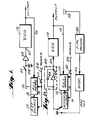
- Phase-locked loop (PLL) 10 represents all of the components of a conventional phase-locked loop synthesizer except for its voltage controlled oscillator (VCO) 12 shown as a separate block.
- the output of phase-locked loop 10 on a signal line 12 represents the loop control signal normally obtained from the loop filter of a phase-locked loop synthesizer.
- phase-locked loop 10 includes a phase comparator for comparing the signal output of VCO 12 with the signal from a reference source 14.
- the phase comparator of PLL 10 receives a signal from reference source 14 on a signal line 16 and the output of VCO 12 on a signal line 18.
- the specific details of the phase-locked loop synthesizer 10 are omitted.
- phase-locked loop frequency synthesizers The details for designing phase-locked loop synthesizers for specific applications can be obtained from a reading of "Frequency Synthesizers Theory and Design. by V. Manassewitsch, published by John Wiley & Sons, copyright 1976.
- Various phase-locked loops suitable for use as phase-locked loop 10 are even available in "off the shelf” integrated circuit packages.
- the loop control signal on line 12 is coupled to one pole of a switch 20.
- the other pole of switch 20 is coupled to a capacitor 22 and to the input of an amplifier 24, the output of which is coupled to the control input 26 of VCO 12.
- the phase-locked loop synthesizer operates as a conventional phase-locked loop when power is applied to PLL 10 and when switch 20 is closed. In this manner, the loop control signal on line 12 is coupled to capacitor 22 and to the input of amplifier 24.
- switch 20 is opened and power to phase-locked loop 10 on a power line 28 is removed.
- the means for interrupting power on line 28 to PLL 10 is symbolized by a switch 60.
- switch 60 would probably be an electronic switch driven by a pulse generator, or other suitable arrangement.
- phase-locked loop 10 is disabled and the power normally drawn thereby is saved.
- the magnitude of the loop control signal on line 12, just before switch 20 is opened, is "memorized" by capacitor 22.
- the input to amplifier 24 is of sufficiently high impedance so that the voltage on capacitor 22 does not discharge substantially during the time interval that phase-locked loop 10 is disabled.
- the value of the loop control signal just before switch 20 is opened continues to be coupled to control input 26 of VCO 12 during the time that phase-locked loop 10 is disabled.
- phase-locked loop 10 is reenergized via switch 60 and switch 20 is closed.
- switches 20 and 60 are operated periodically and synchronously. This allows the loop to relock to relock and reestablish a loop control signal before too much error builds up in the VCO output frequency due to drift.
- FIGURE 1 arrangement is highly suitable for use in a cellular radio such as a mobile telephone.
- power, on line 28 is normally interrupted to PLL 10 (after a period of initial lock).
- switch 20 is opened and VCO 12-is controlled by the signal on capacitor 22.
- PLL 10 is automatically recurrently enabled.
- switch 20 is closed so that the magnitude of the control signal on line 12 is updated by capacitor 22.
- PLL 10 is continuously enabled in response to any of the following conditions:
- phase-locked loop 10 represents all of the phase-locked loop synthesizer components except for the VCO which is shown as a separate block 12.
- the switch for switching between normal and battery saving modes of operation is a single pole double throw switch 40.
- a loop control signal on signal line 12 from phase-locked loop 10 is coupled through switch 40 to the input of an integrator 42.
- the integrator 42 is represented by an amplifier 44 in combination with a feedback capacitor 46.
- the output of integrator 42 is coupled to control input 26 of VCO 12.
- the output of VCO 12 which is the synthesizer output, is coupled on signal line 18 to a phase comparator (or divider) within phase-locked loop 10.
- this second embodiment during battery save operation, the phase-locked loop 10 is held close to lock by an FM receiver 48 and discriminator 50.
- this second embodiment is highly suitable for use in receivers or transceivers in mobile or portable communication.
- phase-locked loop error signal must produce a zero error signal when locked.
- the magnitude of the VCO control signal applied to control input 26 will not change. Only when the signal on line 12 from phase-locked loop 10 deviates from zero will the control input to VCO 12 change.
- a properly designed FM receiver 48 using an S-type discriminator can produce a DC voltage proportional to deviation between its local oscillator frequency and signal frequency as received through it and antenna 52.
- This DC voltage produced by FM receiver 48 and discriminator 50 known as the automatic frequency control (APC) signal is coupled to the second throw of switch 40 and is utilized to control the phase-locked loop during battery save operation.
- APC automatic frequency control
- switch 40 is switched so that the AFC output of discriminator 50 is coupled to the input of integrator 42, and power to phase-locked loop 10 via line 28 is interrupted by the opening of switch 60. During such power interruption periods, the AFC output of discriminator 50 maintains an appropriate control signal on VCO 12 unless the signal received by receiver 48 is lost or until it is desired to change received channels.
- PLL 10 In the context of operation of the FIGURE 2 embodiment in a cellular radio such as a mobile telephone, power to PLL 10 is normally disabled after an initial lock of the phase-locked loop. During times of power interruption to PLL 10, discriminator 50 drives VCO 12. PLL 10 is enabled continuously in response to the occurrence of any of the following conditions:
Landscapes
- Engineering & Computer Science (AREA)
- Computer Networks & Wireless Communication (AREA)
- Signal Processing (AREA)
- Stabilization Of Oscillater, Synchronisation, Frequency Synthesizers (AREA)
Abstract
Description
- This invention relates generally to high frequency synthesizers. High frequency synthesizers are now commonly utilized substitutes for the crystal controlled transmitter oscillators and receiver local oscillators because they are able to provide a frequency stable signal at any one of a plurality of frequencies without the need of a crystal for each such frequency. Such synthesizers generally utilize a phase-locked loop including a voltage controlled oscillator (VCO), a reference oscillator, and a phase.detector for comparing the output of the VCO with a reference source. Normally, one or more programmable or switchable multipliers or dividers are included within the phase-locked loop so that the loop can be locked to various multiples of the reference source frequency.
- As high frequency synthesizers have become widely utilized, they have even been incorporated into portable or mobile battery powered radio communication equipment, such as cellular type radio telephone equipment. It has been found, however, that during normal operation, the phase-locked loop of a synthesizer requires substantial power to operate. Cellular radio equipment must spend large amounts of time receiving a signalling channel. During such reception, the phase-locked loop of its synthesizer is normally continuously operated. Under such operating conditions, the high power drain associated with the synthesizer expends the available battery power in an impractically short period of time.
- In order to overcome the rapid battery drain associated with the continuous use of a phase-locked loop high frequency synthesizer in battery powered radio equipment, there is provided a high frequency synthesizer arrangement utilizing less battery power than conventional arrangements without sacrificing synthesizer performance.
- For ease in discussion and illustration, a phase-locked loop synthesizer is considered to include a VCO, a phase-locked loop means, and a reference source. The phase-locked loop means includes a phase comparator and perhaps one or more programmable divideres and/or multipliers and a loop (low pass) filter. After appropriate division and/or multiplication, the phase-locked loop means compares the VCO signal output with that of the reference source and provides a loop control signal to the VCO for controlling its frequency.
- In a first embodiment of the invention, a 'memory circuit' functioning as a sample and hold, is coupled between the loop control signal output of the phase-locked loop and the control input of the voltage controlled oscillator. This memory circuit comprises a switch for opening and closing the control signal line from the phase-locked loop, a capacitor coupled so as to be charged by the control signal from the phase-locked loop when the switch is closed, and an amplifier having a high impedance input coupling the capacitor and switch to the control input of the voltage controlled oscillator. When the switch is closed the loop operates normally and locks. Once the loop has been locked, power to the phase-locked loop can be interrupted. During such power interruptions, the switch is opened and the voltage on the capacitor coupled to the input of the high impedance amplifier becomes the control signal for the voltage controlled oscillator. This control signal is equal in magnitude to the control signal from the phase-locked loop just before power to the loop was interrupted. The amplifier is selected to have a high input impedance so that the voltage on the capacitor will not discharge very rapidly and the voltage controlled oscillator will be prevented from drifting substantially. Before the voltage controlled oscillator can drift too far, power is reapplied to the phase-locked loop and the switch is again closed so that the loop can be relocked. The frequency and duration of power interruptions and attendant switch openings and the various circuit parameters are determined by how severely the loop drifts when unlocked.
- Thus there is provided a method for frequency synthesizing using a phase-locked loop synthesizer comprising the steps of: generating, with phase-locked loop means, a loop control signal for use in controlling a voltage controlled oscillator (VCO) associated with the phase-locked loop means; sampling the magnitude of the loop control signal; generating a memory signal indicative of the sampled magnitude of the loop control signal; interrupting power to the phase-locked loop means; and applying the memory signal, simultaneously with the interruption of power, to a control input of the VCO for controlling its frequency during the power interruption.
- As used in a cellular radio such as a mobile telephone, power to the phase-locked loop is normally interrupted (once the loop has been locked a first time). During the time power is interrupted, the switch of the memory means is open. Periodically power is automatically applied to the phase-locked loop and the switch is closed. In addition, power is continuously applied to the phase-locked loop in response tq (a) a received command to switch frequency (synthesizer must switch to a new frequency) and transmit, or (b) a received command to transmit on the current frequency, (c) an off-hook condition or (d) a loss of a received signal.
- In an alternative embodiment, during periods of power interruption to the phase-locked loop, the voltage controlled oscillator is controlled by the output of a receiver discriminator within the communication equipment. Switch means are provided for periodically switching the control input of the voltage controlled oscillator away from the loop control signal output of the phase-locked loop means and connecting it instead to the output of the discriainator. An integrator is coupled in the loop control signal path to the voltage controlled oscillator. In this second arrangement, the loop is first locked in the conventional manner. Then, the switch means switches the input of the integrator from its normal connection to the phase-locked loop to the output of the discriminator. Of course, using this arrangement, both the phase-locked loop and discriminator must have a zero voltage error signal during a locked condition. Properly designed FM receivers with S-type discriminators can produce a DC voltage proportional to the deviation of the local oscillator frequency and the transmitted signal carrier frequency. In this second embodiment, the phase-locked loop need only be relocked in the traditional manner if the received signal is lost or when it is desired to change received channels.
- Thus, there is provided a method for frequency synthesizing comprising the steps of: generating, with phase-locked loop means, a loop control signal for use in controlling a voltage controlled oscillator (VCO) associated with the phase-locked loop means; locking the phase-locked loop; decoupling the control input of the VCO from the phase-locked loop means and coupling it instead to the output of a receiver discriminator so that the VCO will be controlled by the discriminator output rather than the loop control signal from the phase-locked loop means; and interrupting power to the phase-locked loop means.
- As used in a cellular radio, such as a mobile telephone, after the phase-locked loop has been initially locked, normally power to the phase-locked loop is disabled. During the time the phase-locked loop is disabled, the voltage controlled oscillator is driven by the receiver discriminator. Power is applied to the phase-locked loop whenever (a) a received command calling to' a switch in frequency and transmission on the new frequency, (b) a received command calling for transmission on the current frequency, (c) an off-hook condition, or (d) loss of a received signal. A return to the normally disabled (power interrupted) condition of the phase-locked loop occurs in the absence of any of the (a)-(d) conditions above-listed.
- The invention will become better understood by reference to the following detailed description and the appended claims when read in conjunction with the Figures, wherein:
- FIGURE 1 is a block diagram of a first embodiment of the frequency synthesizer arrangement according to the present invention; and
- FIGURE 2 is a block diagram of a second embodiment of the frequency synthesizer arrangement according to the present invention.
- Referring now to FIGURE 1, there is shown a first embodiment of the battery saving frequency synthesizer circuit according to the present invention. As previously stated, phase-locked loop synthesizers generally include a voltage controlled oscillator (VCO) providing the output of the synthesizer, one or more dividers for dividing the output signal of the voltage controlled oscillator, a phase detector for comparing the direct or derivative (divided) signal from the VCO with a stable signal from a reference source, and a loop filter for receiving the comparison signal from the phase detector and providing a VCO control signal. By changing the divide ratio of the dividers, various multiples of the reference oscillator frequency can be locked onto by the phase-locked loop.
- Phase-locked loop (PLL) 10 represents all of the components of a conventional phase-locked loop synthesizer except for its voltage controlled oscillator (VCO) 12 shown as a separate block. The output of phase-locked
loop 10 on asignal line 12 represents the loop control signal normally obtained from the loop filter of a phase-locked loop synthesizer. Thus, phase-lockedloop 10 includes a phase comparator for comparing the signal output ofVCO 12 with the signal from areference source 14. In essence, the phase comparator ofPLL 10 receives a signal fromreference source 14 on asignal line 16 and the output ofVCO 12 on asignal line 18. For the purposes of this description, the specific details of the phase-lockedloop synthesizer 10 are omitted. The invention has general application to all phase-locked loop frequency synthesizers. The details for designing phase-locked loop synthesizers for specific applications can be obtained from a reading of "Frequency Synthesizers Theory and Design. by V. Manassewitsch, published by John Wiley & Sons, copyright 1976. Various phase-locked loops suitable for use as phase-lockedloop 10 are even available in "off the shelf" integrated circuit packages. - The loop control signal on
line 12 is coupled to one pole of aswitch 20. The other pole ofswitch 20 is coupled to a capacitor 22 and to the input of anamplifier 24, the output of which is coupled to the control input 26 ofVCO 12. - The phase-locked loop synthesizer operates as a conventional phase-locked loop when power is applied to
PLL 10 and whenswitch 20 is closed. In this manner, the loop control signal online 12 is coupled to capacitor 22 and to the input ofamplifier 24. During "battery save" operation,switch 20 is opened and power to phase-lockedloop 10 on apower line 28 is removed. The means for interrupting power online 28 toPLL 10 is symbolized by aswitch 60. Of course, in a practical design,switch 60 would probably be an electronic switch driven by a pulse generator, or other suitable arrangement. During the time when power is interrupted toPLL 10 viaswitch 60 andswitch 10 is open. power is maintained toVCO 12 andamplifier 24. Thus, during battery save operation, phase-lockedloop 10 is disabled and the power normally drawn thereby is saved. The magnitude of the loop control signal online 12, just beforeswitch 20 is opened, is "memorized" by capacitor 22. The input toamplifier 24 is of sufficiently high impedance so that the voltage on capacitor 22 does not discharge substantially during the time interval that phase-lockedloop 10 is disabled. Thus, the value of the loop control signal just beforeswitch 20 is opened continues to be coupled to control input 26 ofVCO 12 during the time that phase-lockedloop 10 is disabled. Periodically, phase-lockedloop 10 is reenergized viaswitch 60 andswitch 20 is closed. Thus switches 20 and 60 are operated periodically and synchronously. This allows the loop to relock to relock and reestablish a loop control signal before too much error builds up in the VCO output frequency due to drift. - This FIGURE 1 arrangement is highly suitable for use in a cellular radio such as a mobile telephone. Operated in a mobile telephone, power, on
line 28, is normally interrupted to PLL 10 (after a period of initial lock). During the time when power toPLL 10 is disabled, switch 20 is opened and VCO 12-is controlled by the signal on capacitor 22.PLL 10 is automatically recurrently enabled. During such time of enablement, switch 20 is closed so that the magnitude of the control signal online 12 is updated by capacitor 22.PLL 10 is continuously enabled in response to any of the following conditions: - (a) a received command indicating a switch in frequency and transmission on the new frequency,
- (b) a received command calling for a transmission on the current frequency,
- (c) an off-hook condition, or
- (d) the loss of a received signal.
- Referring now to FIGURE 2, there is shown a block diagram of a second embodiment of the battery saving frequency synthesizer circuit according to the present invention. As in FIGURE 1 phase-locked
loop 10 represents all of the phase-locked loop synthesizer components except for the VCO which is shown as aseparate block 12. In this second embodiment, the switch for switching between normal and battery saving modes of operation is a single poledouble throw switch 40. In normal operation (non-battery save), a loop control signal onsignal line 12 from phase-lockedloop 10 is coupled throughswitch 40 to the input of an integrator 42. The integrator 42 is represented by an amplifier 44 in combination with a feedback capacitor 46. However, other integrators will serve the same purpose. The output of integrator 42 is coupled to control input 26 ofVCO 12. At in the FIGURE 1 embodiment, the output ofVCO 12, which is the synthesizer output, is coupled onsignal line 18 to a phase comparator (or divider) within phase-lockedloop 10. - In this second embodiment, during battery save operation, the phase-locked
loop 10 is held close to lock by anFM receiver 48 and discriminator 50. Thus, this second embodiment is highly suitable for use in receivers or transceivers in mobile or portable communication. - Because the loop control signal of
signal 12 from phase-lockedloop 10 is coupled to control input 26 of theVCO 12 through an integrator 42, the phase-locked loop error signal must produce a zero error signal when locked. Thus, when locked, the magnitude of the VCO control signal applied to control input 26 will not change. Only when the signal online 12 from phase-lockedloop 10 deviates from zero will the control input toVCO 12 change. - A properly designed
FM receiver 48 using an S-type discriminator can produce a DC voltage proportional to deviation between its local oscillator frequency and signal frequency as received through it andantenna 52. This DC voltage produced byFM receiver 48 and discriminator 50, known as the automatic frequency control (APC) signal is coupled to the second throw ofswitch 40 and is utilized to control the phase-locked loop during battery save operation. - During battery save operation, switch 40 is switched so that the AFC output of discriminator 50 is coupled to the input of integrator 42, and power to phase-locked
loop 10 vialine 28 is interrupted by the opening ofswitch 60. During such power interruption periods, the AFC output of discriminator 50 maintains an appropriate control signal onVCO 12 unless the signal received byreceiver 48 is lost or until it is desired to change received channels. - In the context of operation of the FIGURE 2 embodiment in a cellular radio such as a mobile telephone, power to
PLL 10 is normally disabled after an initial lock of the phase-locked loop. During times of power interruption toPLL 10, discriminator 50drives VCO 12.PLL 10 is enabled continuously in response to the occurrence of any of the following conditions: - (a) a received command calling for a switch in frequency and transmission on the new frequency,
- (b) a received comand calling for transmission on the current frequency,
- (c) an off-hook condition or
- (d) the loss of a received signal.
- Thus, there has been provided a frequency synthesizer circuit arrangement highly suitable for mobile or portable use. During extended periods of time, power to the phase-locked loop is disabled thereby considerably extending battery life.
- Of course, other alternative embodiments and modifications of the present invention will be apparent to those of ordinary skill in the art having the benefit of the teachings contained herein. Therefore, such alternate embodiments and modifications are intended to be covered within the scope of the appended claims.
In the absence of any of conditions (a) through (d), above, the synthesizer is returned to its normally PLL disabled state with
The synthesizer is returned to its normally PLL disabled stated with discriminator control of
Claims (12)
whenever power to the phase-locked loop synthesizer means is interrupted, whereby the frequency of the VCO is controlled by the receiver discriminator signal during periods of power interruption to the phase-locked loop synthesizer means.
Applications Claiming Priority (2)
| Application Number | Priority Date | Filing Date | Title |
|---|---|---|---|
| US06/205,516 US4521918A (en) | 1980-11-10 | 1980-11-10 | Battery saving frequency synthesizer arrangement |
| US205516 | 2005-08-17 |
Publications (2)
| Publication Number | Publication Date |
|---|---|
| EP0051774A1 true EP0051774A1 (en) | 1982-05-19 |
| EP0051774B1 EP0051774B1 (en) | 1985-09-11 |
Family
ID=22762514
Family Applications (1)
| Application Number | Title | Priority Date | Filing Date |
|---|---|---|---|
| EP81108771A Expired EP0051774B1 (en) | 1980-11-10 | 1981-10-23 | Battery saving frequency synthesizer arrangement |
Country Status (5)
| Country | Link |
|---|---|
| US (1) | US4521918A (en) |
| EP (1) | EP0051774B1 (en) |
| JP (1) | JPS57109428A (en) |
| HK (1) | HK2289A (en) |
| SG (1) | SG57288G (en) |
Cited By (10)
| Publication number | Priority date | Publication date | Assignee | Title |
|---|---|---|---|---|
| FR2535545A1 (en) * | 1982-10-29 | 1984-05-04 | Thomson Csf | Fast acquisition time frequency synthesizer and frequency hopping radio transmission system containing such a synthesizer. |
| US4598258A (en) * | 1984-06-25 | 1986-07-01 | Nec Corporation | Circuit arrangement comprising a voltage-controlled oscillator operable with different sensitivities |
| EP0186854A2 (en) * | 1984-12-28 | 1986-07-09 | Fujitsu Limited | Frequency synthesizer having means for suppressing frequency instability caused by intermittent PLL operation |
| EP0209321A2 (en) * | 1985-07-15 | 1987-01-21 | Nec Corporation | Phase-locked loop frequency synthesizer |
| EP0228875A1 (en) * | 1985-12-20 | 1987-07-15 | Nec Corporation | Amplifier circuit having short rise-time |
| EP0299674A2 (en) * | 1987-07-11 | 1989-01-18 | Plessey Overseas Limited | Improvements in or relating to frequency synthesisers |
| EP0438260A2 (en) * | 1990-01-19 | 1991-07-24 | Motorola, Inc. | Capacitor precharge for reduced synthesizer lock time |
| EP0735642A1 (en) * | 1995-03-29 | 1996-10-02 | Nec Corporation | Power supply circuit having an auxiliary power source for compensating for main power drop |
| EP0863617A1 (en) * | 1997-03-04 | 1998-09-09 | Koninklijke Philips Electronics N.V. | Transmission system comprising at least one satellite station with circuits powered from a power source |
| WO2001086815A2 (en) * | 2000-05-09 | 2001-11-15 | Qualcomm Incorporated | Method and apparatus for reducing pll lock time |
Families Citing this family (37)
| Publication number | Priority date | Publication date | Assignee | Title |
|---|---|---|---|---|
| US4631496A (en) * | 1981-04-06 | 1986-12-23 | Motorola, Inc. | Battery saving system for a frequency synthesizer |
| JPS61258529A (en) * | 1985-05-13 | 1986-11-15 | Nec Corp | Frequency synthesizer |
| US4733100A (en) * | 1987-01-14 | 1988-03-22 | Fox Technology, Inc. | Automatic on/off circuit with time delay |
| JPS6486739A (en) * | 1987-09-29 | 1989-03-31 | Toshiba Corp | Car telephone equipment |
| US5029237A (en) * | 1988-06-30 | 1991-07-02 | At&E Corporation | Radio receiver frequency control system |
| US4944025A (en) * | 1988-08-09 | 1990-07-24 | At&E Corporation | Direct conversion FM receiver with offset |
| US4955075A (en) * | 1988-10-17 | 1990-09-04 | Motorola, Inc. | Battery saver circuit for a frequency synthesizer |
| US5214795A (en) * | 1989-06-29 | 1993-05-25 | Seiko Corp. | Low voltage automatic frequency control switch for a radio receiver |
| US5335365A (en) * | 1991-07-08 | 1994-08-02 | Motorola, Inc. | Frequency synthesizer with VCO output control |
| US5249233A (en) * | 1992-04-06 | 1993-09-28 | Ford Motor Company | Multipath noise minimizer for radio receiver |
| US5408685A (en) * | 1992-04-06 | 1995-04-18 | Ford Motor Company | Multipath detector using phase comparison of stereo pilot signal |
| JP3146673B2 (en) * | 1992-09-17 | 2001-03-19 | 日本電気株式会社 | FSK receiver |
| US5418503A (en) * | 1993-03-08 | 1995-05-23 | Ericsson Ge Mobile Communications Inc. | Compensation of transient frequency drift in oscillator circuits |
| JPH07105739B2 (en) * | 1993-06-08 | 1995-11-13 | 日本電気株式会社 | Receiving machine |
| DE4329898A1 (en) | 1993-09-04 | 1995-04-06 | Marcus Dr Besson | Wireless medical diagnostic and monitoring device |
| GB2289174B (en) * | 1993-11-09 | 1998-08-19 | Motorola Inc | Apparatus and method for enabling elements of a phase locked loop |
| US6310927B1 (en) * | 1994-03-31 | 2001-10-30 | Stmicroelectronics, Inc. | First order tuning circuit for a phase-locked loop |
| US5748103A (en) * | 1995-11-13 | 1998-05-05 | Vitalcom, Inc. | Two-way TDMA telemetry system with power conservation features |
| US5828954A (en) * | 1996-04-04 | 1998-10-27 | Lucent Technologies Inc. | Transmission system for digital audio broadcasting |
| US5920233A (en) * | 1996-11-18 | 1999-07-06 | Peregrine Semiconductor Corp. | Phase locked loop including a sampling circuit for reducing spurious side bands |
| US6223061B1 (en) * | 1997-07-25 | 2001-04-24 | Cleveland Medical Devices Inc. | Apparatus for low power radio communications |
| AU7758298A (en) * | 1998-04-09 | 1999-11-01 | Nokia Networks Oy | Node control unit of an access node in a telecommunications network |
| US6449485B1 (en) * | 1999-01-22 | 2002-09-10 | International Business Machines Corporation | Technique for mobile wireless device location |
| US6603361B1 (en) * | 1999-12-30 | 2003-08-05 | Stmicroelectronics, Inc. | Method and apparatus for maintaining clock accuracy at power down |
| US6441747B1 (en) | 2000-04-18 | 2002-08-27 | Motorola, Inc. | Wireless system protocol for telemetry monitoring |
| US6496705B1 (en) | 2000-04-18 | 2002-12-17 | Motorola Inc. | Programmable wireless electrode system for medical monitoring |
| CA2414309C (en) | 2000-07-18 | 2006-10-31 | Motorola, Inc. | Wireless electrocardiograph system and method |
| DE60038679T2 (en) * | 2000-10-10 | 2009-05-07 | Nemerix S.A. | Electronic circuit and RF receiver with energy saving control |
| SE518078C2 (en) * | 2000-10-23 | 2002-08-20 | Spirea Ab | Frequency synthesizer and method for synthesizing a frequency |
| US6456887B1 (en) | 2000-12-14 | 2002-09-24 | Medtronic, Inc. | Low energy consumption RF telemetry control for an implantable medical device |
| US6704555B2 (en) * | 2001-01-09 | 2004-03-09 | Qualcomm, Incorporated | Apparatus and method for calibrating local oscillation frequency in wireless communications |
| US7027796B1 (en) * | 2001-06-22 | 2006-04-11 | Rfmd Wpan, Inc. | Method and apparatus for automatic fast locking power conserving synthesizer |
| US7933642B2 (en) | 2001-07-17 | 2011-04-26 | Rud Istvan | Wireless ECG system |
| US20040127802A1 (en) * | 2001-07-17 | 2004-07-01 | Gmp Companies, Inc. | Wireless ECG system |
| US7197357B2 (en) * | 2001-07-17 | 2007-03-27 | Life Sync Corporation | Wireless ECG system |
| US7036032B2 (en) * | 2002-01-04 | 2006-04-25 | Ati Technologies, Inc. | System for reduced power consumption by phase locked loop and method thereof |
| US7103330B2 (en) * | 2003-01-28 | 2006-09-05 | Koninklijke Philips Electronics N.V. | Method of transmitting information between an information transmitter and an information receiver |
Citations (7)
| Publication number | Priority date | Publication date | Assignee | Title |
|---|---|---|---|---|
| DE1255736B (en) * | 1966-01-29 | 1967-12-07 | Telefunken Patent | Circuit for keeping the frequency of an oscillator constant |
| US3568085A (en) * | 1968-10-07 | 1971-03-02 | Collins Radio Co Of Canada Ltd | Frequency short interval sample and long period frequency hold circuit |
| DE1591621B2 (en) * | 1967-09-04 | 1972-03-30 | Standard Elektrik Lorenz Ag, 7000 Stuttgart | ECONOMY CIRCUIT FOR BATTERY OPERATED MESSAGE DEVICES |
| DE2209134A1 (en) * | 1972-02-26 | 1973-03-01 | Tekade Felten & Guilleaume | PROCEDURE AND CIRCUIT ARRANGEMENT FOR REDUCING THE POWER CONSUMPTION OF RADIO TRANSMITTERS |
| GB1326206A (en) * | 1970-05-28 | 1973-08-08 | Forsvarets Forsknings | Frequency synthetizer |
| US3927384A (en) * | 1974-08-20 | 1975-12-16 | Itt | Frequency synthesizer |
| DE1811455B2 (en) * | 1967-11-30 | 1977-02-17 | Pye Ltd., Cambridge (Grossbritannien) | ECONOMY CIRCUIT FOR BATTERY OPERATED RECEIVERS AND RECEIVERS WITH SUCH A CIRCUIT |
Family Cites Families (13)
| Publication number | Priority date | Publication date | Assignee | Title |
|---|---|---|---|---|
| US3546618A (en) * | 1968-09-23 | 1970-12-08 | Rca Corp | Low power,high stability digital frequency synthesizer |
| US3609577A (en) * | 1969-10-29 | 1971-09-28 | Philips Corp | Frequency control-arrangement |
| US3619784A (en) * | 1970-03-03 | 1971-11-09 | Keith H Wycoff | Transmitter with means for generating the carrier wave before generating the modulation components |
| US3614648A (en) * | 1970-09-10 | 1971-10-19 | Nasa | Automatic frequency control loop including synchronous switching circuits |
| US3660781A (en) * | 1970-10-19 | 1972-05-02 | Bendix Corp | Low power frequency synthesizer with two phase locking loops |
| US3721909A (en) * | 1970-12-07 | 1973-03-20 | Bendix Corp | Phase and frequency comparator for signals unavailable simultaneously |
| DE2233724C3 (en) * | 1972-07-08 | 1975-11-27 | Loewe Opta Gmbh, 1000 Berlin | Circuit arrangement for setting the frequency in voltage-dependent oscillators |
| IT1073074B (en) * | 1975-11-14 | 1985-04-13 | Rca Corp | TELEVISION FREQUENCY SYNTHESIZER, FOR NON STANDARDIZED FREQUENCY CARRIERS |
| US4128849A (en) * | 1976-05-24 | 1978-12-05 | Admiral Corporation | Selectively coupled synthesizer for tuner of TV receiver |
| US4053933A (en) * | 1976-11-02 | 1977-10-11 | Zenith Radio Corporation | Adaptive phase locked loop filter for television tuning |
| US4069462A (en) * | 1976-12-13 | 1978-01-17 | Data General Corporation | Phase-locked loops |
| US4105946A (en) * | 1977-07-06 | 1978-08-08 | Sansui Electric Co., Ltd. | Frequency synthesizer with phase locked loop and counter |
| JPS56136037A (en) * | 1980-03-26 | 1981-10-23 | Nec Corp | Phase synchronizing oscillator |
-
1980
- 1980-11-10 US US06/205,516 patent/US4521918A/en not_active Expired - Lifetime
-
1981
- 1981-10-23 EP EP81108771A patent/EP0051774B1/en not_active Expired
- 1981-11-10 JP JP56179107A patent/JPS57109428A/en active Pending
-
1988
- 1988-09-01 SG SG572/88A patent/SG57288G/en unknown
-
1989
- 1989-01-12 HK HK22/89A patent/HK2289A/en unknown
Patent Citations (7)
| Publication number | Priority date | Publication date | Assignee | Title |
|---|---|---|---|---|
| DE1255736B (en) * | 1966-01-29 | 1967-12-07 | Telefunken Patent | Circuit for keeping the frequency of an oscillator constant |
| DE1591621B2 (en) * | 1967-09-04 | 1972-03-30 | Standard Elektrik Lorenz Ag, 7000 Stuttgart | ECONOMY CIRCUIT FOR BATTERY OPERATED MESSAGE DEVICES |
| DE1811455B2 (en) * | 1967-11-30 | 1977-02-17 | Pye Ltd., Cambridge (Grossbritannien) | ECONOMY CIRCUIT FOR BATTERY OPERATED RECEIVERS AND RECEIVERS WITH SUCH A CIRCUIT |
| US3568085A (en) * | 1968-10-07 | 1971-03-02 | Collins Radio Co Of Canada Ltd | Frequency short interval sample and long period frequency hold circuit |
| GB1326206A (en) * | 1970-05-28 | 1973-08-08 | Forsvarets Forsknings | Frequency synthetizer |
| DE2209134A1 (en) * | 1972-02-26 | 1973-03-01 | Tekade Felten & Guilleaume | PROCEDURE AND CIRCUIT ARRANGEMENT FOR REDUCING THE POWER CONSUMPTION OF RADIO TRANSMITTERS |
| US3927384A (en) * | 1974-08-20 | 1975-12-16 | Itt | Frequency synthesizer |
Non-Patent Citations (1)
| Title |
|---|
| Patent Abstracts of Japan, vol. 2, no. 6, 17 January 1978, page 10054 E77 & JP-A-52 122 025 * |
Cited By (21)
| Publication number | Priority date | Publication date | Assignee | Title |
|---|---|---|---|---|
| FR2535545A1 (en) * | 1982-10-29 | 1984-05-04 | Thomson Csf | Fast acquisition time frequency synthesizer and frequency hopping radio transmission system containing such a synthesizer. |
| US4598258A (en) * | 1984-06-25 | 1986-07-01 | Nec Corporation | Circuit arrangement comprising a voltage-controlled oscillator operable with different sensitivities |
| AU571820B2 (en) * | 1984-06-25 | 1988-04-21 | Nec Corporation | Receiver battery saver |
| EP0186854A2 (en) * | 1984-12-28 | 1986-07-09 | Fujitsu Limited | Frequency synthesizer having means for suppressing frequency instability caused by intermittent PLL operation |
| EP0186854A3 (en) * | 1984-12-28 | 1988-04-06 | Fujitsu Limited | Frequency synthesizer having means for surpressing frequency instability caused by intermittent pll operation |
| EP0209321A2 (en) * | 1985-07-15 | 1987-01-21 | Nec Corporation | Phase-locked loop frequency synthesizer |
| EP0209321A3 (en) * | 1985-07-15 | 1988-10-19 | Nec Corporation | Phase-locked loop frequency synthesizer |
| EP0228875A1 (en) * | 1985-12-20 | 1987-07-15 | Nec Corporation | Amplifier circuit having short rise-time |
| AU598501B2 (en) * | 1985-12-20 | 1990-06-28 | Nec Corporation | Amplifier circuit having high-speed set-up time under intermittent operation |
| EP0299674A3 (en) * | 1987-07-11 | 1989-07-26 | Plessey Overseas Limited | Improvements in or relating to frequency synthesisers |
| GB2207309A (en) * | 1987-07-11 | 1989-01-25 | Plessey Co Plc | Power-saving frequency synthesiser |
| EP0299674A2 (en) * | 1987-07-11 | 1989-01-18 | Plessey Overseas Limited | Improvements in or relating to frequency synthesisers |
| GB2207309B (en) * | 1987-07-11 | 1992-05-13 | Plessey Co Plc | Frequency synthesiser with provision for standby mode |
| EP0438260A2 (en) * | 1990-01-19 | 1991-07-24 | Motorola, Inc. | Capacitor precharge for reduced synthesizer lock time |
| EP0438260A3 (en) * | 1990-01-19 | 1991-10-30 | Motorola, Inc. | Capacitor precharge for reduced synthesizer lock time |
| EP0735642A1 (en) * | 1995-03-29 | 1996-10-02 | Nec Corporation | Power supply circuit having an auxiliary power source for compensating for main power drop |
| EP0863617A1 (en) * | 1997-03-04 | 1998-09-09 | Koninklijke Philips Electronics N.V. | Transmission system comprising at least one satellite station with circuits powered from a power source |
| US6463306B1 (en) | 1997-03-04 | 2002-10-08 | Koninklijke Philips Electronics N.V. | Transmission system comprising at least a satellite station which includes circuits fed by an energy source and satellite suitable for such a system |
| WO2001086815A2 (en) * | 2000-05-09 | 2001-11-15 | Qualcomm Incorporated | Method and apparatus for reducing pll lock time |
| WO2001086815A3 (en) * | 2000-05-09 | 2002-04-04 | Qualcomm Inc | Method and apparatus for reducing pll lock time |
| US6731146B1 (en) | 2000-05-09 | 2004-05-04 | Qualcomm Incorporated | Method and apparatus for reducing PLL lock time |
Also Published As
| Publication number | Publication date |
|---|---|
| JPS57109428A (en) | 1982-07-07 |
| EP0051774B1 (en) | 1985-09-11 |
| US4521918A (en) | 1985-06-04 |
| SG57288G (en) | 1989-06-16 |
| HK2289A (en) | 1989-01-20 |
Similar Documents
| Publication | Publication Date | Title |
|---|---|---|
| EP0051774B1 (en) | Battery saving frequency synthesizer arrangement | |
| US5943613A (en) | Method and apparatus for reducing standby current in communications equipment | |
| US5521947A (en) | Phase detection reset in phase locked loops used for direct VCO modulation | |
| RU2127485C1 (en) | Phase-locking method and circuit for phase- locked system | |
| EP0272938B1 (en) | Frequency synthesizer | |
| US5963100A (en) | Frequency synthesizer having a speed-up circuit | |
| US5909149A (en) | Multiband phase locked loop using a switched voltage controlled oscillator | |
| EP0484158B1 (en) | Radio transceiver having PLL synthesizer | |
| CA1222549A (en) | Frequency synthesizer suppressed its frequency instability due to intermittent operation of pll | |
| US5175511A (en) | Phase-locked loop synthesizer for use in tdm communications system | |
| EP0984648B1 (en) | Mobile assisted handoff for CDMA and wideband CDMA networks | |
| CA2152179C (en) | Phase locked loop error suppression circuit and method | |
| EP1354407B1 (en) | A phase-locked loop | |
| CA1183911A (en) | Battery saving frequency synthesizer arrangement | |
| JPS60190032A (en) | Mobile radio equipment | |
| JPS5924191Y2 (en) | Synthesizer-receiver AFC circuit | |
| JPS5866434A (en) | Radio communication system | |
| JPH08307256A (en) | Pll circuit | |
| Nakamura et al. | An 800 mhz low power consumption frequency synthesizer using intermittent operation of a modified pll circuit with dual loops | |
| NZ531772A (en) | A phase comparator or phase and frequency detector that reduces the acquisition and looking time of an oscillator in a phase-looked loop | |
| JPH06101691B2 (en) | PLL synthesizer system tuning circuit | |
| JPS613538A (en) | Power consumption reducing system at standby reception | |
| JPH05152946A (en) | Pll circuit | |
| JPS60120618A (en) | Phase locked oscillator | |
| JPH0250528A (en) | Local oscillation system for data receiver |
Legal Events
| Date | Code | Title | Description |
|---|---|---|---|
| PUAI | Public reference made under article 153(3) epc to a published international application that has entered the european phase |
Free format text: ORIGINAL CODE: 0009012 |
|
| AK | Designated contracting states |
Designated state(s): CH DE FR GB |
|
| DET | De: translation of patent claims | ||
| 17P | Request for examination filed |
Effective date: 19821108 |
|
| RBV | Designated contracting states (corrected) |
Designated state(s): GB |
|
| GRAA | (expected) grant |
Free format text: ORIGINAL CODE: 0009210 |
|
| AK | Designated contracting states |
Designated state(s): GB |
|
| PLBE | No opposition filed within time limit |
Free format text: ORIGINAL CODE: 0009261 |
|
| STAA | Information on the status of an ep patent application or granted ep patent |
Free format text: STATUS: NO OPPOSITION FILED WITHIN TIME LIMIT |
|
| 26N | No opposition filed | ||
| REG | Reference to a national code |
Ref country code: GB Ref legal event code: 732 |
|
| PGFP | Annual fee paid to national office [announced via postgrant information from national office to epo] |
Ref country code: GB Payment date: 19941013 Year of fee payment: 14 |
|
| PG25 | Lapsed in a contracting state [announced via postgrant information from national office to epo] |
Ref country code: GB Effective date: 19951023 |
|
| GBPC | Gb: european patent ceased through non-payment of renewal fee |
Effective date: 19951023 |