EP0051745B1 - Pufferspeicherhierarchie für ein Multiprozessorsystem - Google Patents
Pufferspeicherhierarchie für ein Multiprozessorsystem Download PDFInfo
- Publication number
- EP0051745B1 EP0051745B1 EP81107928A EP81107928A EP0051745B1 EP 0051745 B1 EP0051745 B1 EP 0051745B1 EP 81107928 A EP81107928 A EP 81107928A EP 81107928 A EP81107928 A EP 81107928A EP 0051745 B1 EP0051745 B1 EP 0051745B1
- Authority
- EP
- European Patent Office
- Prior art keywords
- line
- cache
- synonym
- processor
- command
- Prior art date
- Legal status (The legal status is an assumption and is not a legal conclusion. Google has not performed a legal analysis and makes no representation as to the accuracy of the status listed.)
- Expired
Links
Images


Classifications
-
- G—PHYSICS
- G06—COMPUTING; CALCULATING OR COUNTING
- G06F—ELECTRIC DIGITAL DATA PROCESSING
- G06F12/00—Accessing, addressing or allocating within memory systems or architectures
- G06F12/02—Addressing or allocation; Relocation
- G06F12/08—Addressing or allocation; Relocation in hierarchically structured memory systems, e.g. virtual memory systems
- G06F12/10—Address translation
- G06F12/1027—Address translation using associative or pseudo-associative address translation means, e.g. translation look-aside buffer [TLB]
- G06F12/1045—Address translation using associative or pseudo-associative address translation means, e.g. translation look-aside buffer [TLB] associated with a data cache
- G06F12/1054—Address translation using associative or pseudo-associative address translation means, e.g. translation look-aside buffer [TLB] associated with a data cache the data cache being concurrently physically addressed
-
- G—PHYSICS
- G06—COMPUTING; CALCULATING OR COUNTING
- G06F—ELECTRIC DIGITAL DATA PROCESSING
- G06F12/00—Accessing, addressing or allocating within memory systems or architectures
- G06F12/02—Addressing or allocation; Relocation
- G06F12/08—Addressing or allocation; Relocation in hierarchically structured memory systems, e.g. virtual memory systems
- G06F12/0802—Addressing of a memory level in which the access to the desired data or data block requires associative addressing means, e.g. caches
- G06F12/0806—Multiuser, multiprocessor or multiprocessing cache systems
- G06F12/0815—Cache consistency protocols
- G06F12/0817—Cache consistency protocols using directory methods
- G06F12/0822—Copy directories
Definitions
- This invention relates to a storage hierarchy for a multi-processor according to the preamble of claim 1.
- a cache In a data processing system with a storage hierarchy, selected lines of data in a main storage are copied in a high speed buffer, often called a cache, for fast access by a processor.
- the system first checks the cache to determine whether the data is available in the cache; and if it is, the data is quickly provided to the processor. If the data is not available in the cache, the data is retrieved more slowly from the main memory.
- a portion of the untranslated logical address in each processor request is used to directly address the cache directory, rather than use its translated absolute address because system performance is significantly decreased by waiting for the translated address.
- SIC store-in-cache
- ST store through
- MP multiprocessor
- MPs using SICs have additional cache problems occurring because the latest version of a data line in a SIC may at any particular time only be found in one processor cache in the MP system and may not be available in the shared main storage (MS). In such case, a processor requiring, but not having the line, has no recourse other than to obtain the line from the other processor cache which contains the latest version.
- MS shared main storage
- patent 3 735 360 to Anderson et al enabled parallel as well as serial shareability of lines in plural SICs in an MP.
- the novel feature of that patent enables plural processors in the MP simultaneously to have fetch only (i.e. readonly) access to the same line of data in their different caches when their fetch only bit was set to fetch only state, which eliminated cross-interrogation between caches and avoided invalidation, as long as no processor attempted to store into the data line. If any processor not having a line of data requested the fetch of the line when it was held either fetch only or exclusively in another processor cache, the line was then fetched into the requesting cache and was always shared by both processor caches. Regardless of whether the line was changed or not when it was designated not fetch only (i.e. exclusively) in the requested processor cache, the line was castout without invalidation and the line designation was changed to fetch only (i.e. readonly) state in the casting out processor cache.
- Castout controls for the MP system having copy directories and command queues in its system controllers is disclosed and claimed in U.S.A patent 4 136 386 to Annunziata et al.
- Caches in current systems are typically based on the concept of "set associativity", wherein a requester directly addresses a cache directory row (called a class) which may have several entries (called sets).
- the sets in a class are all associatively searched in parallel to determine if any one set in the class has the absolute (or real) address translated for the requested logical (or virtual) address.
- a set-associative cache is a compromise between a slowly-performing fully associative cache, in which any block of main storage may map into any position in the cache, and a fast-performing directly addressed cache, where each main storage address can map into only one class location in the cache.
- Fully associative caches have the liability of lengthy directory search time and an elaborate replacement (LRU) mechanism.
- Non- associatively addressed caches are the simplest to implement in terms of hardware, but yield significantly lower performance than the other two schemes due to increased overwriting of entries.
- the size of a set-associative cache can be increased by either (1) increasing the number of classes in the cache directory by increasing the address range used to access a cache class, and/or (2) increasing the number of sets in each class. If system performance is not to be decreased, an increase in the set associativity requires extra hardware to examine all sets in the addressed class in parallel. Also, available integrated circuit packaging technology for cache directories does not easily lend itself to a substantial increase in set associativity. The constraints prefer that the cache size be increased by increasing the number of classes in the cache directory. However, as the number of classes in the cache directory is increased, eventually the directory address bits taken from a requesting logical address must expand beyond its non-translatable field (i.e. the D field) and into its translatable field.
- the cache synonym problem occurs when the cache address uses bits from the translatable field of the logical address.
- a cache synonym exists when the data required by a requesting logical address is available in a cache class different from the class addressed by the request, synonyms may for example be caused by (1) requests which switch between virtual and real addresses for the same data, or (2) by one user addressing a line of data with one virtual address and another user addressing the same line with a different virtual address which locates a different class in the cache, or (3) by reassignment of the page frame to be accessed by a logical address.
- the values of the translated bits in an absolute address are only determined at the time of translation and they may have any value.
- the value in any subset of bit positions in the translatable field of an absolute address is not dependent upon the value in the corresponding subset of bit positions in the related logical address; and they may have any value within the range of their permutations.
- each processor (which is shown in a multi-processing environment) has associated with it a store-in-cache, a fetch directory (FD), a broadcast store directory (BSD), and a translation directory (TD).
- FD fetch directory
- BSD broadcast store directory
- TD translation directory
- An entry in the FD is accessed by the logical (virtual) address bits 18-26 of a processor request, but the corresponding entry in the BSD is accessed by real address bits 18-26 obtained from TD as a translation of the requested logical address.
- the BSD is not a copy directory of the FD, because the correponding entries in BSD and FD for the same processor request can map to different locations in BSD and FD.
- the FD entries contain real addresses (bits 8-19), while the BSD entries contain a mixture of real and virtual address bits (i.e. real bits 8-17 and virtual bits 18, 19), in which the BSD virtual bits 18, 19 point to the corresponding entry in the FD.
- the virtual bits 18,19 in a BSD entry locate a corresponding FD entry. The result is that a principle class is accessed in FD using the request address; and if the request misses in FD, BSD is then examined to determine if any synonym location exists in FD and therefore in the cache.
- the double replacement invalidation may occur when any valid FD entry is replaced by a new entry.
- This single FD entry replacement causes the invalidation of two FD entries and two BSD entries in the example in Alvarez Figure 7 which requires two invalidations and two block castouts from the cache when the invalidated blocks were changed.
- This double invalidation occurs when the new and replaced corresponding BSD entries are in different BSD locations.
- the replaced BSD entry corresponding to the replaced FD entry, and the new BSD entry corresponding to the new FD entry have a three out of four chance of occupying different BSD locations than the same BSD location.
- a result of Alverez potential double replacement castout is duplication of attendant hardware, e.g. duplication of the line store buffers, duplication of related RAS hardware entities for castout, etc., and most of all the significant decrease in main storage (MS) performance due to cluttering the bus to MS with additional castouts, using up unnecessary bandwidth.
- MS main storage
- the invention reduces the number of cache misses (and hence castouts) by adjusting shareability indicators which may be used for processing of synonym cache addresses according to actual system parameters; the processing for implementing these adjustment operations occurs overlapped with other system functions (e.g. cross-interrogating) so that no or only little extra time is required.
- an embodiment of the subject invention is capable of performing synonym detection with only a single directory, i.e. in the PD.
- the synonym detection described permits an increase in cache size without an increase in cache directory set associativity.
- This invention provides an improvement in overall MP system performance by providing an unobvious change in the way data line shareability for a fetch request is controlled by cache conflict determination hardware. More specifically the invention uses the most recently available information about the shareability of a line requested by one CPU which was used by another CPU to more efficiently control the line shareability of a fetch request.
- the shareability determination is made for a fetch requested data line and can ignore an exclusive request for the line by a CPU for the situations in which: ( ' I) an unchanged version of the line exists in another CPU SIC which holds the line exclusively (i.e. not fetch only), or (2) the requesting CPU requests the line exclusively when the line is held readonly (i.e. fetch only) in another CPU SIC.
- the subject invention controls how the final shareability designation of the line in the requesting and remote SICs is affected by the changed/nonchanged state of that line in a remote SIC having that line. That is, this invention causes the exclusive or readonly shareability designation for the line in the receiving SIC to be dependent upon whether or not the line was changed in the sending SIC.
- the invention does not alter the line's exclusive designation to readonly in the other SIC or designate the line readonly in the requesting SIC (as is done in the prior Anderson et al patent). Instead, with an exclusive fetch request by one CPU for an exclusive line changed in another SIC, the invention casts out and invalidates that line in the other SIC and gives the line exclusively to the requesting SIC.
- the invention does not invalidate the requested line even when held exclusively in the other SIC, but only alters its shareability designation from exclusive to readonly in both SICs so that both CPUs can have simultaneous fetch access to the line.
- the invention provides an intra-SIC designation control method and means which substantially reduces the amount of thrashing of lines back and forth between caches to significantly increase the performance of an MP.
- the improper sharing control of data can produce significant performance degradation.
- the objective is to bring data and instructions into a processor cache (by line) with a designated exclusive/readonly shareability that controls the serial/parallel access to the line by plural CPUs. This will allow multiple processors to dynamically share lines which are truly readonly (RO) and minimize the disruption (performance loss) due to changes in the (EX/RO) shareability designation and/or invalidation of cache lines. In all cases, data integrity is maintained in that the most up-to-date data is always available to each processor accessing any line.
- Lines brought in to a SIC due to instruction fetching are requested with RO shareability because they will probably not be written into, thus allowing multiple processors to simultaneously access the same instructions. Lines referenced to obtain operand data present a different problem.
- a cache miss due to an operand store request is brought in with EX shareability after the castout of the appropriate line from any other SIC having a changed version of the line.
- a cache miss due to an operand fetch request is handled as follows:
- shareability indicators may be used for handling synonyms for a store-in-cache (SIC).
- the line is locked in the cache for a checkpoint interval and the data is accessed in the detected synonym location in the SIC. (Checkpointing is described in U.S.A. patent 3 736 566). If the EX bit is off representing readonly state, the line is not locked during the checkpoint interval, and the data is not accessed in the detected synonym location. Instead, the RO line is copied into the principle location (i.e. addressed by the current logical address) to improve system performance.
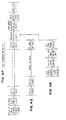
- FIG. 1 represents a background multiprocessing (MP) system containing the described embodiment of the invention.
- the MP illustrated in Figure 1 comprises four central processors CPO through CP3, in which each CP includes an instruction execution (IE) unit and a buffer control unit (BCE).
- Each IE includes the hardware and microcode which issue instructions which require the fetching and storing of operands in main storage (MS).
- the IE begins a fetching or storing operation by issuing a fetch or store command to its cache controls (BCE), which includes a processor store-in-cache (SIC) with its associated processor cache directory (PD) and all processor cache controls which are exclusively used by the associated CP.
- BCE cache controls
- PD processor cache directory
- the CP generally issues a fetch or store command for each doubleword (DW) unit required by an operand.
- the DW is in the PD (as in the case with most processor fetch and store commands), the DW is fetched or stored in the cache in accordance with the command, and the command is completed without any need to go outside of the BCE. Occasionally the required DW is not in the cache, which results in a cache miss. Before the IE fetch or store command can be completed, the DW must be fetched from MS. To do this, the BCE generates a corresponding fetch or store miss command which requests an associated system controller (SC) to obtain from MS a line unit of data having the DW required by the IE. The line unit will be located in MS on a line boundary, but the required DW will be the first DW in the fetched line to be returned to the requesting BCE.
- SC system controller
- each SC is connected to two CPs and to the shared main storage (MS), so that either connected processor can access any shared area in main storage.
- Each SC also connects I/O to the shared main storage.
- Each SC may include the subject matter disclosed in European patent applications 79 105 164 (publication number 12951) and 80 103 081 (publication number 21144).
- the shared main storage comprises of a plurality of BSM controllers BSCO through BSC3 in which each BSC connects to two BSMs 0 and 1.
- the four BSCs 0-3 are each connected to each SC.
- a cross-interrogate (XI) bus connects from each SC to the other SC.
- the XI bus communicates all cross-interrogation (XI) requests and all castout (CO) and invalidate (INV) signals between the SCs to synchronize and coordinate the required castouts, MS fetches, and invalidations in the directories.
- Each SC contains a pair of copy directories.
- Each copy directory contains an image of the contents of a corresponding processor cache directory (PD) in one of the BCEs connected to the respective SC. Both PD and CD are addressed by the same bit positions from the logical address.
- the copy directories handle all cross-interrogation (XI) requests, so that the processor cache directories in the various BCEs will not need to handle the XI interrogation requests and can thereby better service their respective CPs.
- the XI bus connects all SCs and synchronizes all CD searches for conflicts so that XI searching is avoided in the PDs.
- Each of the other CPs 1-3 has an IE identical to the IEO.
- Each IE unit is basically similar to IE units found in conventional microprogrammed processors.
- a doubleword wide bidirectional bus is provided between each BSM in main storage (MS) and each SC port, and from each SC to each associated central processor (CPU) and 1/0 channel controller (EXDC) processor. Both commands and data may be sent on any bus.
- a CPU cannot find a requested doubleword (DW) in its cache
- its buffer control unit (BCE) which controls the CPU cache
- SC system controller
- SC system controller
- the SC will save the request in a command queue and will reissue it at a later time when the required BSM becomes available.
- the SC also sequences the MS commands in an orderly fashion, so that all commands to a particular BSM are issued in first-in/first-out (FIFO) order, except when a cache conflict is found.
- FIFO first-in/first-out
- a real address to physical address transformation is performed by the SC to determine the BSM location of the real address. See European patent application 79 105 164 (EP-A-0 012 951).
- the request is sent to the storage key array to check for a possible access storage protection violation, as well as to the copy directories in all SCs to search for a possible data contention conflict.
- the SC is constantly monitoring the status of main storage, is analyzing the interrogation results of the storage protect key and all cache directories, is examining the updated status of all pending commands currently being held in the SC, and is also looking for any new BCE commands that may be waiting in the BCE to be received by the SC.
- the main storage protect key arrays are located in the system controller as described and claimed in European patent application 80 103 081 (EP-A-0 021 144). It performs all key operations defined by the IBM system/370 architecture. Normally, the storage key is checked in parallel with the issuance of the request to memory and this check does not interfere with actual main storage access time.
- CP changed data resides in the CP SIC and is not available in MS until the data is castout of the SIC by the cache line replacement mechanism whenever cache line space is required for newly requested lines.
- Each SIC has a processor cache directory (PD) which controls its SIC operations.
- each CP's updated lines in its SIC are not stored in MS immediately. Thus, many lines of shareable, unchanged and changed data may be scattered among the SICs. Unchanged SIC lines are available in MS, but changed lines are only available in the SIC in which they reside. Each SIC line is given a shareability designation, which is used by the MP cache management controls to apply appropriate control over the type of shareability of each line while in one or more SICs in the MP.
- any IE requests instructions with the parallel shareability designation of readonly, because instructions are not expected to be changed.
- operand data are generally requested by the IE with the serial shareability designation of exclusive, because they are to be changed, or are likely to be changed.
- the IE shareability designation is provided in Figure 5 on line 24, on which an up signal state indicates an exclusive (EX) designation for the current IE request, while a down signal state indicates a readonly (RO) designation for the current IE request to the BCE in the CP.
- EX exclusive
- RO readonly
- a CP request may be for a doubleword (DW), unit for the CP, it is accessed from a line unit of operand data and/or instructions in its cache.
- Main storage accessing efficiency is greatly improved by having line units of plural DWs (e.g. 16 DWs) accessed as a unit in MS for each cache, and each cache directory is organized to manage its content on a line basis. Therefore, the shareability designation in the cache is done on a line unit and not on a DW unit basis.
- the line shareability designation is checked for each CP DW unit access in the cache and any IE store request causes a cache miss when the shareability designation for the accessed line is RO; but any IE fetch request is immediately accessed. If the line designation is EX, both IE fetch and IE store requests are immediately accessed into the line in the cache.
- any IE initiates an operand or instruction fetch request
- the IE issues a fetch command such as shown in Figure 3A for a doubleword (DW) of data or instructions to its BCE with one of the following two types of sharing control designations:
- the DWs in the line in the cache may immediately be fetched. All CPs can simultaneously access the line in their processor SICs as long as they need only fetch the data in the line. Any CP store request for a DW in a line designated RO causes a cache miss which changes the designation to EX and forces any other CP sharing the line RO to invalidate its copy of the line.
- the DWs in the line may be fetched or stored into by the CP possessing the line exclusively. No other CP can access the line. If another CP must access the line, the CP possessing the line must give up the line to the CP requesting the line which then becomes the only CP possessing the line. If the possessing CP has stored into the line (i.e. changed it) the possessing CP has the latest version of the line; and the line version in MS is not the latest version and should not be accessed. Therefore, the possessing CP must castout a changed line to MS to provide the latest version in MS whenever another CP is to obtain the line, whether or not the possessing CP will continue to possess the line with a readonly designation.
- the present invention has recognized, that a line designation can be changed from exclusive to readonly to enable parallel shareability in spite of IE requests for exclusivity; it has further recognized, that the directory line shareability designations can be used to advantage in the way cache synonyms are handled.
- the current line shareability designations in each SIC in the MP are contained in the processor directory (PD) associated with each SIC in the MP.
- the BCE containing each PD enforces the rules pertaining to the shareability designations in the PD, and generates a cache miss for the current IE request whenever the requested PD class does not contain an entry with the translated request address. A request in a synonym entry will cause a cache miss. Inter-CP communication is required for servicing each cache miss.
- CDs copy directories
- the nomenclature used herein distinguishes the issuing CP (which may be any CPO-CP3 in the MP issuing a storage request command being Xled) from each of the remote CPs (which is the remaining CPs of CPO-CP3 that did not issue the command for which they are being Xled).
- the issuing CP and all of its associated cache entities i.e. its IE, BCE, PD, SIC and CD
- the suffix (I) i.e. IE(I), BCE(I), PD(I), SIC(I) and CD(I).
- Every remote CP and all of its cache entities are identified with the suffix (R), i.e. IE(R), BCE(R), PD(R), SIC(R) and CD(R).
- a cache miss signal occurs if a CP(I) requested DW is not identified in its PD(I), i.e. not in PD(I) or in a synonym entry in PD(I), or is identified with a RO designation when the CP(I) is requesting a storage write access.
- the CP(I) cache controls in its BCE(I) request a fetch of the line containing the requested data, and a cross-interrogation (XI) of the directory CD(I) to check for synonyms and of all other directories CD(R) in the MP to check for conflicts to assure that the requesting SIC(I) will receive the latest version of that line, and invalidate an exclusively obtained line when it is held in any SIC(R).
- the XI operation searches the copy directories CD's of all CP's to determine if any CP cache has the line (i.e. a cache conflict).
- Virtual address bits from the IE logical address are used to address the cache directories; and they only address the principle cache class and they do not address any synonym class in PD or CD. Then each potential synonym class must be searched for the absolute address translated from the CP request in order to detect the existence of any synonym line.
- PD(R) changes the EX bit to RO state and issues a CERO (change entry to readonly) command to its associated CD(R) to do likewise.
- the BCE sets the V (valid) bit to invalidate state in the PD(R), initiates a castout (CO) of the line from the associated SIC, and issues a castout (CO) command to the SC which causes the conflicting entry in the corresponding CD(R) to have the V bit set to invalidate state.
- SI store interrogate
- each CD(R) must be cross-interrogated for the address of the request to determine if its SIC has conflicting data. If a conflict is found in a CD(R) holding the data exclusively or holding it RO when there is an I/O or SVP store or fetch request, the CD(R) communicates with its PD(R) and the line is invalidated if unchanged, or castout and invalidated if changed.
- SVP service processor
- BCE(R) sends an ILE command to the CD(R) controls to invalidate the specified directory line entry in the CD(R).
- BCE(R) transfers the line having the request address from SIC(R) to MS through a line store buffer (LSB) in BCE(R), which causes the CD(R) entry to be invalidated upon the successful completion of the store operation.
- LSB line store buffer
- SC command asking BCE(R) to test the CH bit in PD(R) and make an appropriate command to CD(R), i.e. a CERO or CO command.
- the SC connects between MS and the BCEs and the I/O channels by using 72 line bidirectional busses (64 data/command lines plus 8 ECC lines) to provide a doubleword parallel transfer for both the commands are transmitted.
- CD(I) for a BCE(I) miss command
- Table 2 The different synonym and non-synonym detection conditions in CD(I) for a BCE(I) miss command are represented in the following Table 2, in which the acronym meanings are in parethesis: CMD (Command), LF (Line Fetch), Syno (Synonym), Desig (Designation, # (Number of Copies of the Requested Line), Inval (Invalidation), OP (Operations), CP Acc (Processor Accesses), Princ (Principle), and FTH (fetch request state of the SI bit):
- a BCE(I) miss command for a line fetch causes SC(I) to search CD(I) for synonyms at the same time and in the same CD classes that each CD(R) is searching for conflicts in its principle and synonym locations for the same BCE(I) miss command.
- the BCE(I) miss command bit positions EX and SI shown in Figure 3B exercise control over how SC(I) handles any synonym which might be found in CD(I), as well as the setting of the EX bit in a found synonym entry in CD(I).
- the output compare circuits for CD(I) detect the existence of any synonym in CD(I). An exclusively designated synonym entry is detected by an EX compare (CMPR) signal, and a readonly designated synonym entry is detected by a RO compare signal.
- CMPR EX compare
- an RO synonym is not accessed by a SI (store) request; but since SI requests are always exclusive, duplicate entries are not permitted. That is, only one EX entry can be provided for a given line in all caches in the MP at any one time. Therefore, the line fetch is made to a location in the principle class where its entry is set to exclusive state, and the RO synonym entry is invalidated.
- the RO synonym entry in CD(I), PD(I), SIC(I) remains valid and useable; and therefore the new primary location duplicates a line in the cache, and both must be set to an RO designation.
- the reason why this RO synonym line is not invalidated is that there is no purpose for invalidating it at this time, since it is possible for some other program to get dispatched on CP(I) for which the synonym location may be the principle location. For example, one program may detect a cache location as a synonym, while another program may detect the same location as a principle location, since the principle/synonym relationship is always relative to the requesting address, and they occur for both IE fetch and store interrogate requests.
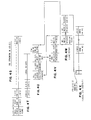
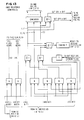
- the pertinent control circuits in each BCE are shown in Figures 5, 13, 14, 15, 16 and 17.
- the pertinent control circuits in each system controller (SC) are shown in Figures 6, 7, 8A, 8B, 9, 10 11 and 12.
- any central processor (CP) must either fetch or store a doubleword (DW) of data
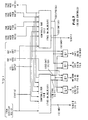
- the instruction execution unit (IE) in the CP issues an IE command to the buffer control unit (BCE) in the CP shown in Figure 5.
- the information in'the IE command is shown in Figure 3A which includes a storage protection key, the logical address of the request, the type of request (i.e. whether it is a fetch request or a store interrogate (SI) request), and whether the data is being requested exclusively (EX) by the CP so that it can store into the data or whether the data is requested non-exclusively (i.e. readonly so that it may be shared among a plurality of processors, none of which is presumed to write into the requested data).
- SI store interrogate
- the SI request indicates that an IE store cache command will subsequently occur when the housekeeping (e.g. translation and/or line fetch) is completed as a result of the SI request.
- the subsequent IE store command contains a store cache signal, after which time the IE provides the data on the bus to be stored in the cache for that address.
- LRU least-recently used algorithm circuit
- An IE command to the BCE contains the logical address (i.e. virtual or real addresss) for a DW of instruction or operand data.
- an activated SI request bit or fetch request bit in the IE command inputs to a BCE priority circuit 37 to formalize the IE request to the BCE(I).
- An output of circuit 37 indicates when the BCE(I) accepts the IE command.
- the logical address is received from the IE command by a BCE address register 31 and is provided to conventional translation and prefixing controls 32, which provide the absolute address, which most of the time may be immediately obtained from a DLAT (dynamic look-aside address translation) array 34. If not in the DLAT, then DAT (dynamic address translation) hardware 33 is invoked to translate the address and place the translation in an entry in DLAT 34. The translated absolute address of the request is put into an absolute address register 36.
- DLAT dynamic look-aside address translation
- the BCE address register 31 outputs six bit positions 19-24 of the logical address as a class address to PD class addressing controls 41 to select a PD class entry in PD 62 containing four set-associative line entries.
- the choice of bits 19-24 selects one of 64 classes in the cache.
- the output of abolute address register 36 is then provided to conventional set-associative comparators in PD 62 to select any line entry in the selected class that matches the absolute address.
- Figure 17 shows this comparator circuitry in detail. If no match is obtained, a no select output is activated which provides a cache miss signal. If a match is obtained, data exists in SIC 63 at a line location associated with the matched entry in PD, and the requested DW is accessed in this line.
- a cache miss If a cache miss occurs, it activates an LRU circuit 42 to choose the least recently used entry (i.e. set A, B, C or D) in the same PD class for receiving the tags for the line to be fetched from MS. If the valid bit is off in the selected line entry, or if the valid bit is on and the CH bit is off in this entry, it is immediately available for the new line. If the valid bit is on and the CH bit is on, then an updated line currently resides in this entry and it must be castout before the new line can be received by the SIC 63.
- the least recently used entry i.e. set A, B, C or D
- a BCE miss command is generated in the BCE and sent to the SC in order to make a line fetch request to MS, and to initiate the XI operations.
- the miss command is shown in Figure 3B and is formed in BCE command/data register 45 which receives the absolute address of the requested data from register 31.
- the BCE command also receives the PD set field from LRU 42, an OP code field from OP encoder 38 which encodes the fetch or store interrogate bit in the IE command, a length field from a DW length circuit 39 which indicates the number of doublewords in a line to be fetched or stored, a SI bit field which indicates whether or not the miss command is a result of a store or fetch command from the IE, and an EX signal field which indicates whether or not the IE requested the data exclusively or readonly.
- the processor ID field is not transmitted by the BCE but is inserted by the SC when it receives the command, in order for the XI operation to identify the processor from which the command was received, since the XI operations use commands from a number of different processors including one or more CPs, an 1/0 processor and a service processor.
- a BCE request trigger 43 is set by an AND circuit 47 which receives a signal from the BCE priority circuit 37 after it accepts the IE command and a miss occurs.
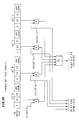
- a PIR priority circuit 101 in the SC determines when the SC accepts a BCE command, and gates it into PIR 103 in the SC.
- a processor identifier (PID) encoder circuit 102 encodes the PID of the processor which had its command accepted by circuit 101, and inserts the PID into the command in PIR 103.
- An XIR register 104 receives the command from PIR 103 during the next machine cycle.
- An XIR priority circuit 110 determines when the command in XIR 104 will be gated into a directory register 121 via a gate 122, from which the command signals initiate an XI operation by being provided to Figure 7 representing the controls in one SC containing CDO and CD2. If another SC exists having CD1 and CD3, it will simultaneously receive these signals from XIR 104 on the XI bus 19 in Figure 1. This initiates a simultaneous search of all copy directories in all SCs (whether the MP has only a single SC or plural SCs).
- the XI search sync lines 111 in bus 19 in Figure 9 connect between plural SCs to synchronize all CD searches in the same machine cycles. The search is for the absolute address of the line currently in each directory register 121.
- an output of circuit 110 sets a local SC busy trigger 112. If any CD finds the searched address, it generates a conflict signal on line 130 for CDO in Figure 8B (or a corresponding line 130 for any other CD).
- Figures 8A, 88 and 8C show SC circuits for generating the CDO conflict signal 130 from a CDO conflict trigger 137.
- CD(I) finds a conflict when a readonly match is detected in a synonym class.
- each CD has an entry for every line found in its corresponding PD, the CD need not have all of the information found in its corresponding PD.
- This embodiment only requires that each CD have the tag information shown in Figure 2B which includes the valid (V) and exclusive (EX) bits and high-order absolute address bits 8-20 for each represented line.
- the tag entries found in each PD line entry are shown in Figure 2A.
- Each PD line entry additionally contains a protect key, a fetch (F) protect bit, and a page change (PG CH) bit.
- An additional tag bit in the PD is the LN CH bit, which hereafter is referred to as the CH bit which indicates whether or not the corresponding line is changed in the associated SIC.
- each IE sends fetch and store requests to its associated BCE.
- Store (SI) requests are always requested exclusively. Instruction fetch requests are requested readonly. Operand fetch requests are requested exclusively. Under special circumstances, the EX tag bit for a required line is set to RO state in spite of an exclusive operand fetch request by the IE. If an operand fetch is requested exclusively by IE(I), and PD(I) finds the EX bit is off (indicating the conflicting line is held readonly), then the access is permitted in SIC(I), and no cache miss results and no XI operation occurs for the fetch request.
- CD(R) finds its EX bit set to EX state, for the Xled fetch exclusive request command, the SC for CD(R) will transmit an ARO command (as shown in Figure 3C) to PD(R).
- the SC command includes the class and set addresses in CD(R) indicating where the conflicting entry was found, and the command contains a castout (CO) command bit, an invalidate (INV) bit, and an alter-to-readonly (ARO) bit the respective line in PD(R).
- the ARO bit is set to make it an ARO command.
- CD(I) finds the EX bit set to EX state for a conflict address, CD(I) sends an EX synonym signal to PD(I) to access the synonym location in SIC(I), as shown in Figures 8A, 9, 12 and 14.
- the command response provided by BCE(R) is shown in Figure 3D, and is determined as indicated in Table 1 herein which shows how the BCE command is dependent on the state of the change (CH) tag bit for the line in PD(R).
- the specific command response is dependent upon the command request type, its PID and EX bit state.
- the BCE(I) miss command execution is suspended and this command is held in the SC command queue (not shown), until BCE(R) responds to the CD(R) command requesting ILE, CO or CERO.
- BCE(R) receives an ARO command and the CH bit is on in PD(R) for the conflicting line, a castout is required from SIC(R), and the castout begins as soon as PD(R) accepts an SC ARO command and finds the CH bit is on for the conflicting line.
- the BCE responds with a castout (CO) command to the SC which sets the V bit off for the entry in CD(R). If CH is off, the line is unchanged and BCE(R) will reset its EX bit to RO state and issue a CERO (change entry to readonly) command to the corresponding CD(R), in order for the CD(R) to set its corresponding EX bit to RO state for the line.
- the CERO command will cause the BCE(I) miss command to be taken from the SC command queue and again XI searched.
- CD(R) In response to the CERO command, CD(R) changes its EX bit to RO state. Then the next iteration of the BCE(I) miss command processing will find a RO state in the CD(R) entry, which will cause an ATRO signal to the SC for CD(I) to set the EX bitfor the line to RO state.
- the hardware for this operation is shown in Figures 5, 7, 8A, 8B and 8C.
- the issuing CD(I) Whenever the ATRO signal is received by the issuing CD(I), it generates a ROD (readonly designation) signal which it sends to its corresponding PD(I) to reset its EX bit for that line to the RO state, in order to indicate that the line will thereafter be held in RO state in the issuing processor SIC(I) as well as being in the RO state in each SIC(R) finding the conflict.
- ROD readonly designation
- All storage commands are handled through several phases of sequencing control in the SC; and at any instant of time, several different phases of different storage commands may be processed concurrently in the SC.
- the normal sequencing of BCE fetch and store commands includes the following described operations.
- the command is also having its PSW storage key checked in the SC for possible key violations, as disclosed and claimed in prior cited application EP 80 103 081 (EP-A-0 021 144).
- the SC checks for the availability of the BSM and its controller required by the address in the command, as disclosed and claimed in prior cited application EP 79 105 164 (EP-A-0 012 951 If the BSM is not busy, the MS command is sent to the BSM immediately. On the other hand, if the BSM is found to be busy and/or a conflict is found, the command is saved in the SC command queue and the queue array, to be reissued when the BSM becomes available and/or the conflict is resolved. Each time an XI operation iteration is completed, the status for the MS command is again updated in the command queue.
- the BSC may or may not start the storage access immediately (depending on whether there is a previous storage access in progress).
- the BSC will signal the SC when a data ready condition exists.
- the SC Because of the long memory access time relative to the CP cycle time, by the time the BSC signals data ready, the SC has normally completed all status checking related to the MS command. If directory conflicts or key violations are detected, the MS data transfer phase of the operation is cancelled, and may subsequently be reissued after the conflicting conditions are resolved. However, with most MS commands, no conflict or violation is detected; therefore, the data transfer takes place immediately after the SC has checked that both MS and CPU data transfer paths are not busy.
- BCE miss command requires a line fetch from MS to SIC(I).
- a cache miss may also require a line castout from SIC(I) in the issuing processor to make room for the required line fetch if the LRU selected location is occupied by a valid changed line. If the XI operation flinds the requested line was updated in any SIC(R), the line must be cast out of SIC(R) before it can be line fetched by SIC(I).
- the three phases of control described above namely, BCE command processing, MS access control, and the data transfer, are all independently handled in the SC.
- the control of each phase can begin processing a new command in that phase as soon as the phase has finished processing the previous command. Therefore, several different commands can be processed concurrently in the SC by its different phase controls.
- Figures 4A through 4F illustrate timing sequences for a BCE miss request having an XI conflict with the CH bit on and requiring two line castouts from SIC(I) and SIC(R) prior to the line fetch.
- Figures 4H through 4N illustrate timing sequences for a BCE miss request requiring only a castout by the issuing processor SIC(I) prior to the line fetch.
- Figure 4A illustrates a cache miss followed by the castout of the sixteen DWs of a valid changed line in SIC(I) to its LSB(I) to make room in SIC(I) for a requested line fetch.
- the castout uses a line store buffer (LSB) 51 shown in Figure 5 in order to free up SIC(I) before the castout line in LSB is stored into MS, which otherwise would delay the line fetch, so that the line may be made available to CP(I) much earlier than if its DWs were directly transferred from SIC to MS.
- LSB line store buffer
- the SC receives the BCE miss command in its PIR(I) 103 (the circuits are shown in Figure 6) two cycles after the BCE received its request from IE(I).
- the command is received by XIR(I) 104.
- XIR priority is given by circuit 110 on the following cycles, the command is transferred by gate 122 into directory register 121 in the local SC(I), and simultaneously via the XI bus to gate 123 into directory register 121 in each remote SC(R), if any.
- Figure 16 shows a detailed circuit for testing the state of the CH bit in any selected PD output register.
- BCE(R) sends a castout (CO) command from its command register 45 in Figure 5 to SC PIR 103.
- PD(R) is updated by BCE(R) invalidating the entry, and simultaneously issues a CO command to SC(R). Then the SC loads its CO register 211 in Figure 8C, and CD(R) is updated by its SC invalidating the entry. Then during the fourth cycle in Figure 4D the castout begins by moving DWO of the addressed line in SIC(R) to LSB(R), etc. until all sixteen DWs of the line are received in the LSB(R), after which in Figure 4E the LSB(R) provides the updated line to MS from which it is available for a line fetch to the requesting SIC(I) in Figure 4G since the XI operations in Figure 4C are most likely completed by this time.
- the line castout from SIC(R) to LSB(R) may overlap the line castout from SIC(I) to LSB(I) if both castouts are required.
- the requested line fetch from MS shown in Figure 4G may begin as soon as the castout of the updated line is completed to MS, which is shown in Figure 4E, i.e. LSB(R) to MS of the sixteen DWs.
- the line fetch begins with the requested DW(N) which is the DW at address N requested by the IE command which caused the cache miss.
- the line fetch of the 16 DWs may wrap around to the beginning of the line before it ends with the sixteenth DW (N-1) into SIC(I).
- the castout transfer from any LSB to MS is controlled by the absolute address of the line in CO address register 211 in Figure 8C, which is received in the SC from the command currently in its directory register 121 in Figure 6.
- the SC signals a CO complete status to BCE(R) which sets its CO complete trigger in Figure 14 if all conditions indicate the CO is successful and the line is available in MS.
- the output of the CO complete trigger is provided to a reset input in the CO address register 211 in Figure 8C in order to make it available for a next castout transfer operation to MS.
- Figures 4H-4N show an example of a remote conflict having the CH bit off (indicating the line was not changed) as shown in the third cycle in Figure 4L (corresponding to the third cycle in Figure 4D). Then BCE(R) sends a CERO command from Figure 5 to Figure 6.
- Figures 4H-4N show a line fetch after a one line castout.
- Figure 4H is identical to Figure 4A;
- Figure 4J is identical to Figure 4B and
- Figure 4K is identical to Figure 4C.
- Figure 4L differs from Figure 4D only in their fourth cycle, in which in Figure 4L a CERO command is issued by the BCE(R) because the CH bit was off for the line being addressed, which negates any castout from SIC(R).
- CD(R) has its EX bit updated to RO state by the CERO command, and Figure 4K is reentered to search all CDs to verify that no conflict now exists.
- the SIC(I) castout operation in Figures 4H and 4M is controlled the same as previously described for Figures 4A and 4F to make room for the line fetch. Likewise the SIC(I) castout operation overlaps the cross-interrogation operation in Figures 4K and 4L, and the line fetch command for MS has been provided and is waiting in the SC queue of MS requests. As soon as the SIC(I) castout is completed to LSB(I), and the final XI pass through Figure 4K finds no conflict exists, the line fetch can begin from MS to SIC(I) as shown in Figure 4N.
- Figures 4C and 4K illustrate the timing for cross-interrogate operations when the MP system is operating in 4KB page mode, i.e. translation page tables address 4KB page units.
- the MP may operate in either 4KB or 2KB page mode in which its page tables may access 4KB units or 2KB units, respectively.
- the significance of the page mode to the subject invention is that virtual address bits used in the cache directory class address differ between the 4KB and 2KB page modes and affect the number of synonym class addresses which must be XI searched in each 32KB SIC.
- For 4KB page mode only bit 19 in the class address is a virtual address bit resulting in two class addresses to be searched.
- bits 19 and 20 in the class address are virtual address bits resulting in four class addresses to be searched.
- virtual bits are taken from the logical address before its translation, in order to speed up the cache access time for a requesting CP to a large cache.
- An adverse result of using virtual bits is that the number of virtual address bits determines the number of synonym classes (as a power of 2) which must be searched in the directory; and the greater the number of virtual bits, the more synonym searching must be done in the directories.
- Synonym searching is done in all copy directories (CD).
- a separate machine cycle is used simultaneously in all CDs in the MP for searching each original and synonym class of the absolute address in the current BCE miss command.
- two cycles are needed to search all CDs for the original and the synonym class as shown in Figures 4C and 4K.
- 2KB page mode four cycles are needed to search all CDs for the original and three synonym classes.
- the first cycle searches the original class determined by the absolute address virtual bit 19 in the transmitted XI command.
- bit 19 is inverted in the class address to select the only synonym class.
- each synonym class is obtained by a different one of four permutations of the value of virtual bits 19 and 20 to search the original and the three synonym classes in all CDs.
- This searching performs true synonym searching in CD(I) and conflict synonym searching in each CD(R). If a synonym match is obtained in CD(I) and the CD(I) entry is exclusive, the synonym address is transmitted by the SC to BCE(I), which then accesses the request in that synonym address in its SIC(I) and simultaneously releases the BCE miss command, cancels the MS request, and treats the situation as if no miss had occurred.
- An EX compare is signalled on line 161 in Figures 8C and 8A for CD(I), and a RO compare is signalled on line 162 for CD(I).
- a RO compare signal on line 162 is handled as a conflict in CD(I) and CD(R), via OR circuit 163 in Figure 8B, and it generates an MP conflict signal in conflict trigger 137 in Figure 8C.
- Figures 10, 11 and 12 illustrate in detail the CDO synonym circuits shown in block form in Figure 8C which control the synonym searching for 2KB or 4KB page mode.
- a start XI signal from the XIR priority circuit in Figure 6 initiates the XI search cycle generation in Figure 11.
- the first search cycle for all CDs is of the original class address provided in the current BCE(I) miss command from the directory register 121 in Figure 6, which occurs during the cycle of operation for trigger/latch T1 in Figure 11. If the 2KB mode signal is active to Figure 11, 2KB mode synonym searching is performed during the following cycles by T2, T3 and T4. If the 2KB mode signal is inactive to Figure 11, then 4KB mode synonym searching is performed and only the additional cycle by T2 is used for searching, which involves two less searching cycles than for the 2KB page mode.
- the flip 19 and increment 19, 20 outputs from Figure 11 are provided to Figure 10 to control the permutations of bits 19 and 20 to obtain the synonym CD class addresses required for the respective CD search cycles. All four line entries in the four sets in each selected CD class are searched.
- the synonym capture circuit in Figure 12 receives the current class address bits 19 and 20 from Figure 10 and also receives the associated CD conflict signal on line 130 from Figure 8B to lock the current state of class address bits 19 and 20 in syno 19 and syno 20 triggers 301 and 302, which provides their outputs to the PD class addressing control circuits in Figure 14. The remaining bits 21-24 in the class address remain as specified in the current command being searched.
- Trigger 320 is set by a signal from a CD(I) exclusive synonym trigger 142 in Figure 8A, and trigger 142 is set only when the issuing BCE command in the directory register 45 has a PID which identifies CP(0) as the processor which issued the request which caused the current BCE miss being searched by all CDs.
- trigger 142 in Figure 8A can only be set when the issuing command's PID activates line 144 to an AND gate 143 when it is actuated for an exclusive synonym detected by that command.
- line 321 conditions an AND gate 322 which also is conditioned by an output from a status decoder 323 when it indicates an error-free status is being provided from the SC status encoder in Figure 9.
- line 321 will not be activated to any PD(R), because the PID for each remote CP will not then exist in the current BCE miss command being processed in every SC.
- an AND gate 136 in Figure 8B determines that the EX tag bit for the requested line, whether in the principle or a synonym class, will be set according to the rules given in Table 1 herein. If the RO state is to exist, gate 136 provides a CD(I) ROD signal on line 137 to the ROD trigger 401 in Figure 15, which sets the EX bit to RO state in the particular PD input register for the set chosen by the PD LRU circuit associated with the issuing CP(I). The states of the V bit, CH bit and absolute address bits 6-20 for the line fetch entry into PD(I) are also controlled in Figure 15.
- a conflict signal is provided whenever any remote processor CD(R) detects any principle or synonym address except for an RO synonym found for a RO processor request, or whenever the issuing processor CD(I) detects a RO synonym address in response to an SI request from the issuing processor.
- Remote processor CD(R) conflicts are explained using Table 1 and the previously discussed examples in Figures 4A-G and 4H-N.
- Issuing processor CD(I) conflicts are explained using Table 2 and the examples in Figures 4P-R and 4S-X.
- the respective rows represent the different combinations which can exist for: the different processor request types in an XI command, and the RO and EX types for a line address found in a remote processor CD(R).
- the particular cases of a RO processor fetch request (or an SVP or channel processor fetch request) finding a RO line address in CD(R) is not a true conflict, because all processors can share such a RO line for RO fetch requests without any directory changes.
- These non-conflict situations are represented by the 1st, 4th and 10th rows in Table 1. All of the other rows in Table 1 represent conflict situations, because they require a directory change, which is done by an SC command from any remote CD(R) that finds a conflict to its respective PD(R), which is shown for all rows in Table 1 other than the 5th row.
- the respective rows represent the different combinations which can exist for: the different processor request types represented in a BCE miss command (i.e. RO fetch, EX fetch or EX SI), and the synonym type (i.e. RO synonym or EX synonym) found in CD(I).
- a BCE miss command i.e. RO fetch, EX fetch or EX SI
- the synonym type i.e. RO synonym or EX synonym found in CD(I).
- Only the 5th row in Table 2 represents a true conflict situation, because it is the only case requiring any special directory change to an existing entry, which is done by an ILE command from CD(I) to PD(I) to change these directories.
- the remote CP(R) conflict cases in Table 1 are detected in Figure 8A by AND gates 166, 167, 168 and 169. All conflicts are signalled by the output of an OR circuit 164 in Figure 8A which receives the outputs of gates 166 through 169.
- the issuing processor CP(I) conflict case in Table 2 is also detected by AND gate 169.
- an EX synonym is detected by an EX compare (EX CMPR) signal 161 from comparator 171 in Figure 8C, and an RO synonym is detected by an RO compare (RO CMPR) signal 162 from comparator 171.
- EX CMPR EX compare
- RO CMPR RO compare
- Gate 167 detects a RO synonym found for a SVP or channel store request.
- Gate 168 detects an EX synonym found for any remote CP(R) request (but not for a CP(I) request).
- Gate 169 detects a RO synonym found for a SI request from any remote CP(R) or issuing processor CP(I).
- a detected conflict indicates a synonym is found in CD(I), although most synonyms are not detected as conflicts.
- the synonym capture circuit in Figure 12 detects all synonyms and reports each of their class locations to PD(I).
- Detected EX synonyms are handled differently from detected RO synonyms for the following reason: a statistical determination finds that system performance is improved if synonym detection is used (1) to eliminate the synonym and to copy its data into the principle location, rather than (2) accessing the requested data in the synonym location in SIC(I). It has been statistically determined that it is most likely that more requests will follow to a line found at a synonym location, and that relocating that line in the principle class will avoid generating cache misses (required for accessing the line in the synonym location), thereby eliminating such subsequent cache misses with their significant cross-interrogation and synonym checking overhead. However, this cannot be done for an EX entry locked during a checkpoint interval. (Checkpointing is defined in U.S.A. patent 3 736 566.) An EX entry may be locked, and then it cannot be invalidated or castout during a checkpoint interval. However, an RO entry is never locked during a checkpoint interval and therefore it can be then invalidated and castout, if required.
- a SC command specifies the EX synonym location to PD(I), which accesses the data in SIC(I), and the line fetch command to main storage is then cancelled, so that no MS line fetch is made.
- an EX synonym is accessed in SIC(I) instead of moving it to the principle class, because a processor deadlock may result if an attempt is made to move a locked line from the synonym class to the principle class in the cache.
- the deadlock occurs because a changed EX location cannot be castout while its line is locked during a checkpoint interval, and the checkpoint interval cannot be completed by the I-unit until it gets the data requested from the line fetch which cannot be obtained until after the castout (which cannot be done) is completed.
- Figures 4P through 4R illustrate a timing sequence example for a BCE miss command which finds an EX synonym in CD(I).
- Figures 4S through 4X illustrate a timing sequence example in which a BCE miss command finds an RO synonym in CD(I).
- the first cycle for the EX synonym example in Figure 4P represents a miss detection in PD(I) due to a CP(I) fetch request and the issuance of the BCE miss command.
- the next cycle illustrates the castout of the first DW of any valid changed line selected by the LRU for replacement in the principle class of the current request. This castout occurs into the line store buffer (LSB) in the same manner as described for Figures 4A or 4H, and begins before any synonym can be detected. If an EX synonym is subsequently detected, it will squelch the castout (but an RO synonym will not squelch the castout).
- LSB line store buffer
- Figure 4Q begins in the manner previously described for Figure 4B in which the SC PIR(I) is loaded, then the XIR(I) is loaded while the local SC, i.e. SC(I), remains busy handling the BCE(I) miss command.
- the directory registers 121 (D regs) in all SC's are loaded, and all CD's are searched in their principle class.
- the CDs are searched in their synonym class (for 4K page mode).
- all SC's wait to determine if any conflict has been detected in CD(I) or in any CD(R) by a remote conflict signal on the XI bus as a result of such searches.
- the fourth cycle in Figure 4R is entered.
- the EX synonym signal detected by trigger 142 in Figure 8A causes a BCE(I) synonym release signal on line 321 to reset the LSB(I) as shown in the reset LSB(I) cycle in Figure 4P which prevents any subsequent transfer of the castout into LSB(I), cancels the corresponding line fetch command to MS, and thereby ends execution of the BCE miss command.
- the EX synonym signal in Figure 8A sets the BCE(I) synonym release trigger 320 in Figure 9 which generates a command cancel signal to the main storage controls in the SC to cancel the line fetch command to main storage initiated by this BCE miss command.
- the PD(I) is caused to select its EX synonym entry after the BCE(I) synonym release signal is received on line 321 in Figure 14, the CD(I) synonym address bits 19 and 20 are received from Figure 12, and the CD(I) class address bits 21-24 are contained in'the current CD(I) command to the BCE(I), PD(I) controls SIC(I) to access the doubleword being requested, which is provided to IE(I) as the last cycle shown in Figure 4P.
- the IE request is now satisfied.
- the RO synonym example in Figure 4S also begins with a BCE miss command resulting from a processor SI request.
- the LRU selects in the principle class in PD(I) one entry (among the four sets A-D) for replacement which is not locked and is therefore immediately available for replacement.
- LSB(I) receives a castout of any valid and changed line in the LRU selected replacement location. In this case, LSB(I) is not reset, because an RO synonym is detected, EX synonym trigger 142 is not set when an RO synonym is detected.
- the BCE miss command is received by PIR(I) in SC(I) during the first cycle in Figure 4T which begins similarly to the operation described for Figure 4Q. Also, Figure 4U begins the synonym and XI searching similarly to that described for Figure 4R. During the third cycle in Figure 4U, a conflict may or may not be detected for an RO synonym.
- the fourth cycle in Figure 4U is reached if no synonym is found or if a RO synonym is found for a processor fetch request (but not for a SI request). Then no command is generated and the EX synonym trigger 142 is not set and indicates no EX synonym was found. Then the line fetch command to main storage remains active, and it begins in Figure 4W with the requested DW(N) which is provided simultaneously both to IE(I) and to SIC(I) during the first cycle in Figure 4W. The completion of the castout from the LSB to MS begins in Figure 4X as soon as the line fetch in Figure 4W is completed.
- the first cycle in the sequence shown in Figure 4V is entered.
- the V bit in this RO synonym entry in PD(I) is set to invalid state.
- the third cycle in Figure 4V represents the issuance of an ILE command by BCE(I) to SC(I) to invalidate the corresponding RO synonym line entry found in CD(I), which ends its conflict state.
- the beginning of the sequence shown in Figure 4U is reentered, after which all of the CDs in the system are again searched, because now no conflict is found in CD(I) since the RO synonym entry which previously caused the conflict is now invalid and does not now cause any conflict signal. Therefore, the fourth cycle in Figure 4U is entered since no conflict is found, and then the line fetch in Figure 4W is initiated. Whenever the line fetch is completed, the castout line in the LSB(I) is transferred to MS as shown in Figure 4X.
- a "conflict" in this detailed description is a compare-equal output from any XI compare operation for any CD that results in a SC command to the corresponding BCE for changing an existing entry in the corresponding PD, whether for a remote or issuing CP.
- a RO compare for a RO processor request is not a conflict, and for the issuing processor the only conflict is a RO compare for a SI request.
- CPU(I) issues to its PD(I) a fetch address W requesting the data exclusively.
- the SC(I) having the copy directory, initiates a search of all copy directories (CDO, CD2 in SCO and CD1, CD3 in SC1) in the MP to determine if any cache in the MP has the line containing address W. Finding no match in any CD, SC(I) accesses MS for the line containing address W, which is sent through SC(I) to the cache for PD(I), with the first sent data item being the requested item at address W.
- Both directories CD(I) and PD(I) are updated to show that the line at address W is held exclusively in the PC(I) cache.
- CP(I) issues to its PD(I) a fetch address X requesting the data exclusively.
- the SC(I) having CD(I) obtains a search of all directories CDO-CD3 for the line having address X.
- Remote CD(R) finds its SIC holds the line exclusively.
- CD(R) sends a SC command (ARO) to PD(R) to test its change (CH) bit for the line having address X.
- the PD(R) test finds the line is held exclusive and is changed.
- PD(R) castsout (CO) that line from its cache to MS at address X, which causes both PD(R) and CD(R) to invalidate the line containing address X.
- CO castsout
- the SC(I) having CD(I) of the issuing CP(I) fetches the line from MS at address X and sends it to the cache for CP(I).
- directories PD(I) and the CI(I) mark the line containing address X as valid, unchanged, and held exclusively in the CP(I) cache.
- CP(I) issues to its PD(I) a fetch address Y requesting the data exclusively.
- the SC(I) having the copy directory, CD(I) initiates a search of all copy directories CDO-CD3 for the line containing address Y. A line address is found in CD(R) which matches the requested line address and it is held exclusively in CD(R). Then the SC having CD(R) sends a command to its corresponding PD(R) to test the line containing address Y. PD(R) then tests the state of address Y and finds that although it is held exclusive, it is not changed. In response, PD(R) does not release the line but updates its entry for the line by resetting its exclusive bit to readonly state.
- PD(R) sends a CERO command to its corresponding CD(R) to change the line entry for address Y to readonly state.
- the SC having CD(R) sends an ATRO (alter to readonly) signal to the SC having CD(I) to change its exclusive tag for the requested line to readonly state.
- the requested data is fetched in MS at address Y and sent to the cache for PD(I) as the first item of the line, as the line is sent in its entirety from MS to the cache for PD(I).
- the SC fetching the line signals PD(I) to hold the line readonly.
- CP(I) issues to its PD(I) a fetch address Z requesting the data exclusively.
- SC(I) initiates a search for the line having address Z in all directories, CDO-CD3.
- a match is found in CD(R) for a line that is held readonly.
- the SC having CD(R) sends an ATRO signal to the SC having CD(I) to change its exclusive tag for the requested line to readonly state.
- the requested line is fetched in MS and sent to the cache for PD(I), beginning with the item of data at address Z.
- a special signal in the SC having CD(I) is sent to PD(I) to tag the line containing address Z is being held readonly.
- a second embodiment of the invention is shown in Figure 18. It implements the synonym processing entirely with the processor directory (PD) without using any copy directory (CD).
- This second embodiment includes the miss detection means shown in Figure 17, which signals the additional searching means 512 upon a cache miss to search the PD 510 for any potential synonym class in the manner described herein for searching the synonym classes in the CD by permitting the translatable bits in the class address.
- Controls 512 include from Figure 8C the synonym search alter circuits 212, the synonym capture circuits 213, and directory addressing circuits 211 which in Figure 18 will operate only in relation to the PD address register in Figure 14 to control the sequential selection of the synonym classes in PD510.
- the synonym comparisons are done in the PD address compare circuits in Figure 17, rather than in the XI compare circuit 171 with the CD in Figure 8C, which are conventional directory comparison circuits. Any synonym location detected during such synonym search is either accessed by the processor from the synonym location or is copied into the primary location in the same manner as described for the previously described first embodiment.
- This second embodiment is not the preferred embodiment for an MP because it results in a degradation in processor performance due to extending the PD(I) operations and search time to include the sequential searching of each synonym class.
- Such single directory embodiment with each central processor in an MP reduces performance due to the additional interference of cross-interrogation. (The CD was provided to relieve the PD of the XI interference in the preferred first embodiment).
Claims (7)
Applications Claiming Priority (4)
| Application Number | Priority Date | Filing Date | Title |
|---|---|---|---|
| US06/205,486 US4400770A (en) | 1980-11-10 | 1980-11-10 | Cache synonym detection and handling means |
| US205486 | 1980-11-10 | ||
| US205500 | 1980-11-10 | ||
| US06/205,500 US4394731A (en) | 1980-11-10 | 1980-11-10 | Cache storage line shareability control for a multiprocessor system |
Related Child Applications (1)
| Application Number | Title | Priority Date | Filing Date |
|---|---|---|---|
| EP86112937.7 Division-Into | 1986-09-19 |
Publications (3)
| Publication Number | Publication Date |
|---|---|
| EP0051745A2 EP0051745A2 (de) | 1982-05-19 |
| EP0051745A3 EP0051745A3 (en) | 1984-07-18 |
| EP0051745B1 true EP0051745B1 (de) | 1988-01-27 |
Family
ID=26900469
Family Applications (2)
| Application Number | Title | Priority Date | Filing Date |
|---|---|---|---|
| EP81107928A Expired EP0051745B1 (de) | 1980-11-10 | 1981-10-05 | Pufferspeicherhierarchie für ein Multiprozessorsystem |
| EP86112937A Expired - Lifetime EP0212678B1 (de) | 1980-11-10 | 1981-10-05 | Anordnung zur Erkennung und Verarbeitung von Synonymen in Cache-Speichern |
Family Applications After (1)
| Application Number | Title | Priority Date | Filing Date |
|---|---|---|---|
| EP86112937A Expired - Lifetime EP0212678B1 (de) | 1980-11-10 | 1981-10-05 | Anordnung zur Erkennung und Verarbeitung von Synonymen in Cache-Speichern |
Country Status (2)
| Country | Link |
|---|---|
| EP (2) | EP0051745B1 (de) |
| DE (2) | DE3177181D1 (de) |
Families Citing this family (13)
| Publication number | Priority date | Publication date | Assignee | Title |
|---|---|---|---|---|
| DE3177181D1 (de) | 1980-11-10 | 1990-06-21 | Ibm | Anordnung zur erkennung und verarbeitung von synonymen in cache-speichern. |
| US4484267A (en) * | 1981-12-30 | 1984-11-20 | International Business Machines Corporation | Cache sharing control in a multiprocessor |
| US4463420A (en) * | 1982-02-23 | 1984-07-31 | International Business Machines Corporation | Multiprocessor cache replacement under task control |
| US4503497A (en) * | 1982-05-27 | 1985-03-05 | International Business Machines Corporation | System for independent cache-to-cache transfer |
| US4695951A (en) * | 1983-07-07 | 1987-09-22 | Honeywell Bull Inc. | Computer hierarchy control |
| US4612612A (en) * | 1983-08-30 | 1986-09-16 | Amdahl Corporation | Virtually addressed cache |
| US4785398A (en) * | 1985-12-19 | 1988-11-15 | Honeywell Bull Inc. | Virtual cache system using page level number generating CAM to access other memories for processing requests relating to a page |
| US4797814A (en) * | 1986-05-01 | 1989-01-10 | International Business Machines Corporation | Variable address mode cache |
| KR920001282B1 (ko) * | 1987-10-02 | 1992-02-10 | 가부시키가이샤 히타치세이사쿠쇼 | 버퍼메모리 제어장치 |
| US5175837A (en) * | 1989-02-03 | 1992-12-29 | Digital Equipment Corporation | Synchronizing and processing of memory access operations in multiprocessor systems using a directory of lock bits |
| US5210848A (en) * | 1989-02-22 | 1993-05-11 | International Business Machines Corporation | Multi-processor caches with large granularity exclusivity locking |
| EP0384102A3 (de) * | 1989-02-22 | 1992-04-29 | International Business Machines Corporation | Mehrprozessor-Cachespeicher mit auf grober Granularität beruhender exklusiver Reservierung |
| JPH035851A (ja) * | 1989-06-01 | 1991-01-11 | Fujitsu Ltd | バッファ記憶装置 |
Family Cites Families (11)
| Publication number | Priority date | Publication date | Assignee | Title |
|---|---|---|---|---|
| US3736566A (en) | 1971-08-18 | 1973-05-29 | Ibm | Central processing unit with hardware controlled checkpoint and retry facilities |
| US3735360A (en) * | 1971-08-25 | 1973-05-22 | Ibm | High speed buffer operation in a multi-processing system |
| US3771137A (en) * | 1971-09-10 | 1973-11-06 | Ibm | Memory control in a multipurpose system utilizing a broadcast |
| US3723976A (en) * | 1972-01-20 | 1973-03-27 | Ibm | Memory system with logical and real addressing |
| FR2344094A1 (fr) * | 1976-03-10 | 1977-10-07 | Cii | Systeme de gestion coherente des echanges entre deux niveaux contigus d'une hierarchie de memoires |
| US4136385A (en) * | 1977-03-24 | 1979-01-23 | International Business Machines Corporation | Synonym control means for multiple virtual storage systems |
| US4136386A (en) | 1977-10-06 | 1979-01-23 | International Business Machines Corporation | Backing store access coordination in a multi-processor system |
| DE2947115A1 (de) * | 1978-12-11 | 1980-06-26 | Honeywell Inf Systems | Loeschanordnung fuer einen cache- speicher eines prozessors in einem multiprozessorsystem |
| US4293910A (en) | 1979-07-02 | 1981-10-06 | International Business Machines Corporation | Reconfigurable key-in-storage means for protecting interleaved main storage |
| US4332010A (en) * | 1980-03-17 | 1982-05-25 | International Business Machines Corporation | Cache synonym detection and handling mechanism |
| DE3177181D1 (de) | 1980-11-10 | 1990-06-21 | Ibm | Anordnung zur erkennung und verarbeitung von synonymen in cache-speichern. |
-
1981
- 1981-10-05 DE DE8686112937T patent/DE3177181D1/de not_active Expired - Fee Related
- 1981-10-05 DE DE8181107928T patent/DE3176632D1/de not_active Expired
- 1981-10-05 EP EP81107928A patent/EP0051745B1/de not_active Expired
- 1981-10-05 EP EP86112937A patent/EP0212678B1/de not_active Expired - Lifetime
Also Published As
| Publication number | Publication date |
|---|---|
| EP0051745A2 (de) | 1982-05-19 |
| DE3177181D1 (de) | 1990-06-21 |
| EP0212678A2 (de) | 1987-03-04 |
| EP0212678A3 (en) | 1987-08-12 |
| EP0212678B1 (de) | 1990-05-16 |
| EP0051745A3 (en) | 1984-07-18 |
| DE3176632D1 (en) | 1988-03-03 |
Similar Documents
| Publication | Publication Date | Title |
|---|---|---|
| US4400770A (en) | Cache synonym detection and handling means | |
| US4394731A (en) | Cache storage line shareability control for a multiprocessor system | |
| EP0061570B1 (de) | Schreib-in-Pufferspeicher Mehrprozessoranordnung mit Prüfpunkt-Eigenschaft | |
| EP0434250B1 (de) | Einrichtung und Verfahren zum Vermindern von Störungen in zweistufigen Cache-Speichern | |
| JP2566701B2 (ja) | 共有キャッシュ内のデータ・ユニットに対する所有権の変更制御装置 | |
| EP0049387B1 (de) | Mehrprozessor-System mit einer "Cache"-Speichereinheit | |
| US5091846A (en) | Cache providing caching/non-caching write-through and copyback modes for virtual addresses and including bus snooping to maintain coherency | |
| US5197139A (en) | Cache management for multi-processor systems utilizing bulk cross-invalidate | |
| EP0258559B1 (de) | Cachespeicherkohärenzsteuerung mit einem Speicher, der ein laufendes Lesen anzeigt | |
| US4884197A (en) | Method and apparatus for addressing a cache memory | |
| US5097409A (en) | Multi-processor system with cache memories | |
| US5696937A (en) | Cache controller utilizing a state machine for controlling invalidations in a network with dual system busses | |
| EP0347040B1 (de) | Datenspeicheranordnung | |
| US6625698B2 (en) | Method and apparatus for controlling memory storage locks based on cache line ownership | |
| US5845324A (en) | Dual bus network cache controller system having rapid invalidation cycles and reduced latency for cache access | |
| US20030023814A1 (en) | Method and system for detecting and resolving virtual address synonyms in a two-level cache hierarchy | |
| JPH11506852A (ja) | 多数のバスマスタと共用レベル2キャッシュとを備える多レベルキャッシュシステムでのキャッシュスヌーピングオーバーヘッドの低減 | |
| EP0139407B1 (de) | Datenauswahlübereinstimmung | |
| EP0051745B1 (de) | Pufferspeicherhierarchie für ein Multiprozessorsystem | |
| US5269009A (en) | Processor system with improved memory transfer means | |
| US5737756A (en) | Dual bus computer network using dual busses with dual spy modules enabling clearing of invalidation queue for processor with store through cache while providing retry cycles for incomplete accesses to invalidation queue | |
| JP2788836B2 (ja) | ディジタルコンピュータシステム | |
| EP1725938A1 (de) | System und verfahren zum abbrechen einer rückschreiboperation während einer gleichzeitigen snoop-push- oder snoop-kill-operation in rückschreib-cache-speichern | |
| JPH07152647A (ja) | 共有メモリマルチプロセッサ | |
| EP0732656B1 (de) | Anordnung von Cachespeicherverwaltungseinheiten |
Legal Events
| Date | Code | Title | Description |
|---|---|---|---|
| PUAI | Public reference made under article 153(3) epc to a published international application that has entered the european phase |
Free format text: ORIGINAL CODE: 0009012 |
|
| 17P | Request for examination filed |
Effective date: 19811005 |
|
| AK | Designated contracting states |
Designated state(s): DE FR GB IT |
|
| PUAL | Search report despatched |
Free format text: ORIGINAL CODE: 0009013 |
|
| AK | Designated contracting states |
Designated state(s): DE FR GB IT |
|
| GRAA | (expected) grant |
Free format text: ORIGINAL CODE: 0009210 |
|
| AK | Designated contracting states |
Kind code of ref document: B1 Designated state(s): DE FR GB IT |
|
| REF | Corresponds to: |
Ref document number: 3176632 Country of ref document: DE Date of ref document: 19880303 |
|
| ET | Fr: translation filed | ||
| R20 | Corrections of a patent specification |
Effective date: 19880215 |
|
| ITF | It: translation for a ep patent filed |
Owner name: IBM - DR. ALFREDO BRAVI |
|
| PLBE | No opposition filed within time limit |
Free format text: ORIGINAL CODE: 0009261 |
|
| STAA | Information on the status of an ep patent application or granted ep patent |
Free format text: STATUS: NO OPPOSITION FILED WITHIN TIME LIMIT |
|
| 26N | No opposition filed | ||
| PGFP | Annual fee paid to national office [announced via postgrant information from national office to epo] |
Ref country code: FR Payment date: 19900926 Year of fee payment: 10 |
|
| PGFP | Annual fee paid to national office [announced via postgrant information from national office to epo] |
Ref country code: DE Payment date: 19901027 Year of fee payment: 10 |
|
| ITTA | It: last paid annual fee | ||
| PGFP | Annual fee paid to national office [announced via postgrant information from national office to epo] |
Ref country code: GB Payment date: 19910923 Year of fee payment: 11 |
|
| PG25 | Lapsed in a contracting state [announced via postgrant information from national office to epo] |
Ref country code: FR Effective date: 19920630 |
|
| PG25 | Lapsed in a contracting state [announced via postgrant information from national office to epo] |
Ref country code: DE Effective date: 19920701 |
|
| REG | Reference to a national code |
Ref country code: FR Ref legal event code: ST |
|
| PG25 | Lapsed in a contracting state [announced via postgrant information from national office to epo] |
Ref country code: GB Effective date: 19921005 |
|
| GBPC | Gb: european patent ceased through non-payment of renewal fee |
Effective date: 19921005 |