EP0051291B1 - Document filing system - Google Patents
Document filing system Download PDFInfo
- Publication number
- EP0051291B1 EP0051291B1 EP81109301A EP81109301A EP0051291B1 EP 0051291 B1 EP0051291 B1 EP 0051291B1 EP 81109301 A EP81109301 A EP 81109301A EP 81109301 A EP81109301 A EP 81109301A EP 0051291 B1 EP0051291 B1 EP 0051291B1
- Authority
- EP
- European Patent Office
- Prior art keywords
- picture information
- information
- picture
- circuit
- cursor
- Prior art date
- Legal status (The legal status is an assumption and is not a legal conclusion. Google has not performed a legal analysis and makes no representation as to the accuracy of the status listed.)
- Expired
Links
- 230000015654 memory Effects 0.000 claims description 64
- 238000006243 chemical reaction Methods 0.000 claims description 9
- 230000002829 reductive effect Effects 0.000 description 11
- 238000010586 diagram Methods 0.000 description 10
- 230000009467 reduction Effects 0.000 description 10
- 238000006722 reduction reaction Methods 0.000 description 10
- 230000004044 response Effects 0.000 description 5
- 230000005540 biological transmission Effects 0.000 description 3
- 230000006870 function Effects 0.000 description 3
- 238000003860 storage Methods 0.000 description 3
- 238000004519 manufacturing process Methods 0.000 description 2
- 239000011159 matrix material Substances 0.000 description 2
- 238000000034 method Methods 0.000 description 2
- 230000002093 peripheral effect Effects 0.000 description 2
- 208000032544 Cicatrix Diseases 0.000 description 1
- 239000003990 capacitor Substances 0.000 description 1
- 238000007906 compression Methods 0.000 description 1
- 230000006835 compression Effects 0.000 description 1
- 238000013144 data compression Methods 0.000 description 1
- 230000001419 dependent effect Effects 0.000 description 1
- 239000000428 dust Substances 0.000 description 1
- 230000000873 masking effect Effects 0.000 description 1
- 230000003287 optical effect Effects 0.000 description 1
- 231100000241 scar Toxicity 0.000 description 1
- 230000037387 scars Effects 0.000 description 1
- 238000005549 size reduction Methods 0.000 description 1
- 239000002689 soil Substances 0.000 description 1
Images


Classifications
-
- H—ELECTRICITY
- H04—ELECTRIC COMMUNICATION TECHNIQUE
- H04N—PICTORIAL COMMUNICATION, e.g. TELEVISION
- H04N1/00—Scanning, transmission or reproduction of documents or the like, e.g. facsimile transmission; Details thereof
- H04N1/387—Composing, repositioning or otherwise geometrically modifying originals
- H04N1/393—Enlarging or reducing
- H04N1/3935—Enlarging or reducing with modification of image resolution, i.e. determining the values of picture elements at new relative positions
-
- G—PHYSICS
- G06—COMPUTING; CALCULATING OR COUNTING
- G06T—IMAGE DATA PROCESSING OR GENERATION, IN GENERAL
- G06T3/00—Geometric image transformations in the plane of the image
- G06T3/40—Scaling of whole images or parts thereof, e.g. expanding or contracting
-
- G—PHYSICS
- G09—EDUCATION; CRYPTOGRAPHY; DISPLAY; ADVERTISING; SEALS
- G09G—ARRANGEMENTS OR CIRCUITS FOR CONTROL OF INDICATING DEVICES USING STATIC MEANS TO PRESENT VARIABLE INFORMATION
- G09G5/00—Control arrangements or circuits for visual indicators common to cathode-ray tube indicators and other visual indicators
- G09G5/08—Cursor circuits
-
- H—ELECTRICITY
- H04—ELECTRIC COMMUNICATION TECHNIQUE
- H04N—PICTORIAL COMMUNICATION, e.g. TELEVISION
- H04N1/00—Scanning, transmission or reproduction of documents or the like, e.g. facsimile transmission; Details thereof
- H04N1/387—Composing, repositioning or otherwise geometrically modifying originals
- H04N1/3872—Repositioning or masking
- H04N1/3873—Repositioning or masking defined only by a limited number of coordinate points or parameters, e.g. corners, centre; for trimming
- H04N1/3875—Repositioning or masking defined only by a limited number of coordinate points or parameters, e.g. corners, centre; for trimming combined with enlarging or reducing
Definitions
- This invention relates to a document filing system which sequentially stores picture information on a document etc. in a memory unit and retrieves any desired one, as required, from the various picture information stored to permit it to be read out.
- a document filing system has been developed and put to practical use, which reads out picture information on a document etc., currently available in large quantity, through two-dimensional optical scanning, retrieves, and reads out, any desired one, as required, from the various picture information stored, and delivers it to an output unit, such as a CRT display device or a printing device, for display in a viewable state.
- an output unit such as a CRT display device or a printing device
- a CRT display device with too large a screen cannot be used due to a restriction on a cost and a space factor. For this reason, the picture information is displayed to a reduced scale which is smaller than the original dimension of a document. By so doing, it is possible to display a whole picture image, corresponding to one page of an A4 sized document, on the screen of a CRT display unit. Since, however, 525 scanning lines are used in the CRT display unit, poor resolution results and, for the small characters on the document, there are cases where it is often impossible to read out such characters as they are.
- a document filing system comprising means for reading out picture information on a document, means for storing the picture information so read out, and means for retrieving the stored picture information and for reading out any desired picture information
- the document filing system further including a buffer memory for temporarily storing the picture information so read out, a size conversion circuit for performing the magnifying or reducing of the picture information which is read out from the buffer memory, a refresh memory for storing the picture information obtained from the size conversion circuit, a display unit for displaying the picture information stored in the refresh memory, a cursor display unit for setting a cursor of a predetermined size with respect to the picture information in the refresh memory which is to be displayed on the screen of the display unit, and control means for causing the picture information enclosed by the cursor to be read from the buffer memory, in which the picture information read out by the control means is displayed on the screen of the display unit.
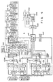
- reference numeral 1 designates a main control unit.
- the main control unit 1 is comprised of a CPU 2 for executing various controls, a floppy disc unit 3 as an administration information memory unit for storing administration information for administrating various file sets (groups of magnetic tapes 14 to be described later) and various files (magnetic tape 14), a title memory 4 for temporarily storing title information read out from an LVR 13 to be described later, a buffer memory 5, for example, a page buffer, having a memory capacity of at least one unit (one page of a document), an MH coding/ decoding unit 6 for compressing the picture information (reducing a redundancy of data) and expanding the compressed one (returning the reduced redundancy to the original one), a size converting circuit 7 for magnifying or reducing the picture information, a mask circuit 8 for electrically masking the picture information, a pattern generator 9 having the pattern information such as characters and/or symbols, and a display interface unit 10.
- a CPU 2 for executing various controls
- Reference numeral 11 designates a read out unit, e.g. a two-dimensional scanning device, which two-dimensionally scans a document 12 to produce electrical signals or picture information corresponding to the picture information on the document 12.
- Reference numeral 13 designates a magnetic tape device (referred to an LVR) with a large memory capacity for sequentially storing (recording) picture information supplied from the two-dimensional scanning device 11 through the main control unit 1, and index information prepared by said main control unit 1 into a storing medium or predetermined memory areas of the magnetic tape.
- Reference numeral 14 designates a plurality of magnetic tapes (cassette tape) of the endless type provided for the kinds of the picture information, which are set in the LVR 13, when necessary.
- a keyboard 15 inputs a title of the picture information and various types of operation commands.
- An output unit 16 e.g. a display unit of the CRT type (referred to as a CRT display unit), displays the picture information supplied through the main control unit 1 from the two- scanning device 11, or, index information and picture information supplied from the LVR 13 through the main control unit 1.
- the output unit 16 cooperates with the display interface unit 10 in the main control unit 1 to form a picture information display unit.
- Another output unit 17 is a hard copy device, for example, and produces in the form of a hard copy 18 the picture information supplied from the two-dimensional scanning device 11 through the main control unit 1 or the index information and the picture information supplied from the LVR 13 through the main control unit 1.
- the page buffer 5, the MH coding/decoding unit 6, the size converting circuit 7, the mask circuit 8, the pattern generator 9, the display interface unit 10, the two-dimensional scanning device 11, the LVR 13, the keyboard 15, the CRT display unit 16 and the hard copy device 17 are connected to a main bus line 20, which provides a main path for data, an address signal, an R/W control signal, and control signals for the memory and the I/0 unit.
- the title memory 4, the page buffer 5, the MH coding/decoding unit 6, the size converting circuit 7, the mask circuit 8, the pattern generator 9, the display interface unit 10, the two-dimensional scanning device 11, the LVR 13, the CRT display unit 16, and the hard copy device 17 are connected to an image bus 30, through which the information is transferred to one another.
- the magnetic tape 14 is called a file, and file names are given to magnetic tapes, respectively, in accordance with the kinds of the picture information stored.
- a group offiles, which belong to the same or similar kind, are called a file set.
- a file set name is also given to the file set.
- the file set name is a generic term and the file name is a specific term.
- a number of picture information recording tracks and a several number of index information recording tracks are formed on the magnetic tape 14 in the running direction. Recorded in the index information recording track are the administration information and various types of the index information.
- the administration information includes a file name, a file set name, a private code, a title structure for determining a title condition set corresponding to the picture information and a title range.
- the administration information is previously recorded into the tape 14 by an operator.
- the index information corresponding to the picture information, includes a title (up to 6 items) and the address information representing memory locations of the picture information.
- the address information includes document size information which is inputted together with the title when the operator inputs the picture information, or the document size information dependent on a document size detecting function of the two-dimensional scanning device 11.
- the document 12 is set in the two-dimensional scanning device 1-1 and one of the magnetic tapes 14 (14a to 14f) is set in the LVR 13.
- the title corresponding to the picture information of the document 12 and a size of the document 12 are keyed in from the keyboard 15 and a memory operation command is keyed in, too.
- the LVR 13 operates to deliver the administration information and all of the index information from the index recording track of the magnetic tape 14, and those information read out are batched into the title memory 4.
- the CPU 2 judges whether or not the administration information in the title memory 4 corresponds to the various types of the administration information stored in the floppy disc device 5.
- the CPU 2 prohibits the image data being stored thereinto. In other words, the CPU 2 judges that the set magnetic tape is not applicable for the document filing system. When the judgment is satisfactory, the CPU 2 judges whether the title inputted is coincident or not with the title of the various types of the index information in the title memory 4. When the judgment is unsatisfactory, it prohibits the storage of the picture information. The storage prohibition is made in order to prevent the same title from being stored in the magnetic tape set in the LVR 13. When the judgment is satisfactory, CPU 2 permits the storage of the picture information corresponding to picture information.
- the two-dimensional scanning device 11 operates to read out the picture information on the document 12 and the read out picture information are stored into the page buffer 5 through the mask circuit 8 and the size converting circuit 7.
- the picture information of one page of the document are stored in the page buffer 5
- the picture information is read out from the page buffer 5 and are supplied to the MH coding/decoding unit 6 where the picture information is data-reduced by a well known modified Hoffmann conversion process, and then are stored in the page buffer 5 again.
- the image data thus data-reduced in the page buffer 5 is supplied through the size converting circuit 7 and the mask circuit 8 to the LVR 13. Then, the information is recorded following the picture information already stored in the picture information recording tracks on the cassette tape 14.
- the CPU 2 judges a memory location of the picture information to be recorded, prepares the index information by using the address information, the title information already inputted, and the document size, and finally adds the index information to the various types of the index information in the title memory 4.
- the administration information and the various types of the index information in the title memory 4 strike through the size converting circuit 7 and the mask circuit 8 for transmission to the LVR 13, and then recorded into the index information recording track of the cassette tape 14. In this case, various index information stored in the index information recording track are updated.
- the magnetic tape 14 storing the desired information is set in the LVR 13. Then, the retrieval/read out operation command is keyed in at the keyboard 15 to operate the LVR 13, so that the administration and various types of index information are read out from the index information recording track of the magnetic tape 14.
- the read out information strikes through the mask circuit 8 and the size converting circuit 7 for transmission to the title memory 4 where those pieces of information are stored in a batch manner.
- the various index information in the title memory 4 strike through the size converting circuit 7 and the mask circuit 8 and are displayed in the CRT display unit 16. In this case, sequence numbers are given to the index information displayed.
- the operator searches the desired picture information from the various index information displayed and keys in a sequence number attached to the index picture information, through the keyboard 15. Then, the index information of the sequence number is selected and the desired picture information is read out from the magnetic tape 14 of the LVR 13 on the basis of the index information.
- the picture information read out passes through the mask circuit 8 and the size converting circuit 7 to be stored in the page buffer 5.
- the picture information is read out from the page buffer 5 and is supplied to the MH coding/ decoding circuit 6.
- the information is data-expanded by the modified Hoffmann decoding process, and then is stored in the page buffer 5.
- the picture information in the page buffer 5 is supplied through the size converting circuit 7 and the mask circuit 8 to the hard copy device 17 where the picture information is reproduced on a recording sheet. If a display command has been keyed in from the keyboard 15, the picture information in the page buffer 5 is supplied through the size converting circuit 7, the mask circuit 8 and the display interface unit 10 to the CRT display unit 16 where the picture information is displayed.
- Fig. 4 illustrates the size conversion circuit 7.
- picture information V sent forth from the two-dimensional scanning device 11 obtained for each scanning line therein or picture information of one line read out of the page buffer 5 is supplied to a data input terminal 400.
- the picture information of one line is assumed to be constituted of 2,048 bits in this case.
- the picture information supplied to the terminal 400 is supplied to a RAM 401 and a latch 406 of six-bit.
- RAM 401 is a 2 Kx1 bit one and the address thereof is designated by the output of a counter 413.
- five RAMs 401 to 405 and seven latches 406 to 412 are provided.
- RAMs 401 to 405 and latches 406 to 412 are all operated by a clock signal supplied from a main clock generator 44 through a signal path shown by a solid line or a signal line shown by a two-dot line.
- the signal path of solid line is used when the circuit of Fig. 4 acts as a size reduction circuit and the signal path of two-dot line is for a size expansion circuit.
- first one line picture information of 2,048 bits is stored in the first RAM 401. Then, when a first bit of second line picture information is supplied to the RAM 401 the first bit of the first line picture information having been stored in the RAM 401 is read out therefrom and latched at the latch 406, while the first bit of the second line is stored in the first memory location of RAM 401. Then, the second bit of the second line is stored in the RAM 401 and the second bit of the first line is read out and latched in the latch 404. In the same time the first bit of the first line latched at the latch 407 is sent forth to the second RAM 402 and stored therein.
- each first bit of first to sixth lines latched at the latch 407 is sent forth to the next latch 408 and each second bit of first to sixth lines is latched at latch 407.
- seventh bit of sixth line picture information is supplied to the terminal 400
- the first lilt of each first to sixth line is latched at latch 412
- second bit of the same is latched at latch 411
- third bit at latch 410 the fourth bit at latch 409
- Two adders 416, 417, two latches 418, 419, a comparator 420 and the counter 413 are constituting a distance calculating circuit 430 in X direction, and, two adders 421, 422, two latches 423, 424, a comparator 425 and a counter 426 constitute a distance calculating circuit 431 in Y direction.
- These distance calculating circuits 430 and 431 are used for calculating a picture dot position of a size-converted picture in both X, Y directions.
- the size conversion (expansion or reduction) rate setting data in X, Y directions supplied from CPU 2 is supplied to adders 416, 417, 421 and 422.
- reductive ratio data is shown as an example.
- the integer part of the reduction rate is supplied to adders 416, 421 and a decoder 427 and the fraction part is supplied to adders 417 and 422.
- the outputs of adders 416, 417, 421 and 422 are supplied to the latches 418, 419, 423 and 424, respectively.
- the outputs of the latches 418 and 423 are respectively supplied to one input side of the comparator 420 and 425 and also fedback to input side of the adders 416 and 421, respectively.
- the other sides of the comparators 420 and 425 have inputs supplied from the counters 413 and 426.
- the outputs of latches 419 and 423 are fedback to the input sides of the adders . 417 and 421, respectively.
- the output data read out of the arithmetic ROM 415 is supplied to one input side of a comparator 432 which has the other input side supplied with a slice level data obtained from a slice level data generator 433.
- the coincidence signal of the comparator 432 is supplied to a D input terminal of a flip-flop 434 having a clock terminal CL supplied with an output of an AND gate 435.
- the AND gate 435 has one input supplied with a coincidence output XCOM of the comparator 420 while the other input has an input YCOM obtained from the comparator 425.
- picture dot positions of the original picture are designated by the symbol "x" while the picture dot positions of the size-converted picture are designated by the black dot.
- the picture dot at the position (i, j) on the original picture is defined as ⁇ P i , j ⁇ .
- the picture dot at the position (I, J) on the size-reduced picture is defined as
- the distance between two adjacent picture dots of the original picture is defined as 1. Then the distance between two adjacent size-reduced dots on the original picture equals with the reduction ratio Rr.
- the constant L is set as 4.5.
- the average gray level ⁇ i, J of S is calculated based upon the fact whether the picture dot ⁇ P i , j ⁇ belonging to the area S exists or not. If the distance between the respective original position P i, j and the converted position P i , J is defined as r,, j , the weighting factor a,, j for calculating the average gray level ⁇ i, J is so determined that the factor ⁇ i, j is inversely proportional to the distance r l , j .
- the factor ⁇ i, j is represented as follows.
- the average gray level ⁇ i, J is obtained. Then, the converted picture dot is obtained by using a predetermined slice level 6.
- the integer part 4 of the reductive ratio supplied from CPU 2 is supplied to the latch 418 through adder 416.
- a coincidence signal XCOM is delivered from the comparator 420 and is supplied to latches 418 and 419 and AND gate 435.
- the fraction part 0.5 is latched at latch 419 through adder 417.
- magnifying ratio of, for example, 0.5 is supplied to the adders 416, 417, 421, 422 from the CPU 2.
- the number of Q, is twice the number of P I , j and the original picture size is magnified by two times.
- Mask circuit The circuit masks the unnecessary portion of the picture information and operates the following operation under control of the CPU 2.
- Fig. 7 shows the mask circuit 8.
- Down counters 51 and 52 are an X direction nonmask counter and an X direction nonmask counter, as first counters. Those counters count the clock signal D corresponding to each bit (serving as a picture element of the picture information) is one-dimensional direction of the two-dimensional scanning device 11 or the clock signal D corresponding to one picture element of the picture information read out from the page buffer 5 every scanning line (corresponding to the line scanning of the two-dimensional scanning device 11).
- F designates a scanning area of the two-dimensional scanning device 11 an the document 12 is set in the scanning area F.
- the first mask area in the X direction is a distance X1
- a nonmask area (an effective area) is a distance X2-X1.
- the first mask area in the Y direction is a distance Y1 and a nonmask area (an effective area) is a distance Y2-Y1.
- a value of X1 is preset in the counter 51 and a value of X2-X1 is preset in the counter 52.
- Decoders 53 and 55 produce logical "1" signals when the contents of the counters 51 and 52 are logical "0".
- Down- counters 55 and 56 are a Y direction counter and a Y direction nonmask counter as second counters, respectively. Those counters count a line clock signal E every line scanning in the Y direction of the two-dimensional scanning device 11 and another line clock signal E every line scanning for the picture information read out from the page buffer 5 every line.
- a value Y1 is preset in the counter 55 and a value of Y1-Y2 is preset in the counter 56.
- Decoders 57 and 58 produce logical "1" signals when the contents of the counters 55 and 56 are "0".
- a gate circuit 59 makes a mask or nonmask of a picture information signal V supplied from the two-dimensional scanning device 11 and another picture information signal V supplied from the page buffer 5.
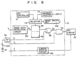
- the circuit 10 as shown in Fig. 9, is comprised of a picture information rotating circuit 60 for rotating the picture information every 90°.
- the picture information V delivered from the rotating circuit 60 is supplied to a refresh memory unit having a first refresh memory 75 and a second refresh memory 76.
- a start address of the refresh memory unit is selected by the selector 73 which is driven by an output of an image switch key 102.
- the image switch key 102 is provided of an operation keyboard as shown in Fig. 13.
- the selector 73 receives outputs of a CRT controller 71 and an address counter 72 supplied with an address designation signal from CPU 2.
- the picture information V read out from the page buffer 5 and reduced by the size converting circuit 7 are rotated by a given angle, if necessary, by the picture information rotating circuit 60, and are stored into the first refresh memory 75.
- the picture information read out from the first refresh memory 75 are supplied through the phase determining circuit 77 to the CRT display unit 16 where the information are displayed.
- the cursor display device 80 when a cursor of a predetermined size is set for the picture information of the CRT display device 16, or the picture information in the first refresh memory 75, by the cursor display device 80, the picture information of the area corresponding to the cursor is read out from the page buffer 5, and the read out information is properly reduced by the size converting circuit 7 to be stored in the second refresh memory 76 under the address designation of the CPU 2 through the address counter 72.
- the phase determining circuit 77 is comprised of an exclusive OR circuit 78 and an AND circuit 79.
- the exclusive OR circuit 78 is supplied with the picture information read out from either the first refresh memory 75 or the second refresh memory 76 and a phase signal H keyed in by an inversion key 100 on the keyboard 15 shown in Fig. 13 as well via a flip-flop 74.
- the phase signal H is a signal of logic "1" or "0" from the flip-flop circuit FF.
- the color (while, black) of the picture display over the entire display screen of the CRT display device 16 can be freely inverted.
- the AND circuit 79 is supplied with the picture information signal from the exclusive OR circuit 78 and an unblanking signal I from the CRT controller 71. In other words, an effective display area of the picture information for the CRT display device 16 can be set by the unblanking signal
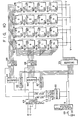
- Fig. 10 shows a picture information rotating circuit.
- a decoder 62 which produces four types (0°, 90°, 180° and 270°) of rotation commands in response to an angle designating signal R of 2 bits from a scale-of-four counter 60 stepped through the operation of a rotation key 101; for example, "0, 0" for 0°, "0, 1” for 90°, "1, 0" for 180°, and "1,1" for 270°.
- Reference numeral 63 is a selector circuit for producing a clock signal D corresponding to each bit (picture element) every line of the picture information and a line clock signal E corresponding to each line of the picture information for transmission to the output line according to the rotating commands of 0° and 180° from the decoder 62.
- Numeral 64 designates a scale-of-128 counter; 65 a scale-of-four counter; 66 a scale-of-128 counter; 67 a scale-of-four counter.
- Reference numeral 68 is a gate circuit which is enabled when receiving the rotating commands of 90° and 180°. With this, the addresses of the RAMs 61-11 to 61-44 in the X direction are sequentially designated.
- a gate circuit 69 is enabled by rotating commands of 270° and 180°, to sequentially designate addresses in the X and Y directions of the RAMs 61 -11 to 61-44.
- Reference numeral 70 is a decoder for outputting a chip select signal in response to outputs of the counters 65 and 67 and the angle designating signal R to select the RAMs 61-11 to 61-44.
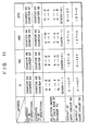
- Fig. 11 is useful in explaining how the circuit shown in Fig. 10 practically operates.
- the picture information can be displayed rotated at a desirable rotating angle by inputting the rotating command corresponding to the predetermined angle from the keyboard 15.
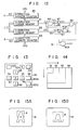
- Fig. 12 shows a cursor display device 80.
- reference numeral 81 designates an X direction cursor memory for holding a positional information on both sides of the cursor in response to a write code information J from the CPU 2.
- Reference numeral 81 is a Y direction cursor memory for holding both the top and bottom positional information of the cursor in response to the write code information J from the CPU 2.
- Numeral 83 indicates an X direction address counter which counts a cursor clock signal P supplied from the first refresh memory 75.
- a Y direction address counter 84 counts a horizontal sync signal Q supplied from the first refresh memory 75.
- Numeral 85 represents a decoder which produces a logic "1" signal when the contents of the counter 83 are coincident with the positional information signals of the both sides.
- Reference numeral 86 designates a decoder for producing a logic "1" signal when the contents of the counter 84 are coincident with the positional information of the top and bottom sides.
- Reference numerals 87 and 88 are T flip-flop; 89 an OR circuit; 901,902 and 903 AND circuits.
- Character W indicates a blink signal; CV a cursor video signal.
- reference numeral 92 designates an operation panel provided on the keyboard 15.
- 93, 94, 95 and 96 are shift keys, and when those keys are pushed, shift pulses are produced during the pushed period.
- Reference numeral 97 indicates a shift key for shifting the cursor to the left upper corner of the display screen; 98 a magnifying key for magnifying the cursor and a pulse is generated every time the key is pushed; 99 a reducing key for reducing the cursor and producing a pulse every time the key is pushed.
- Reference numeral 100 designates an inversion key of black and white; 101 a rotating key. One push of the rotating key steps the counter 60 by +1 to make a 90° rotation of the picture clockwise.
- Fig. 14 shows predetermined sizes S1, S2, S3 and S4 of the cursor.
- Fig. 15A shows a display state of the cursor S.
- the picture information read out from the first refresh memory is displayed and the cursor S corresponds to the predetermined part of the picture information.
- the partial picture information is stored in the second refresh memory 76 as described above, and is displayed as shown in Fig. 15B.
- Fig. 16 shows how the above operation is practically performed.
- (a) indicates a cursor clock signal P, (b) a horizontal sync signal Q, (c) an output of the decoder 85, (d) an output of the decoder 86, (e) an output of the AND circuit 901, (f) an output of the T-flip-flop 87, (g) an output of the T-flip-flop 88, (h) an output of the AND circuit 902 and (i) an output of the OR circuit 89.
- the present invention is applicable not only for the document filing system, but applicable for any type of devices requiring a picture display.
- the present invention is provided with the picture information rotating circuit for producing the picture at a given rotating angle.
- the picture information outputted from the picture information rotating circuit is stored in the refresh memory and the contents of the refresh memory are displayed in the display section. Therefore, when the document is set in any direction in storing the picture information of the document, the picture information read out can always be displayed in a correct way, not inverted or brought-down way. Additionally, the picture information display device can display the picture information at any desired rotational angle.
Landscapes
- Engineering & Computer Science (AREA)
- Signal Processing (AREA)
- General Physics & Mathematics (AREA)
- Theoretical Computer Science (AREA)
- Multimedia (AREA)
- Physics & Mathematics (AREA)
- Computer Hardware Design (AREA)
- Editing Of Facsimile Originals (AREA)
- Processing Or Creating Images (AREA)
- Image Processing (AREA)
- Information Retrieval, Db Structures And Fs Structures Therefor (AREA)
- Television Signal Processing For Recording (AREA)
- Storing Facsimile Image Data (AREA)
Description
- This invention relates to a document filing system which sequentially stores picture information on a document etc. in a memory unit and retrieves any desired one, as required, from the various picture information stored to permit it to be read out.
- A document filing system has been developed and put to practical use, which reads out picture information on a document etc., currently available in large quantity, through two-dimensional optical scanning, retrieves, and reads out, any desired one, as required, from the various picture information stored, and delivers it to an output unit, such as a CRT display device or a printing device, for display in a viewable state.
- In such system, a CRT display device with too large a screen cannot be used due to a restriction on a cost and a space factor. For this reason, the picture information is displayed to a reduced scale which is smaller than the original dimension of a document. By so doing, it is possible to display a whole picture image, corresponding to one page of an A4 sized document, on the screen of a CRT display unit. Since, however, 525 scanning lines are used in the CRT display unit, poor resolution results and, for the small characters on the document, there are cases where it is often impossible to read out such characters as they are.
- It is accordingly the object of this invention to provide a document filing system which can freely vary the size of a document picture on the screen of a CRT display unit, while displaying a desired portion of the document picture in an enlarged state.
- According to this invention there is provided a document filing system comprising means for reading out picture information on a document, means for storing the picture information so read out, and means for retrieving the stored picture information and for reading out any desired picture information, the document filing system further including a buffer memory for temporarily storing the picture information so read out, a size conversion circuit for performing the magnifying or reducing of the picture information which is read out from the buffer memory, a refresh memory for storing the picture information obtained from the size conversion circuit, a display unit for displaying the picture information stored in the refresh memory, a cursor display unit for setting a cursor of a predetermined size with respect to the picture information in the refresh memory which is to be displayed on the screen of the display unit, and control means for causing the picture information enclosed by the cursor to be read from the buffer memory, in which the picture information read out by the control means is displayed on the screen of the display unit.
- This invention can be more fully understood from the following detailed description when taken in conjunction with the accompanying drawings, in which:
- Fig. 1 is a block diagram of a document filing system with a display device assembled thereinto;
- Fig. 2 is a block diagram illustrating detailed arrangement of the document filing system shown in Fig. 1;
- Fig. 3 is a block diagram of a peripheral circuit including a compression/expansion circuit of data lengths;
- Fig. 4 is a block diagram of a size converting circuit;
- Figs. 5 and 6 are schematic diagrams useful in explaining the operation of the size converting circuit shown in Fig. 4;
- Fig. 7 is a block diagram illustrating an arrangement of a mask circuit;
- Fig. 8 is a schematic diagram illustrating a relationship between a scanning area and a document size of a document read out device;
- Fig. 9 is a block diagram of a display device according to the present invention;
- Fig. 10 is a block diagram of a picture rotating circuit used in the display device in Fig. 9;
- Fig. 11 is a table in aid of explaining the operation of the circuit shown in Fig. 10;
- Fig. 12 is a block diagram of a cursor display circuit used in the circuit in Fig. 9;
- Fig. 13 is a plan view of a picture operating section on a keyboard;
- Fig. 14 is a view illustrating sizes of a cursor;
- Figs. 15A and 15B are views illustrating cursor display states; and
- Fig. 16 is a time chart useful in explaining the operation of the circuit shown in Fig. 12.
- In a document filing system shown in Figs. 1 and 2,
reference numeral 1 designates a main control unit. Themain control unit 1 is comprised of aCPU 2 for executing various controls, afloppy disc unit 3 as an administration information memory unit for storing administration information for administrating various file sets (groups of magnetic tapes 14 to be described later) and various files (magnetic tape 14), atitle memory 4 for temporarily storing title information read out from anLVR 13 to be described later, abuffer memory 5, for example, a page buffer, having a memory capacity of at least one unit (one page of a document), an MH coding/decoding unit 6 for compressing the picture information (reducing a redundancy of data) and expanding the compressed one (returning the reduced redundancy to the original one), asize converting circuit 7 for magnifying or reducing the picture information, amask circuit 8 for electrically masking the picture information, apattern generator 9 having the pattern information such as characters and/or symbols, and adisplay interface unit 10.Reference numeral 11 designates a read out unit, e.g. a two-dimensional scanning device, which two-dimensionally scans adocument 12 to produce electrical signals or picture information corresponding to the picture information on thedocument 12.Reference numeral 13 designates a magnetic tape device (referred to an LVR) with a large memory capacity for sequentially storing (recording) picture information supplied from the two-dimensional scanning device 11 through themain control unit 1, and index information prepared by saidmain control unit 1 into a storing medium or predetermined memory areas of the magnetic tape. Reference numeral 14 designates a plurality of magnetic tapes (cassette tape) of the endless type provided for the kinds of the picture information, which are set in theLVR 13, when necessary. Akeyboard 15 inputs a title of the picture information and various types of operation commands. Anoutput unit 16, e.g. a display unit of the CRT type (referred to as a CRT display unit), displays the picture information supplied through themain control unit 1 from the two-scanning device 11, or, index information and picture information supplied from theLVR 13 through themain control unit 1. Theoutput unit 16 cooperates with thedisplay interface unit 10 in themain control unit 1 to form a picture information display unit. Anotheroutput unit 17 is a hard copy device, for example, and produces in the form of ahard copy 18 the picture information supplied from the two-dimensional scanning device 11 through themain control unit 1 or the index information and the picture information supplied from theLVR 13 through themain control unit 1. - The
page buffer 5, the MH coding/decoding unit 6, thesize converting circuit 7, themask circuit 8, thepattern generator 9, thedisplay interface unit 10, the two-dimensional scanning device 11, theLVR 13, thekeyboard 15, theCRT display unit 16 and thehard copy device 17 are connected to a main bus line 20, which provides a main path for data, an address signal, an R/W control signal, and control signals for the memory and the I/0 unit. Thetitle memory 4, thepage buffer 5, the MH coding/decoding unit 6, thesize converting circuit 7, themask circuit 8, thepattern generator 9, thedisplay interface unit 10, the two-dimensional scanning device 11, theLVR 13, theCRT display unit 16, and thehard copy device 17 are connected to an image bus 30, through which the information is transferred to one another. - In the document filing system, the magnetic tape 14 is called a file, and file names are given to magnetic tapes, respectively, in accordance with the kinds of the picture information stored. A group offiles, which belong to the same or similar kind, are called a file set. A file set name is also given to the file set. The file set name is a generic term and the file name is a specific term. A number of picture information recording tracks and a several number of index information recording tracks are formed on the magnetic tape 14 in the running direction. Recorded in the index information recording track are the administration information and various types of the index information. The administration information includes a file name, a file set name, a private code, a title structure for determining a title condition set corresponding to the picture information and a title range. The administration information is previously recorded into the tape 14 by an operator. The index information, corresponding to the picture information, includes a title (up to 6 items) and the address information representing memory locations of the picture information. In this case, the address information includes document size information which is inputted together with the title when the operator inputs the picture information, or the document size information dependent on a document size detecting function of the two-
dimensional scanning device 11. - A short description as to how the document filing system thus constructed operates, will now be given.
- In a first step, the
document 12 is set in the two-dimensional scanning device 1-1 and one of the magnetic tapes 14 (14a to 14f) is set in theLVR 13. The title corresponding to the picture information of thedocument 12 and a size of thedocument 12 are keyed in from thekeyboard 15 and a memory operation command is keyed in, too. In response to the keying in those information, the LVR 13 operates to deliver the administration information and all of the index information from the index recording track of the magnetic tape 14, and those information read out are batched into thetitle memory 4. At this time, theCPU 2 judges whether or not the administration information in thetitle memory 4 corresponds to the various types of the administration information stored in thefloppy disc device 5. When the judgment is unsatisfactory, theCPU 2 prohibits the image data being stored thereinto. In other words, theCPU 2 judges that the set magnetic tape is not applicable for the document filing system. When the judgment is satisfactory, theCPU 2 judges whether the title inputted is coincident or not with the title of the various types of the index information in thetitle memory 4. When the judgment is unsatisfactory, it prohibits the storage of the picture information. The storage prohibition is made in order to prevent the same title from being stored in the magnetic tape set in theLVR 13. When the judgment is satisfactory,CPU 2 permits the storage of the picture information corresponding to picture information. - In this way, the two-
dimensional scanning device 11 operates to read out the picture information on thedocument 12 and the read out picture information are stored into thepage buffer 5 through themask circuit 8 and thesize converting circuit 7. When the picture information of one page of the document are stored in thepage buffer 5, the picture information is read out from thepage buffer 5 and are supplied to the MH coding/decoding unit 6 where the picture information is data-reduced by a well known modified Hoffmann conversion process, and then are stored in thepage buffer 5 again. The image data thus data-reduced in thepage buffer 5 is supplied through thesize converting circuit 7 and themask circuit 8 to theLVR 13. Then, the information is recorded following the picture information already stored in the picture information recording tracks on the cassette tape 14. At this time, theCPU 2 judges a memory location of the picture information to be recorded, prepares the index information by using the address information, the title information already inputted, and the document size, and finally adds the index information to the various types of the index information in thetitle memory 4. The administration information and the various types of the index information in thetitle memory 4 strike through thesize converting circuit 7 and themask circuit 8 for transmission to theLVR 13, and then recorded into the index information recording track of the cassette tape 14. In this case, various index information stored in the index information recording track are updated. - For retrieving and reading out desired picture information from the various picture information stored, the magnetic tape 14 storing the desired information is set in the
LVR 13. Then, the retrieval/read out operation command is keyed in at thekeyboard 15 to operate theLVR 13, so that the administration and various types of index information are read out from the index information recording track of the magnetic tape 14. The read out information strikes through themask circuit 8 and thesize converting circuit 7 for transmission to thetitle memory 4 where those pieces of information are stored in a batch manner. At this time, when a sort command is keyed in from thekeyboard 15, the various index information in thetitle memory 4 strike through thesize converting circuit 7 and themask circuit 8 and are displayed in theCRT display unit 16. In this case, sequence numbers are given to the index information displayed. Then, the operator searches the desired picture information from the various index information displayed and keys in a sequence number attached to the index picture information, through thekeyboard 15. Then, the index information of the sequence number is selected and the desired picture information is read out from the magnetic tape 14 of theLVR 13 on the basis of the index information. The picture information read out passes through themask circuit 8 and thesize converting circuit 7 to be stored in thepage buffer 5. When one page picture information is stored in thepage buffer 5, the picture information is read out from thepage buffer 5 and is supplied to the MH coding/decoding circuit 6. In thecircuit 6, the information is data-expanded by the modified Hoffmann decoding process, and then is stored in thepage buffer 5. At this time, if the record command has been keyed in by thekeyboard 15, the picture information in thepage buffer 5 is supplied through thesize converting circuit 7 and themask circuit 8 to thehard copy device 17 where the picture information is reproduced on a recording sheet. If a display command has been keyed in from thekeyboard 15, the picture information in thepage buffer 5 is supplied through thesize converting circuit 7, themask circuit 8 and thedisplay interface unit 10 to theCRT display unit 16 where the picture information is displayed. - The explanation to follow is the elaboration of the MH coding/
decoding circuit 6, thesize converting circuit 7, themask circuit 8 and thedisplay interface circuit 10. - (1) MH coding/decoding circuit 6: The
circuit 6 has the following functions under control of theCPU 2, in addition to the data compression (coding) and expansion (decoding) as its main function. It is assumed that the memory capacity of thepage buffer 5 corresponds to the picture information of a document of A4 size. In storing the picture information, if thedocument 12 has a B5 size smaller than the A4 size, some memory areas of thepage buffer 5 store no picture information. Therefore, if the picture information is compressed over all the memory areas of thepage buffer 5, the unnecessary information is also stored in theLVR 13. It is for this reason that theCPU 2 controls the MH coding/decoding operation of thecircuit 6 in accordance with the document size information, and reduces only the picture information corresponding to the B5 size stored in thepage buffer 5. Fig. 3 shows a detailed peripheral circuit of thepage buffer 5 and the MH coding/decoding circuit 6. Aline buffer 31 temporarily stores the picture information of one line read out from thepage buffer 5 or the picture information of one line to be stored in thepage buffer 5. Atiming signal generator 32 generates a clock signal D corresponding to one picture element of the picture information and a line clock signal E corresponding to one line. Anaddress counter 33 designates an effective area in theline buffer 31 corresponding to the size of thedocument 12.Holders selector circuit 37 selects output signals from theholders document 12 on the basis of a command signal CMD issued from theCPU 2. Specifically, when the CMD is "0", an AND gate connected to theholder 35 is enabled through an inverter to fetch the size data of the A4 size. Acomparator 34 compares the output from theaddress counter 33 with that of theselector circuit 37. An end-of-line (EOL) detector circuit 38 controls thetiming generating circuit 32 in accordance with the comparing result of thecomparator 34. - (2) Size converting circuit 7: The
circuit 7 has a magnifying mode, a reduction mode, and a strikethrough mode, and operates in the following under control of theCPU 2.- (a) In storing the picture information; the
circuit 7 reduces or permits the strike-through of the picture information supplied from the two-dimensional scanning device 11 to thepage buffer 5. For example, if the memory capacitor of thepage buffer 5 corresponds to the picture information of the A4 document, it is impossible to store the picture information of the B4 size document. It is for this reason that theCPU 2 drives thesize converting circuit 7 to operate to reduce the picture information at a given reduction rate when the document size information inputted from the two-dimensional scanning device 11 or thekeyboard 15 is larger than the memory capacity of thepage buffer 5. Therefore, there is no need to use the page buffer with a large memory capacity, thereby to prevent the increase of the manufacturing cost and the expansion of a space occupying by it in the chip. When the document size is equal to or smaller than the memory capacity of the page buffer, for example, the size of the document, is A4 or B5, thesize converting circuit 7 is driven by theCPU 2 to execute the strike-through operation (the reduction rate is "0" and the expansion or magnification rate is "0"). - (b) In storing and reading out the picture information; the
circuit 7 executes the strike-through of the picture information supplied from thepage buffer 5 to theLVR 13 and the picture information from theLVR 13 to thepage buffer 5. - (c) In recording the read out picture information by the
hard copy device 17; thecircuit 7 magnifies, reduces or strike-throughs the picture information from thepage buffer 5 to thehard copy device 17. Specifically, theCPU 2 drives thecircuit 7 to magnify at a given magnifying rate or to permit the strike-through of the picture information in accordance with the document size information contained in the index information selected when the picture information is read out. The magnifying operation in this case is made for returning the picture information reduced in item (a) to the original size of the picture information. TheCPU 2 activates the size magnification/reduc-tion circuit 7 to reduce at a given reducing rate or to permit the strike-through of the picture information in accordance with the size of the recording paper in the hard copyingdevice 17. In this way, the read out picture information of one unit may reliably be recorded regardless of the size of the recording paper in thehard copy device 17. - (d) In displaying the read out picture information by the
CRT display unit 16; thecircuit 7 reduces or permits the strike-through of the picture information from thepage buffer 5 to thedisplay interface 10. TheCPU 2 actuates thesize converting circuit 7 to reduce at a given reduction rate or permit strike-through of the picture information on the basis of the display size ability of theCRT display unit 16 previously stored. Therefore, there is no need of using a bulky and high performance CRT display unit and hence it is possible to prevent the increase of its manufacturing cost. In this case, through the operation by the operator, thesize converting circuit 7 may be driven, to provide an easy-to-see display. - (e) Others; the
size converting circuit 7 operates in the strike-through mode when the pattern information read out from thepattern generator 9 is supplied to thepage buffer 5 and is added to the picture information in thepage buffer 5.
- (a) In storing the picture information; the
- Fig. 4 illustrates the
size conversion circuit 7. In this Figure, picture information V sent forth from the two-dimensional scanning device 11 obtained for each scanning line therein or picture information of one line read out of thepage buffer 5 is supplied to adata input terminal 400. The picture information of one line is assumed to be constituted of 2,048 bits in this case. The picture information supplied to the terminal 400 is supplied to aRAM 401 and a latch 406 of six-bit.RAM 401 is a 2 Kx1 bit one and the address thereof is designated by the output of acounter 413. In thecircuit 7, fiveRAMs 401 to 405 and seven latches 406 to 412 are provided. TheseRAMs 401 to 405 and latches 406 to 412 are all operated by a clock signal supplied from a main clock generator 44 through a signal path shown by a solid line or a signal line shown by a two-dot line. The signal path of solid line is used when the circuit of Fig. 4 acts as a size reduction circuit and the signal path of two-dot line is for a size expansion circuit. - Thus, under the address control of the
counter 413, first one line picture information of 2,048 bits is stored in thefirst RAM 401. Then, when a first bit of second line picture information is supplied to theRAM 401 the first bit of the first line picture information having been stored in theRAM 401 is read out therefrom and latched at the latch 406, while the first bit of the second line is stored in the first memory location ofRAM 401. Then, the second bit of the second line is stored in theRAM 401 and the second bit of the first line is read out and latched in thelatch 404. In the same time the first bit of the first line latched at thelatch 407 is sent forth to the second RAM 402 and stored therein. In this way, when the last (2,048th) bit of second line is stored inRAM 401, the first one line picture information data of 2,048 bits is shifted to second RAM 402. Thus, each one line picture information of 2,048 bits is sequentially shifted in theRAMs 401 to 405. At last, first to fifth line picture information is respectively stored in theRAMs 405 to 401 and first bits of each first to fifth line picture information are latched at the latch 406 to be sent forth to thelatch 407 at the same time together with a first bit of sixth line picture information supplied to the terminal 400. - When the second bit of the sixth line is supplied to the terminal 400, each first bit of first to sixth lines latched at the
latch 407 is sent forth to thenext latch 408 and each second bit of first to sixth lines is latched atlatch 407. In the similar manner, when seventh bit of sixth line picture information is supplied to the terminal 400, the first lilt of each first to sixth line is latched atlatch 412, second bit of the same is latched atlatch 411, third bit atlatch 410, fourth bit atlatch 409, fifth bit atlatch 408, and sixth bit atlatch 407. Thus, if rearranged the respective bits latched in thelatches 407 to 412 in a matrix array, the original picture is reproduced as the dot picture as shown in Fig. 5 wherein the black dots represent "1" bit and white dots represent "0" bit. Thus, a local picture information of 6 bits (X direction)x6 lines (Y direction) is supplied to anarithmetic ROM 415 from thelatches 407 to 412. - Two
adders latches comparator 420 and thecounter 413 are constituting adistance calculating circuit 430 in X direction, and, twoadders latches distance calculating circuit 431 in Y direction. Thesedistance calculating circuits CPU 2 is supplied toadders adders decoder 427 and the fraction part is supplied toadders adders latches latches comparator 420 and 425 and also fedback to input side of theadders comparators 420 and 425 have inputs supplied from thecounters 413 and 426. The outputs oflatches adders - Three bits in fraction part output data of the
circuit 430 and three bits in fraction part output data of thecircuit 431 are took out from therespective latches arithmetic ROM 415 as an address designating signal. The output data read out of thearithmetic ROM 415 is supplied to one input side of acomparator 432 which has the other input side supplied with a slice level data obtained from a slicelevel data generator 433. The coincidence signal of thecomparator 432 is supplied to a D input terminal of a flip-flop 434 having a clock terminal CL supplied with an output of an ANDgate 435. The ANDgate 435 has one input supplied with a coincidence output XCOM of thecomparator 420 while the other input has an input YCOM obtained from the comparator 425. - The operation of the
size conversion circuit 7 shown in Fig. 4 will be described in detail by referring to Fig. 6. It is assumed that the reduction ratio designated from theCPU 2 is 1/4.5. Thus, the integer part of the reduction ratio is 4 while the fraction part thereof is 0.5. These numeral data in digital form is respectively set in theadders - In Fig. 6, picture dot positions of the original picture are designated by the symbol "x" while the picture dot positions of the size-converted picture are designated by the black dot. The picture dot at the position (i, j) on the original picture is defined as {Pi, j}.

- The picture dot at the position (I, J) on the size-reduced picture is defined as

- The distance between two adjacent picture dots of the original picture is defined as 1. Then the distance between two adjacent size-reduced dots on the original picture equals with the reduction ratio Rr.

- In this case the constant L is set as 4.5. When LxL area having a center position Qi, J is designated as S, the average gray level φi, Jof S is calculated based upon the fact whether the picture dot {Pi,j} belonging to the area S exists or not. If the distance between the respective original position Pi, j and the converted position Pi,Jis defined as r,, j, the weighting factor a,, j for calculating the average gray level φi, J is so determined that the factor αi, j is inversely proportional to the distance rl, j. Thus, by setting the factor a,, j as 1 at the position of Q,, j, and as 0.5 at the position away from by U2, the factor αi, j is represented as follows.

- Therefore, the average gray level φi, J


predetermined slice level 6. - Now the operation of the circuit of Fig. 4 will be described. The
integer part 4 of the reductive ratio supplied fromCPU 2 is supplied to thelatch 418 throughadder 416. Thus, when the contents ofcounter 413 becomes 4, a coincidence signal XCOM is delivered from thecomparator 420 and is supplied tolatches gate 435. On the other hand, the fraction part 0.5 is latched atlatch 419 throughadder 417. Thus, when the signal XCOM is supplied to thelatches adder 417 and a carry signal of 1 is supplied to theadder 416. Accordingly, an addition of 4+4+1=9 is done at theadder 416 and a new data "9" is set at thelatch 418. In this time, when the contents of thecounter 413 becomes "9", an output XCOM is obtained at the output of thecomparator 420. Then 9+4=13 is set at thelatch 418 and an output XCOM is obtained when thecounter 413 reaches at 13. At this time, an addition of 13+4+1 is done at theadder 416 and a new data "18" is set at thelatch 418. Thus, each time the contents of thecounter 413 becomes "4, 9, 13, 18, 22, 27, ..." an output XCOM is obtained at thecomparator 420. This output XCOM is supplied to one input of the ANDgate 435. - The same operation as in the
circuit 430 is performed in thecircuit 431 and an output YCOM is supplied to the other input of the ANDgate 435 from the comparator 425 every time the contents of the counter 426 reach at "4, 9, 13, 18, 22, 27, ...". When both the inputs XCOM and YCOM are supplied to the ANDgate 435, an output is supplied to the clock terminal of the flip-flop 434. At this time, if the output level φi, J coincide with an output level of theslice level generator 433, an output is supplied from thecomparator 432 to the D terminal of the flip-flop 434, and an output Q,, of black dot as shown in Fig. 6 is obtained from the flip-flop 434. - In the magnifying operation, magnifying ratio of, for example, 0.5 is supplied to the
adders CPU 2. In this case, the number of Q,, is twice the number of PI, j and the original picture size is magnified by two times. - (3) Mask circuit: The circuit masks the unnecessary portion of the picture information and operates the following operation under control of the
CPU 2. - (a) In storing the picture information; the circuit masks the picture information read out by the two-
dimensional scanning device 11 and supplied to thepage buffer 5 in accordance with the document size information inputted. Since the two-dimensional scanning device 11 scans a given scanning area irrespective of the size of thedocument 12, only the area corresponding to the size of thedocument 12 is treated as the effective picture information. Therefore, the unnecessary picture information such as scars or dust are negligible. Stored into thepage buffer 5 are new picture information and the apparent picture information around the former (the portion masked) as well. Accordingly, even if the old picture information is stored in thepage buffer 5, the old information is never added to the new picture information. Accordingly, there is no need for control for previously clearing thepage buffer 5. - (b) In reading out the picture information; the mask circuit masks the picture information read out from the
page buffer 5 in accordance with the document size information contained in the index information selected and supplies it to thehard copy device 17 or theinterface 10. In this case, in thehard copy device 17, no unnecessary toner is attached to a photosensitive drum (not shown), thereby to lessen soil on the drum. - Fig. 7 shows the
mask circuit 8. Down counters 51 and 52 are an X direction nonmask counter and an X direction nonmask counter, as first counters. Those counters count the clock signal D corresponding to each bit (serving as a picture element of the picture information) is one-dimensional direction of the two-dimensional scanning device 11 or the clock signal D corresponding to one picture element of the picture information read out from thepage buffer 5 every scanning line (corresponding to the line scanning of the two-dimensional scanning device 11). In Fig. 8, F designates a scanning area of the two-dimensional scanning device 11 an thedocument 12 is set in the scanning area F. In this case, the first mask area in the X direction is a distance X1 and a nonmask area (an effective area) is a distance X2-X1. The first mask area in the Y direction is a distance Y1 and a nonmask area (an effective area) is a distance Y2-Y1. A value of X1 is preset in thecounter 51 and a value of X2-X1 is preset in the counter 52.Decoders counters 51 and 52 are logical "0". Down-counters 55 and 56 are a Y direction counter and a Y direction nonmask counter as second counters, respectively. Those counters count a line clock signal E every line scanning in the Y direction of the two-dimensional scanning device 11 and another line clock signal E every line scanning for the picture information read out from thepage buffer 5 every line. Accordingly, a value Y1 is preset in thecounter 55 and a value of Y1-Y2 is preset in the counter 56.Decoders counters 55 and 56 are "0". Agate circuit 59 makes a mask or nonmask of a picture information signal V supplied from the two-dimensional scanning device 11 and another picture information signal V supplied from thepage buffer 5. Thus, in the X direction, thecounter 51 counts down and when the counts thereof reaches "0", the counter 52 starts to count down. When the contents of the counter 52 becomes "0", thecounters 51 and 52 are preset again, and ready for the next line scanning. In the Y direction, thecounter 55 counts down, and when the contents thereof becomes "0", the counter 56 starts to count down. When the contents of the counter 56 is "0", thecounters 55 and 56 are preset again and ready for the next line scanning. - (4) Display interface: The
circuit 10, as shown in Fig. 9, is comprised of a pictureinformation rotating circuit 60 for rotating the picture information every 90°. - The picture information V delivered from the rotating
circuit 60 is supplied to a refresh memory unit having afirst refresh memory 75 and asecond refresh memory 76. A start address of the refresh memory unit is selected by theselector 73 which is driven by an output of animage switch key 102. Theimage switch key 102 is provided of an operation keyboard as shown in Fig. 13. Theselector 73 receives outputs of aCRT controller 71 and anaddress counter 72 supplied with an address designation signal fromCPU 2. - The picture information V read out from the
page buffer 5 and reduced by thesize converting circuit 7 are rotated by a given angle, if necessary, by the pictureinformation rotating circuit 60, and are stored into thefirst refresh memory 75. The picture information read out from thefirst refresh memory 75 are supplied through thephase determining circuit 77 to theCRT display unit 16 where the information are displayed. At this time, when a cursor of a predetermined size is set for the picture information of theCRT display device 16, or the picture information in thefirst refresh memory 75, by thecursor display device 80, the picture information of the area corresponding to the cursor is read out from thepage buffer 5, and the read out information is properly reduced by thesize converting circuit 7 to be stored in thesecond refresh memory 76 under the address designation of theCPU 2 through theaddress counter 72. Then, when the operator inputs a partial display command through theimage switch key 102, the partial picture information in thesecond refresh memory 76 is read out and displayed on theCRT display device 16. Thephase determining circuit 77 is comprised of an exclusive ORcircuit 78 and an ANDcircuit 79. The exclusive ORcircuit 78 is supplied with the picture information read out from either thefirst refresh memory 75 or thesecond refresh memory 76 and a phase signal H keyed in by aninversion key 100 on thekeyboard 15 shown in Fig. 13 as well via a flip-flop 74. The phase signal H is a signal of logic "1" or "0" from the flip-flop circuit FF. And when the operator selects one desirable logic through the key operation, the color (while, black) of the picture display over the entire display screen of theCRT display device 16 can be freely inverted. Further, the ANDcircuit 79 is supplied with the picture information signal from the exclusive ORcircuit 78 and an unblanking signal I from theCRT controller 71. In other words, an effective display area of the picture information for theCRT display device 16 can be set by the unblanking signal - Fig. 10 shows a picture information rotating circuit. In Fig. 10, reference numerals 61-11, 61-12, ..., 61-44 designate memory chips each of 1 bit output (referred to RAM), of which the address of 128x128=16,384 bits can be randomly accessed, and those chips are arranged in a matrix fashion corresponding to the X and Y directions of the picture information. A decoder 62 which produces four types (0°, 90°, 180° and 270°) of rotation commands in response to an angle designating signal R of 2 bits from a scale-of-four
counter 60 stepped through the operation of a rotation key 101; for example, "0, 0" for 0°, "0, 1" for 90°, "1, 0" for 180°, and "1,1" for 270°. Reference numeral 63 is a selector circuit for producing a clock signal D corresponding to each bit (picture element) every line of the picture information and a line clock signal E corresponding to each line of the picture information for transmission to the output line according to the rotating commands of 0° and 180° from the decoder 62.Numeral 64 designates a scale-of-128 counter; 65 a scale-of-four counter; 66 a scale-of-128 counter; 67 a scale-of-four counter.Reference numeral 68 is a gate circuit which is enabled when receiving the rotating commands of 90° and 180°. With this, the addresses of the RAMs 61-11 to 61-44 in the X direction are sequentially designated. Agate circuit 69 is enabled by rotating commands of 270° and 180°, to sequentially designate addresses in the X and Y directions of the RAMs 61 -11 to 61-44.Reference numeral 70 is a decoder for outputting a chip select signal in response to outputs of thecounters - Thus, the picture information can be displayed rotated at a desirable rotating angle by inputting the rotating command corresponding to the predetermined angle from the
keyboard 15. - Fig. 12 shows a
cursor display device 80. In Fig. 12,reference numeral 81 designates an X direction cursor memory for holding a positional information on both sides of the cursor in response to a write code information J from theCPU 2.Reference numeral 81 is a Y direction cursor memory for holding both the top and bottom positional information of the cursor in response to the write code information J from theCPU 2.Numeral 83 indicates an X direction address counter which counts a cursor clock signal P supplied from thefirst refresh memory 75. A Y direction address counter 84 counts a horizontal sync signal Q supplied from thefirst refresh memory 75. Numeral 85 represents a decoder which produces a logic "1" signal when the contents of thecounter 83 are coincident with the positional information signals of the both sides. Reference numeral 86 designates a decoder for producing a logic "1" signal when the contents of thecounter 84 are coincident with the positional information of the top and bottom sides.Reference numerals reference numeral 92 designates an operation panel provided on thekeyboard 15. 93, 94, 95 and 96 are shift keys, and when those keys are pushed, shift pulses are produced during the pushed period.Reference numeral 97 indicates a shift key for shifting the cursor to the left upper corner of the display screen; 98 a magnifying key for magnifying the cursor and a pulse is generated every time the key is pushed; 99 a reducing key for reducing the cursor and producing a pulse every time the key is pushed.Reference numeral 100 designates an inversion key of black and white; 101 a rotating key. One push of the rotating key steps thecounter 60 by +1 to make a 90° rotation of the picture clockwise. Fig. 14 shows predetermined sizes S1, S2, S3 and S4 of the cursor. Fig. 15A shows a display state of the cursor S. To be more specific, the picture information read out from the first refresh memory is displayed and the cursor S corresponds to the predetermined part of the picture information. At this time, when the operator pushes the key 102 and keys in the partial display command, the partial picture information is stored in thesecond refresh memory 76 as described above, and is displayed as shown in Fig. 15B. Fig. 16 shows how the above operation is practically performed. In the Figure, (a) indicates a cursor clock signal P, (b) a horizontal sync signal Q, (c) an output of the decoder 85, (d) an output of the decoder 86, (e) an output of the ANDcircuit 901, (f) an output of the T-flip-flop 87, (g) an output of the T-flip-flop 88, (h) an output of the ANDcircuit 902 and (i) an output of theOR circuit 89. - It should be understood that the present invention is applicable not only for the document filing system, but applicable for any type of devices requiring a picture display. As described above, the present invention is provided with the picture information rotating circuit for producing the picture at a given rotating angle. The picture information outputted from the picture information rotating circuit is stored in the refresh memory and the contents of the refresh memory are displayed in the display section. Therefore, when the document is set in any direction in storing the picture information of the document, the picture information read out can always be displayed in a correct way, not inverted or brought-down way. Additionally, the picture information display device can display the picture information at any desired rotational angle.
Claims (3)
Applications Claiming Priority (2)
| Application Number | Priority Date | Filing Date | Title |
|---|---|---|---|
| JP55153275A JPS5778087A (en) | 1980-10-31 | 1980-10-31 | Video information storage retrieving device |
| JP153275/80 | 1980-10-31 |
Publications (3)
| Publication Number | Publication Date |
|---|---|
| EP0051291A2 EP0051291A2 (en) | 1982-05-12 |
| EP0051291A3 EP0051291A3 (en) | 1987-04-22 |
| EP0051291B1 true EP0051291B1 (en) | 1990-01-24 |
Family
ID=15558895
Family Applications (1)
| Application Number | Title | Priority Date | Filing Date |
|---|---|---|---|
| EP81109301A Expired EP0051291B1 (en) | 1980-10-31 | 1981-10-29 | Document filing system |
Country Status (4)
| Country | Link |
|---|---|
| US (1) | US4503427A (en) |
| EP (1) | EP0051291B1 (en) |
| JP (1) | JPS5778087A (en) |
| DE (1) | DE3177151D1 (en) |
Families Citing this family (29)
| Publication number | Priority date | Publication date | Assignee | Title |
|---|---|---|---|---|
| US4785296A (en) * | 1982-07-02 | 1988-11-15 | Hitachi, Ltd. | Method and system for displaying image data |
| ATE150925T1 (en) * | 1982-10-08 | 1997-04-15 | Canon Kk | IMAGE PROCESSING SYSTEM |
| US5276533A (en) * | 1982-10-08 | 1994-01-04 | Canon Kabushiki Kaisha | Image processing system |
| JPS59116787A (en) * | 1982-12-24 | 1984-07-05 | 株式会社日立製作所 | Display indication system |
| JPS59172686A (en) * | 1983-03-23 | 1984-09-29 | フアナツク株式会社 | Image display |
| US4627015A (en) * | 1983-05-31 | 1986-12-02 | International Business Machines Corp. | Text placement on graphics screen |
| JPS6064571A (en) * | 1983-09-19 | 1985-04-13 | Toppan Printing Co Ltd | Interface for picture output |
| JPS60123965A (en) * | 1983-12-09 | 1985-07-02 | Hitachi Ltd | Picture displaying system |
| JPS60128393U (en) * | 1984-02-06 | 1985-08-28 | 日本ボードコンピュータ株式会社 | Video memory control device |
| JPS60235236A (en) * | 1984-05-08 | 1985-11-21 | Fujitsu Ltd | Image abstract control system |
| EP0172433A3 (en) * | 1984-08-02 | 1989-04-05 | Tektronix, Inc. | Display method and apparatus employing cursor panning |
| JPS61157152A (en) * | 1984-12-28 | 1986-07-16 | Canon Inc | Picture reproducing system |
| US4706074A (en) * | 1986-01-17 | 1987-11-10 | International Business Machines Corporation | Cursor circuit for a dual port memory |
| US4829453A (en) * | 1987-03-05 | 1989-05-09 | Sharp Kabushiki Kaisha | Apparatus for cataloging and retrieving image data |
| USRE33316E (en) * | 1986-03-18 | 1990-08-28 | Sharp Kabushiki Kaisha | Apparatus for cataloging and retrieving image data |
| JP2565323B2 (en) * | 1987-01-28 | 1996-12-18 | 松下電送株式会社 | Image communication device |
| US5019806A (en) * | 1987-03-23 | 1991-05-28 | Information Appliance, Inc. | Method and apparatus for control of an electronic display |
| US4891631A (en) * | 1988-01-11 | 1990-01-02 | Eastman Kodak Company | Graphics display system |
| US5001697A (en) * | 1988-02-10 | 1991-03-19 | Ibm Corp. | Method to automatically vary displayed object size with variations in window size |
| US5187776A (en) * | 1989-06-16 | 1993-02-16 | International Business Machines Corp. | Image editor zoom function |
| JP3748665B2 (en) * | 1997-05-28 | 2006-02-22 | アルプス電気株式会社 | Signal processing system |
| WO2001069585A1 (en) * | 2000-03-15 | 2001-09-20 | Picsurf, Inc. | System and method for efficient transmission and display of image details by re-usage of compressed data |
| US20020021758A1 (en) * | 2000-03-15 | 2002-02-21 | Chui Charles K. | System and method for efficient transmission and display of image details by re-usage of compressed data |
| US6677956B2 (en) * | 2001-08-15 | 2004-01-13 | Mitsubishi Electric Research Laboratories, Inc. | Method for cross-fading intensities of multiple images of a scene for seamless reconstruction |
| JP2003281029A (en) * | 2002-03-19 | 2003-10-03 | Canon Inc | Information processing system, information processor, information processing method, storage medium stored with program for performing the system to be readable by information processor, and program therefor |
| JP4280452B2 (en) * | 2002-03-19 | 2009-06-17 | キヤノン株式会社 | Information processing apparatus, control method therefor, and program for realizing the same |
| JP4047041B2 (en) * | 2002-03-19 | 2008-02-13 | キヤノン株式会社 | Information processing system, information processing apparatus, information processing method, and program for realizing the same |
| US20110185369A1 (en) * | 2010-01-25 | 2011-07-28 | Canon Kabushiki Kaisha | Refresh of auxiliary display |
| CN115688396B (en) * | 2022-10-21 | 2024-02-23 | 中核第四研究设计工程有限公司 | Extraction-injection ratio determination method for in-situ leaching uranium mining well site extraction-injection mode |
Family Cites Families (13)
| Publication number | Priority date | Publication date | Assignee | Title |
|---|---|---|---|---|
| US31200A (en) * | 1861-01-22 | I H S White | Newspaper-file | |
| DE1914764B2 (en) * | 1969-03-22 | 1973-11-15 | Philips Patentverwaltung Gmbh, 2000 Hamburg | Circuit arrangement for the format design of the display of symbols on light-emitting surfaces |
| US3952296A (en) * | 1973-11-23 | 1976-04-20 | Xerox Corporation | Video signal generating apparatus with separate and simultaneous processing of odd and even video bits |
| DE2516191A1 (en) * | 1975-04-14 | 1976-10-28 | Siemens Ag | Video storage selection and display system - has picture detail enlargement facility using light-pen and electronic store |
| US4150401A (en) * | 1975-10-03 | 1979-04-17 | Kokusai Denshin Denwa Kabushiki Kaisha | Facsimile signal converter |
| JPS5831585B2 (en) * | 1976-03-23 | 1983-07-07 | 株式会社東芝 | graphic display device |
| JPS5936268B2 (en) * | 1976-11-29 | 1984-09-03 | オリンパス光学工業株式会社 | Display method |
| JPS5851273B2 (en) * | 1976-12-17 | 1983-11-15 | 株式会社日立製作所 | Cursor display signal generation method |
| US4124871A (en) * | 1977-08-31 | 1978-11-07 | International Business Machines Corporation | Image data resolution change apparatus and process utilizing boundary compression coding of objects |
| JPS5831594B2 (en) * | 1977-09-30 | 1983-07-07 | 株式会社東芝 | image display device |
| JPS5464932A (en) * | 1977-11-02 | 1979-05-25 | Toshiba Corp | Picture display unit |
| DE2939458A1 (en) * | 1979-09-28 | 1981-05-21 | Siemens Ag | SYSTEM FOR LOCALIZING AREAS WITH MIXED TEXT / IMAGE EDITING ON THE SCREEN |
| US4373194A (en) * | 1980-12-30 | 1983-02-08 | International Business Machines Corporation | Full page representation through dynamic mode switching |
-
1980
- 1980-10-31 JP JP55153275A patent/JPS5778087A/en active Pending
-
1981
- 1981-10-29 EP EP81109301A patent/EP0051291B1/en not_active Expired
- 1981-10-29 DE DE8181109301T patent/DE3177151D1/en not_active Expired - Lifetime
- 1981-10-30 US US06/316,910 patent/US4503427A/en not_active Expired - Lifetime
Also Published As
| Publication number | Publication date |
|---|---|
| DE3177151D1 (en) | 1990-03-01 |
| US4503427A (en) | 1985-03-05 |
| EP0051291A2 (en) | 1982-05-12 |
| EP0051291A3 (en) | 1987-04-22 |
| JPS5778087A (en) | 1982-05-15 |
Similar Documents
| Publication | Publication Date | Title |
|---|---|---|
| EP0051291B1 (en) | Document filing system | |
| US4468755A (en) | Document size conversion circuit for a document filing system | |
| US4554638A (en) | Display device including apparatus for rotating the image to be displayed | |
| US5129011A (en) | Method and apparatus for retrieving image data | |
| EP0085351B1 (en) | Picture information display device | |
| US5943679A (en) | Multi-page document viewer having a focus image and recursively nested images of varying resolutions less than the resolution of the focus image | |
| US4485454A (en) | Electronic document information filing system | |
| EP0528084A1 (en) | System and method for processing data representing stored images | |
| KR920003477B1 (en) | Image processing apparatus | |
| US4734786A (en) | Image processing apparatus | |
| JPS63178287A (en) | Display device | |
| JPS58127466A (en) | Picture enlarging and reducing system | |
| US5199102A (en) | Image processing apparatus having multiple display areas for editing | |
| US5335084A (en) | Document image filing system having input color mode selecting capability | |
| JPH04252562A (en) | Picture processing unit | |
| JPH0244182B2 (en) | ||
| JP3297921B2 (en) | Image display method and apparatus | |
| JPH0253761B2 (en) | ||
| JPH0331030B2 (en) | ||
| JP2608275B2 (en) | Image processing device | |
| JP3216189B2 (en) | Image filing equipment | |
| US5265076A (en) | Image retrieval apparatus using combination retrieval items | |
| JP2893986B2 (en) | Image processing device | |
| JPS60167569A (en) | Picture data processing method | |
| JPH02260030A (en) | Picture processor |
Legal Events
| Date | Code | Title | Description |
|---|---|---|---|
| PUAI | Public reference made under article 153(3) epc to a published international application that has entered the european phase |
Free format text: ORIGINAL CODE: 0009012 |
|
| 17P | Request for examination filed |
Effective date: 19811029 |
|
| AK | Designated contracting states |
Designated state(s): DE IT NL |
|
| RHK1 | Main classification (correction) |
Ipc: G09G 1/00 |
|
| RAP1 | Party data changed (applicant data changed or rights of an application transferred) |
Owner name: KABUSHIKI KAISHA TOSHIBA |
|
| PUAL | Search report despatched |
Free format text: ORIGINAL CODE: 0009013 |
|
| AK | Designated contracting states |
Kind code of ref document: A3 Designated state(s): DE IT NL |
|
| 17Q | First examination report despatched |
Effective date: 19890503 |
|
| GRAA | (expected) grant |
Free format text: ORIGINAL CODE: 0009210 |
|
| AK | Designated contracting states |
Kind code of ref document: B1 Designated state(s): DE IT NL |
|
| ITF | It: translation for a ep patent filed | ||
| REF | Corresponds to: |
Ref document number: 3177151 Country of ref document: DE Date of ref document: 19900301 |
|
| PLBE | No opposition filed within time limit |
Free format text: ORIGINAL CODE: 0009261 |
|
| STAA | Information on the status of an ep patent application or granted ep patent |
Free format text: STATUS: NO OPPOSITION FILED WITHIN TIME LIMIT |
|
| 26N | No opposition filed | ||
| ITTA | It: last paid annual fee | ||
| PGFP | Annual fee paid to national office [announced via postgrant information from national office to epo] |
Ref country code: NL Payment date: 19971029 Year of fee payment: 17 |
|
| PG25 | Lapsed in a contracting state [announced via postgrant information from national office to epo] |
Ref country code: NL Free format text: LAPSE BECAUSE OF NON-PAYMENT OF DUE FEES Effective date: 19990501 |
|
| NLV4 | Nl: lapsed or anulled due to non-payment of the annual fee |
Effective date: 19990501 |
|
| PGFP | Annual fee paid to national office [announced via postgrant information from national office to epo] |
Ref country code: DE Payment date: 20001023 Year of fee payment: 20 |