EP0051110A2 - Charge transfer type area image sensor - Google Patents
Charge transfer type area image sensor Download PDFInfo
- Publication number
- EP0051110A2 EP0051110A2 EP81105638A EP81105638A EP0051110A2 EP 0051110 A2 EP0051110 A2 EP 0051110A2 EP 81105638 A EP81105638 A EP 81105638A EP 81105638 A EP81105638 A EP 81105638A EP 0051110 A2 EP0051110 A2 EP 0051110A2
- Authority
- EP
- European Patent Office
- Prior art keywords
- charge transfer
- charge
- signal
- picture elements
- shift registers
- Prior art date
- Legal status (The legal status is an assumption and is not a legal conclusion. Google has not performed a legal analysis and makes no representation as to the accuracy of the status listed.)
- Granted
Links
- 239000004065 semiconductor Substances 0.000 claims abstract description 53
- 239000000758 substrate Substances 0.000 claims abstract description 44
- 230000004044 response Effects 0.000 claims abstract description 6
- 238000005036 potential barrier Methods 0.000 claims description 18
- 238000009413 insulation Methods 0.000 claims description 8
- 239000000203 mixture Substances 0.000 claims description 3
- 230000010354 integration Effects 0.000 abstract description 6
- 230000001629 suppression Effects 0.000 abstract description 2
- 108091006146 Channels Proteins 0.000 description 33
- 230000004048 modification Effects 0.000 description 3
- 238000012986 modification Methods 0.000 description 3
- 229920006395 saturated elastomer Polymers 0.000 description 3
- 230000005540 biological transmission Effects 0.000 description 2
- 238000012015 optical character recognition Methods 0.000 description 2
- 238000009877 rendering Methods 0.000 description 2
- 108010075750 P-Type Calcium Channels Proteins 0.000 description 1
- 230000003466 anti-cipated effect Effects 0.000 description 1
- 238000006243 chemical reaction Methods 0.000 description 1
- 238000010586 diagram Methods 0.000 description 1
- 230000003028 elevating effect Effects 0.000 description 1
- 239000012535 impurity Substances 0.000 description 1
- 238000005468 ion implantation Methods 0.000 description 1
- 238000000034 method Methods 0.000 description 1
- 230000003287 optical effect Effects 0.000 description 1
- 230000008569 process Effects 0.000 description 1
- 239000007787 solid Substances 0.000 description 1
- 230000003068 static effect Effects 0.000 description 1
- 230000004304 visual acuity Effects 0.000 description 1
Images


Classifications
-
- H—ELECTRICITY
- H04—ELECTRIC COMMUNICATION TECHNIQUE
- H04N—PICTORIAL COMMUNICATION, e.g. TELEVISION
- H04N3/00—Scanning details of television systems; Combination thereof with generation of supply voltages
- H04N3/10—Scanning details of television systems; Combination thereof with generation of supply voltages by means not exclusively optical-mechanical
- H04N3/14—Scanning details of television systems; Combination thereof with generation of supply voltages by means not exclusively optical-mechanical by means of electrically scanned solid-state devices
- H04N3/15—Scanning details of television systems; Combination thereof with generation of supply voltages by means not exclusively optical-mechanical by means of electrically scanned solid-state devices for picture signal generation
- H04N3/155—Control of the image-sensor operation, e.g. image processing within the image-sensor
- H04N3/1568—Control of the image-sensor operation, e.g. image processing within the image-sensor for disturbance correction or prevention within the image-sensor, e.g. biasing, blooming, smearing
-
- H—ELECTRICITY
- H01—ELECTRIC ELEMENTS
- H01L—SEMICONDUCTOR DEVICES NOT COVERED BY CLASS H10
- H01L27/00—Devices consisting of a plurality of semiconductor or other solid-state components formed in or on a common substrate
- H01L27/14—Devices consisting of a plurality of semiconductor or other solid-state components formed in or on a common substrate including semiconductor components sensitive to infrared radiation, light, electromagnetic radiation of shorter wavelength or corpuscular radiation and specially adapted either for the conversion of the energy of such radiation into electrical energy or for the control of electrical energy by such radiation
- H01L27/144—Devices controlled by radiation
- H01L27/146—Imager structures
- H01L27/148—Charge coupled imagers
- H01L27/14831—Area CCD imagers
-
- H—ELECTRICITY
- H01—ELECTRIC ELEMENTS
- H01L—SEMICONDUCTOR DEVICES NOT COVERED BY CLASS H10
- H01L27/00—Devices consisting of a plurality of semiconductor or other solid-state components formed in or on a common substrate
- H01L27/14—Devices consisting of a plurality of semiconductor or other solid-state components formed in or on a common substrate including semiconductor components sensitive to infrared radiation, light, electromagnetic radiation of shorter wavelength or corpuscular radiation and specially adapted either for the conversion of the energy of such radiation into electrical energy or for the control of electrical energy by such radiation
- H01L27/144—Devices controlled by radiation
- H01L27/146—Imager structures
- H01L27/148—Charge coupled imagers
- H01L27/14887—Blooming suppression
-
- H—ELECTRICITY
- H04—ELECTRIC COMMUNICATION TECHNIQUE
- H04N—PICTORIAL COMMUNICATION, e.g. TELEVISION
- H04N25/00—Circuitry of solid-state image sensors [SSIS]; Control thereof
- H04N25/60—Noise processing, e.g. detecting, correcting, reducing or removing noise
- H04N25/62—Detection or reduction of noise due to excess charges produced by the exposure, e.g. smear, blooming, ghost image, crosstalk or leakage between pixels
- H04N25/621—Detection or reduction of noise due to excess charges produced by the exposure, e.g. smear, blooming, ghost image, crosstalk or leakage between pixels for the control of blooming
- H04N25/622—Detection or reduction of noise due to excess charges produced by the exposure, e.g. smear, blooming, ghost image, crosstalk or leakage between pixels for the control of blooming by controlling anti-blooming drains
Definitions
- This invention relates to a charge transfer type area image sensor, and more particularly to a charge transfer type area image sensor which assures an increase in the integration density of picture elements and the function of suppressing blooming.
- the charge transfer type area image sensor is used as an image device, for example, in an optical character recognition system (OCR) or television camera.
- OCR optical character recognition system
- a charge transfer type area image sensor known to date includes the frame transfer system and interline system. Both systems have to be provided with means for eliminating an excess charge stored in picture elements in order to suppress blooming resulting from an intense incoming light.
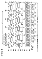
- Fig. 1 denotes a p-type semiconductor substrate.
- Reference numerals 2a to 2d, 3a to 3d, 4a to 4d and 5a to 5d respectively represent four photosensitive picture elements, for example, photodiodes arranged in the direction of a column.
- Reference numerals 6a to 6d show columnar shift registers respectively set adjacent to each columnar group of photosensitive picture elements.
- Reference numeral 7 denotes a row-directed shift register extending in a row direction intersecting at right angles the column direction in which the columnar shift registers 6a to 6d are arranged.
- Reference numerals 8a to 8d indicate overflow control electrodes which are positioned on the opposite side of the respective columnar groups of photosensitive picture elements to the columnar groups of shift registers 6a to 6d.
- Overflow drains 9a to 9d of n + regions are provided on the left side of the respective overflow control electrodes 8a to 8d.
- Reference numeral 10 is a charge output terminal of the aforesaid shift register 7 extending in the row direction.
- the photosensitive picture elements 2a to 2d, 3a to 3d, 4a to 4d, 5a to 5d of the conventional area image sensor receive a light for a prescribed length of time, then a signal charge is generated in each of the photosensitive picture elements in an amount corresponding to the luminosity of the light received.
- the signal charges are transferred to the corresponding shift registers 6a to 6d, and thereafter sent forth from the output terminal 10 through the row-extending shift register 7. Excess charges produced in the picture elements due to the projection of a light having a greater luminosity than prescribed run beyond potential barriers formed in those portions of the semiconductor substrate 1 which lie below the overflow control electrodes 8a to 8d set at a prescribed level of potential, and then flow into the overflow drains 9a to 9d. Therefore, excess charges generated in the picture elements are eliminated, thereby suppressing the occurrence of blooming.
- the conventional area image sensor is accompanied with the following drawbacks.
- overflow control electrodes and overflow drains have to be provided for the respective columnar groups of photosensitive picture elements, failing to increase the integration density of photosensitive picture elements, and consequently presenting difficulties in improving the resolving power of displayed images.
- excess charges generated in the picture elements are conducted to the corresponding overflow drains, thereby indeed suppressing the occurrence of blooming which might otherwise arise from such excess charges.
- this invention provides a charge transfer type area image sensor which comprises: a photosensitive section which is constructed by arranging a plurality of photosensitive picture elements for storing a signal charge generated in accordance with the intensity of an incoming light on a semiconductor substrate of a first conductivity type in the direction of the column and the direction of the row to make a two-dimensional form; a plurality of columnar shift registers which include charge transfer channels disposed in parallel with the columnar groups of the photosensitive picture elements of the photosensitive section and a plurality of charge transfer electrodes mounted on the charge transfer channels with an insulation layer interposed therebetween, thereby transferring a charge in a prescribed direction; first means for sequentially selecting the row groups of the photosensitive picture elements of the photosensitive section in response to a first selection signal, transmitting the signal charges stored in the selected row group of the picture elements to the corresponding columnar shift register and further conducting the transmitted signal charge in the prescribed direction; second means disposed adjacent to the last charge transfer electrode of the respective columnar groups of shift registers
- drive voltages or pulse trains respectively including pulses having voltage levels Vl, V2, V3, V4 are impressed on the charge transfer electrodes corresponding to the respective photosensitive picture elements.
- the semiconductor substrate is of the p conductivity type
- the above mentioned voltage levels retain the following relationship: A signal charge stored in a photosensitive picture element corresponding to the signal charge transfer electrode on which a pulse having a voltage level of V4 is impressed is transmitted to the charge transfer channel of the corresponding columnar group of shift registers. An excess charge stored in a photosensitive picture element corresponding to the charge transfer electrode on which a pulse having a voltage level of V3 is impressed is transmitted to the charge transfer channel of the corresponding columnar group of shift registers.
- a charge transfer electrode is impressed with a pulse having a voltage level of V2
- a signal charge and excess charge transmitted to the charge transfer channel are transferred to the prescribed side of the columnar groups of shift registers.
- the voltage level on the charge transfer electrode is so controlled by a pulse having a voltage level of Vl as to cause a potential barrier to be produced between a potential well for effecting the transfer of the signal charge and a potential well for carrying out the transfer of the excess charge.
- the gate of the control electrode remains closed, thereby causing a signal charge to be temporarily stored in an area defined below the storage electrode of the second means.
- the temporarily stored signal charge is sent forth from the output terminal of the row-directed shift register for each row group of photosensitive picture elements.
- a plurality of columnar groups of shift registers have only to be arranged in parallel with the columnar groups of photosensitive picture elements, making it unnecessary to provide an overflow control electrode 8a and overflow drain 9a, as shown in Fig. 1 indicating the arrangement of the prior art area image sensor, for example, for the columnar group of photosensitive picture elements 2a to 2d.
- This arrangement elevates the integration density of photosensitive picture elements and improves the quality of a displayed picture. Further, excess charges generated in the respective photosensitive picture elements are drained off through a control gate, when transmitted to the last charge transfer electrode of the respective columnar groups of shift registers, thereby suppressing the occurrence of blooming which might otherwise arise from the excess charges.
- Fig. 2A is a plan view of a charge transfer type area image sensor of the interline system embodying this invention.
- Fig. 2B is a cross sectional view on line 2B-2B of Fig. 2A.
- Fig. 2C is a cross sectional view on line 2C-2C of Fig. 2A.
- Fig. 2D is a cross sectional view on line 2D-2D of Fig. 2A.
- Fig. 2E is a cross sectional view on line 2E-2E of Fig. 2A.
- Fig. 2F is a cross sectional view on line 2F-2F of Fig. 2A. Referring to Fig.
- reference numerals 12a to 12d, 13a to 13d, 14a to 14d, 15a to 15d denote the first, second, third and fourth columnar groups of n-type semiconductor island regions formed on a semiconductor substrate 11. These island regions, together with the semiconductor substrate 11, constitute photodiodes acting as photosensitive elements or picture elements.
- Four columnar groups of shift registers 21, 22, 23, 24 are arranged closely in parallel with the first to the fourth columnar groups of photosensitive picture elements.
- Each of the four columnar groups of shift registers 21, 22, 23, 24 comprises an n-type charge transfer channel 41 (Fig. 2B) embedded in the semiconductor substrate 11 and a plurality of charge transfer electrodes 16, 17, 18, 19 mounted on the charge transfer channel 41 with an insulation layer 45 interposed therebetween.
- the charge transfer electrodes 16, 17, 18, 19 correspond to the related photosensitive picture elements. However, the charge transfer electrode 20 does not directly correspond to any photosensitive picture element.
- reference numerals 12d, 13d, 14d, 15d are taken to denote a first row group of photosensitive elements.
- Reference numerals 12c, 13c, 14c, 15c are taken to represent a second row group of photosensitive elements.
- Reference numerals 12b, 13b, 14b, 15b are supposed to show a third row group of photosensitive elements.
- Reference numerals 12a, 13a, 14a, 15a are assumed to indicate a fourth row group of photosensitive elements.
- the charge transfer channels 41 of the respective columnar groups of shift registers extends to the later described row-directed shift register 40.
- the row-directed shift register 40 intersects the respective columnar groups of shift registers and is set adjacent to four bottom gates 27.
- the row-directed shift register 40 comprises signal charge transfer electrodes 31a, 31b, 32a, 32b, 33a, 33b, 34a, 34b, 35a, 35b, 36a, 36b, 37a, 37b, 38a, 38b arranged in the order mentioned as counted from the left side of Fig. 2A.
- Reference numeral 39a is an output terminal and reference numeral 39 is an output stage of the shift register 40.
- a control gate 28 is provided adjacent to the last charge transfer electrode 20 of the respective columnar groups 21, 22, 23, 24 of shift registers. As shown in Fig. 2E, n + semiconductor island regions 29, namely, drains are formed on the semiconductor substrate 11 adjacent to the corresponding control gates 28.
- the subject area image sensor further comprises a drive circuit 30 for issuing drive pulse trains ⁇ 1 to ⁇ 7 and ⁇ d.
- the pulse train ⁇ 1 is supplied to the charge transfer electrode groups 16 corresponding to the fourth row group of photosensitive picture elements.
- the pulse train ⁇ 2 is conducted to the charge transfer electrodes 17 corresponding to the third row group of photosensitive picture elements.
- the pulse train ⁇ 3 is delivered to the charge transfer electrodes 18 corresponding to the second row group of photosensitive picture elements.
- the pulse train ⁇ 4 is supplied to the charge transfer electrodes 19 corresponding to the first row group of photosensitive picture elements.
- the pulse train ⁇ 5 is delivered to the last charge transfer electrode 20 of the respective columnar groups of photosensitive picture elements.
- the pulse train ⁇ 6 is sent to the storage electrode groups 25, 26.
- the pulse train ⁇ 7 is carried to the bottom gate group 27.
- the pulse train $d is supplied to the control gate group 28. Further, positive high voltage V D is impressed on the drain group 29.
- a clock pulse ⁇ rl is supplied to the signal charge transfer electrodes 32a, 32b, 34a, 34b, 36a, 36b, 38a, 38b of the row-directed shift register 40.
- a clock pulse ⁇ r2 is impressed on the signal charge transfer electrodes 31a, 31b, 33a, 33b, 35a, 35b, 37a, 37b of the row-directed shift register 40.
- n-type semiconductor regions 41 for providing charge transfer channel for the columnar groups 21 to 24 of shift registers are formed on the surface of the semiconductor substrate 11 in a state extending to the signal charge transfer channel of the row-directed shift register 40.
- n-type charge transfer channel 41 Mounted on the n-type charge transfer channel 41 are charge transfer electrodes 16, 17, 18, 19, the last charge transfer electrode 20 of the respective columnar groups of shift registers, storage electrodes 25, 26, bottom gate 27 and the signal charge transfer electrode 32a of the row-directed shift register 40 in the order mentioned as counted from the left side of Fig. 2B, with an insulation layer 45 interposed between the n-type semiconductor region 41 and all the above-mentioned electrodes.
- a p-type semiconductor island region 42 is formed on those portions of the surface of the n-type charge transfer channel 41 which face the storage electrode 25 and bottom gate 27 in order to act as a potential barrier for defining the direction in which the charge is transferred, that is, for preventing the backward flow of the signal charge.
- a control electrode 28 is mounted on the charge transfer electrode 20 with an insulation layer 45 interposed therebetween.
- Reference numeral 43 of Fig. 2B is a p-type channel stop region.
- An optical shield 44 is formed on the respective electrodes with an insulation layer interposed therebetween.
- the portion 46d of the surface of the semiconductor substrate 11 is exposed between an n-type region constituting a picture element 12d and an n-type charge transfer channel 41 of the columnar group 21 of shift registers.
- a charge transfer electrode 19 is formed above the exposed portion 46d of the semiconductor substrate 11 and charge transfer channel 41 with the insulation layer 45 interposed therebetween.
- a potential barrier formed on the exposed portion 46d of the semiconductor substrate 11 has its height controlled in accordance with the level of voltage impressed on the charge transfer electrode 19.
- FIG. 2E indicates the relative positions of the n-type charge transfer channel 41, drain 29, control gate 28 and charge transfer electrode 20 of the columnar groups 21, 22 of shift registers.
- the elements 41, 29, 28, 20 of the other columnar groups 23, 24 of shift registers have the same relative positions.
- the parts of Figs. 2D and 2F the same as those of Figs. 2B, 2C, 2E are denoted by the same numerals, description thereof being omitted.
- Fig. 3 is a timing chart showing the waveforms of pulse trains ⁇ 1 to ⁇ 7 and ⁇ d issued from the drive circuit 30 of Fig. 2A and clock pulses ⁇ r1, ⁇ r2 applied to the row-directed shift register 40 and an output signal of the row-directed shift register 40.
- the pulse trains ⁇ 1 to ⁇ 4 respectively have voltage levels V1 (used as the reference), V2, V3, V4. These voltage levels have the following relationship:
- a pulse having a voltage level of V4 is referred to as a first selection signal.
- a pulse having a voltage level of V3 is referred to as a second selection signal.
- a pulse having a voltage level of V2 is assumed to be used for transmission of a charge.
- the pulse train ⁇ 5 has voltage levels V3, V2.
- Pulse trains ⁇ d, ⁇ 6, ⁇ 7, clock pulses ⁇ r1, ⁇ r2 respectively have high and low voltage levels V H , V L .
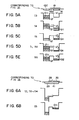
- Figs. 4A to 4P indicate the relationship between potential wells formed in the respective regions extending from the columnar group of shift registers 21 to the row-directed shift register 40 and the corresponding charges.
- Figs. 5A to 5E indicate the relationship between a charge stored in the picture element 12d of Fig. 2C and a charge stored in a potential well formed below the charge transfer electrode 19, and also the relationship between the charge and the height of the potential barrier formed at the exposed portion 46d of the semiconductor substrate.
- Figs. 6A and 6B indicate the manner in which excess charges are expelled to the drain 29 shown in Fig. 2E.
- a charge transfer type area image sensor of Fig. 2A embodying this invention with reference to Figs. 3, 4A to 4P, 5A to 5E and 6A, 6B.
- a signal charge Q14 generated in the photosensitive picture element 12a of the fourth row of the first column is stored in a potential well formed below the storage electrode 26 during an (n-l)th frame preceding a nth frame by one frame Tf.
- a pulse train ⁇ 4 supplied to the charge transfer electrode 19 of the shift register 21 which faces the picture element 12d of the first row of the first column has the same voltage level as the voltage level V3 of the second selection signal.
- a potential barrier formed on the surface of the exposed portion 46d (Fig. 2C) of the semiconductor substrate 11 which faces the picture element 12d has a potential barrier of V3' (Fig. 5D).
- the excess charge Qe runs over the potential barrier V3' into a potential well formed below the charge transfer electrode 19 (Fig. 5 D ).
- Fig. 4A indicates the excess charge Qe running into a potential well formed below the charge transfer electrode 19.
- a pulse train ⁇ 5 supplied to the charge transfer electrode 20 has the same voltage level as the voltage level V3 of the second selection signal and a pulse train ⁇ d delivered to the control gate 28 has a high voltage level V H . Therefore, the charge transfer electrode 20 and a potential well formed below the control gate 28 have a voltage level indicated in Fig. 6A, causing the excess charge Qe produced in the picture element 12d to run below the control gate 28 and be drawn off to the drain 29.
- pulses trains ⁇ 1, ⁇ 4 have a low voltage level of VI alike. Consequently, potential barriers formed on the surfaces of the exposed portions 46a, 46d which respectively face the picture elements 12a, 12d have a high potential barrier Vl' (Fig. 5A), causing a signal charge Qll to be stored in the picture element 12d of the first row of the first column (Fig. 5A).
- a pulse train $7 supplied to the bottom gate 27 still stands at a low voltage level V L , causing a signal charge Q14 shown in Fig. 4A to remain stored in a potential well formed below the storage electrode 26 (Fig. 4C).
- a pulse train ⁇ 4 supplied to the charge transfer electrode 19 has the same voltage level as the voltage level V4 of the first selection signal. Therefore, the signal charge Qll (Fig. 5A) stored in the picture element 12d of the first row of the first column is transmitted to the charge transfer channel 41 of the columnar group 21 of shift registers, namely, to a potential well formed below the charge transfer electrode 19 (Fig. 5B).
- a charge Qr shown in Fig. 5C is a residual charge remaining in the picture element 12d after the transmission of the signal charge Q11.
- the bottom gate 27 is opened, and a signal charge Q14 (Figs.
- pulse trains $4, $5 supplied to the charge transfer electrodes 19, 20 have the same voltage level alike as the level V2 of a charge transfer voltage.
- a potential barrier formed on the surface of the exposed portion 46d ⁇ Fig. 2C) of the semiconductor substrate 11 which faces the picture element 12d of the first row of the first columnar group 21 of shift registers has a high voltage level V2' (Fig. 5C). Since, at this time, a pulse train ⁇ d has a low voltage level V L , the control gate 28 remains closed. Therefore, a signal charge Qll generated in the picture element 12d is stored in a potential well formed in an area extending over the underside of the charge transfer electrodes 19, 20 of the first columnar group 21 of shift registers (Fig.
- a pulse train $6 supplied to the storage electrodes 25, 26 has a high voltage level Vg. Therefore, a signal charge Qll (Fig. 4E) generated in the picture element 12d and later stored in a potential well formed in an area extending over the underside of two charge transfer electrodes 19, 20 is transmitted to a potential well formed below the storage electrodes 26, 27 (Fig. 4F).
- a pulse train ⁇ 2 delivered to the charge transfer electrode 17, and a pulse train ⁇ 1 have the same voltage level alike as the voltage level V3 of the second selection signal. Therefore, an excess charges Qe generated in the picture elements 12a, 12b are respectively transmitted to potential wells formed below the corresponding charge transfer electrodes 16, 17 (Fig. 4F).
- pulse trains ⁇ 1 to ⁇ 5 are successively made to have the same voltage level as the voltage level V3 of the second selection signal. Therefore, excess charges Qe generated in the picture elements 12a to 12d of the first columnar group are transmitted to the charge transfer channel 41 of the first columnar group 21 of shift registers and then to a potential well formed below the charge transfer electrode 20. During a period which extends from a point of time t5 to a point of time t13, a charge generated in the semiconductor substrate 11 is conducted to the charge transfer channel 41.
- the above-mentioned excess charges Qe transmitted to the potential well formed below the charge transfer electrode 20 have a magnitude equal to a sum of the signal charges generated in the aforementioned picture elements 12a to 12d of the first columnar group and a charge produced in the semiconductor substrate 11.
- a pulse train ⁇ 3 supplied to the charge transfer electrode 18 has the same voltage level as the voltage level V4 of the first selection signal. Therefore, the signal charges stored in the picture elements 12c, 13c, 14c, 15c of the second row of the first to the fourth columnar groups are respectively transferred to the potential wells formed below the charge transfer electrodes of the corresponding columnar groups 21, 22, 23, 24 of shift registers.
- Fig. 4N indicates a signal charge Q12 which was stored in the picture element 12c of the second row of the first column and then transmitted to a potential well formed below the charge transfer electrode 18.
- a pulse train ⁇ 7 supplied to the bottom gate 27 has a high voltage level V H , causing the bottom gate 27 to remain open.
- a signal charge Qll (Fig. 4M) stored in the picture element 12d of the first row of the first column is conducted below the bottom gate 27 to a potential well formed below the signal charge transfer electrode 32a of the row-directed shift register 40 (Fig. 4N). Further at the point of time t14, the signal charges which were generated in the picture elements 13d, 14d, 15d of the first row of the second to the fourth columnar groups and then transmitted to the storage electrodes 26 of the columnar groups of picture elements are simultaneously delivered to the row-directed shift register 40.
- pulse trains ⁇ 3, ⁇ 4 supplied to the charge transfer electrodes 18, 19 have the same voltage level as the charge transfer voltage V2.
- a signal charge Q12 generated in the picture element 12c is transmitted to a potential well formed in an area extending over the underside of two charge transfer electrodes 18, 19 (Fig. 4P).
- This signal charge Q12 is temporarily stored in a potential well formed below the storage electrode 26. While the signal charge Q12 is kept stored in a potential well formed below the storage electrode 26, the excess charges Qe generated in the picture elements are successively conducted below the charge transfer electrodes 16 to 20 to the drains 29.
- signal charges stored in the picture elements 12c, 13c, 14c, 15c of the second row of the first to the fourth columnar groups are transmitted to the row-directed shift register 40, which sends forth signal charges 12c', 13c', 14c', 15c' in succession.
- signal charges stored in the picture elements 12b, 13b, 14b, 15b of the third row of the first to the fourth columnar groups are transmitted to the row-directed shift register 40.
- signal charges stored in the picture elements 12a, 13a, 14a, 15a of the fourth row of the first to the fourth columnar groups are also transmitted to the row-directed shift register 40.
- signal charges 12b', 13b!, 14b', 15b', 12a', 13a', 14a', 15a' are successively sent forth from the output stage 39 of the subject area image sensor in synchronization with clock pulses ⁇ r1, ⁇ r2.
- a picture element 12d When control is made of the height of a potential barrier formed on the surface of the exposed portion 46d of the semiconductor substrate 11 which is defined between the picture element 12d and the charge transfer channel 41 of the first columnar group 21 of shift registers (Fig. 2C), then a signal charge and excess charge generated in the picture element 12d are separately transmitted to the corresponding columnar group of 21 of the shift registers. Both signal charge and excess charge are separately conducted along the charge transfer channel 41. The signal charge is temporarily stored in a potential well formed below the storage electrode 26. On the other hand, the excess charge is expelled to the drain 29 through the control gate 28.
- the charge transfer electrode 19 corresponding to the picture element 12d is supplied with a pulse train ⁇ 4 having a voltage level of V4 as a first selection signal, then a potential barrier formed on the surface of the exposed portion 46d of the semiconductor substrate 11 has its height reduced to a level of V4', causing a signal charge Qll to be transmitted to the charge transfer channel 41 (Fig. 5B).
- a pulse train ⁇ 4 supplied to the corresponding signal transfer electrode 19 has the same voltage level as the voltage level V3 of the second selection signal.
- the potential barrier formed on the surface of the exposed portion 46d of the semiconductor substrate 11 assumes a level of V3' higher than V4' (Fig. 5D). Consequently, a signal charge can be stored in the picture element 12d, until the potential barrier retains a height of V3'.
- a charge generated in the picture element 12d with a higher potential level than V3' is transmitted as an excess charge Qe to the charge transfer channel 41 (Fig. 5D). Where the signal charge and excess charge Qe are separately conducted by potential wells having different potential levels, then it is necessary to prevent the excess charge Qe from entering that potential well by which the signal charge is transmitted.
- an area image sensor embodying this invention is so arranged that a pulse train ⁇ 4 is issued with a voltage level of V2 for a prescribed period in order to enable a charge transfer electrode to be impressed with a voltage V1 lower than the aforementioned voltage level of V2, thereby forming a potential barrier between a potential well by which a signal charge is transmitted and a potential well by which an excess charge is conducted.
- a pulse train ⁇ 4 is issued with a voltage level of V2 for a prescribed period in order to enable a charge transfer electrode to be impressed with a voltage V1 lower than the aforementioned voltage level of V2, thereby forming a potential barrier between a potential well by which a signal charge is transmitted and a potential well by which an excess charge is conducted.
- a saturated luminosity IM of a light projected on each picture element is indicated as Q M/ K.Tf (where C denotes a static capacity prevailing between the semiconductor substrate 11 and n-type semiconductor island regions 12a to 12d, 13a to 13d, 14a to 14d, 15a to 15d; Tf represents one frame period (Fig. 3); and K is a constant of light-signal conversion occurring in a picture element).
- a maximum luminosity I BM of a light projected on a picture element is set at C.(V3'-V2')/2K.Tr in order to suppress the occurrence of blooming.
- the area image sensor of this invention shown in Fig. 2A which eliminates the necessity of providing, for example, an overflow electrode 9a and overflow control electrode 8a close to the respective columnar groups of photosensitive picture elements as in the prior art image sensor of Fig. 1 can elevate the integration density of photosensitive picture elements as previously mentioned. With the chip taken to have the same size, this invention can more prominently improve the resolving capacity, and further more noticeably decrease the occurrence of smearing resulting from charges generated particularly in the semiconductor substrate than has been possible with the prior art area image sensor. The reason for this runs as follows.
- Q SB represents the total quantity of charge which are generated in the semiconductor substrate 11 and then brought into the charge transfer channels 41 of the columnar groups of shift register during one frame Tf.
- signal charges are issued 16 times during one frame Tf from the row-directed shift register 7. Therefore, a smear component included in a signal charge issued each time, that is, an average quantity of excess charges generated in the semiconductor substrate 11 is expressed as Qgg/16.
- smear components are only composed of charges transmitted from the semiconductor substrate 11 into a potential well formed below the charge transfer electrode which transmits a signal charge when impressed with a signal transfer voltage of V2.
- Fig. 7 indicates the arrangement of that section of the drive circuit 30 of Fig. 2A which issues pulse trains ⁇ 1 to ⁇ 5.
- Fig. 8 is a timing chart of signals supplied to the circuit of Fig. 7.
- reference numeral 51 denotes a shift register for successively shifting an input signal Dl in synchronization with a clock pule ⁇ c.
- Reference numeral 52 represents a shift register for successively shifting an input signal D2 in synchronization with the clock pulse ⁇ c.
- Reference numerals 53, 54 show paired MOS transistors whose sources are connected together to send forth a pulse train ⁇ 1.
- the drain of the MOS transistor 53 is supplied with a signal A o and the drain of the MOS transistor 54 is impressed with a reference voltage VO (VO ⁇ Vl in Fig. 3).
- the gate of the MOS transistor 53 is supplied with a first output signal from the shift register 51.
- the gate of the MOS transistor 54 is supplied with a first output signal from the shift register 52.
- Groups of reference numerals 55-56, 57-58, 59-60 and 61-62 represent a plurality of pairs of MOS transistors which are connected together in a manner similar to that in which the first mentioned group of paired MOS transistors 53, 54 are coupled together.
- the above-mentioned groups of MOS transistors are only indicated, description thereof being omitted.
- Pulses trains ⁇ 2, ⁇ 3, ⁇ 4, ⁇ 5 are sent forth from the drains of the other MOS transistor pairs 55-56, 57-58, 59-60 and 61-62.
- An input signal A o has a voltage level V5 (V5 ⁇ V2 in Fig. 3).
- An input signal A E has a voltage level V6 (V6 > V4 in Fig. 3).
- the high voltage level of a signal Dl and the low voltage level of a signal D2 are changed in the timing indicated in Fig. 8.
- the sources of the respective MOS transistor pairs are impressed with the voltage level of V3 of the second selection signal through the corresponding resistors 63, 64, 65, 66, 67. Referring to Fig.
- an input signal Dl to the shift register 51 is successively shifted for each period T of a clock pulse ⁇ c, thereby rendering MOS transistors 53, 55, 57, 59, 61 conducting in turn.
- An input signal D2 to the shift register 52 is successively shifted for each period T of a clock pulse ⁇ c, thereby rendering MOS transistors 54, 56, 58, 60, 62 conducting in turn.
- output pulse trains ⁇ 1 to ⁇ 5 respectively have a voltage level of V3.
- output pulse trains ⁇ 1 to $5 have a voltage level of V2 obtained by dividing voltage difference between the voltages of V5 and V3 by the internal resistance of the MOS transistors 53, 55, 57, 59, 61 rendered conducting and the resistors 63, 64, 65, 66, 67 corresponding to the MOS transistors 53, 55, 57, 59, 61.
- the pulse trains ⁇ 1 to ⁇ 5 have a voltage level of V1 obtained by dividing voltage difference between the voltages of VO and V3 by the internal resistance of the MOS transistors 54, 56, 58, 60, 62 rendered conducting and the corresponding resistors 63, 64, 65, 66, 67.
- the pulse trains ⁇ 1 to ⁇ 4 have a voltage level of V4.
- the pulse trains ⁇ 1 to ⁇ 5 of Fig. 3 have their voltage levels defined as described above.
- I BM and I M have substantially the same relationship as is realized when an overflow drain 9a is provided as shown in Fig. 1.
- smear components resulting from charges generated in the semiconductor substrate 11 are expressed as Q SB/ M.N per picture element.
- the smear components are far more reduced to a value approximately expressed as 2Q S g/M 2 N.
- smear components occurring in the area image sensor of this invention are prominently reduced to 1/250 of the quantity of smear components arising in the conventional area image sensor. Therefore, the larger the number of photosensitive picture elements, the more effective the suppression of the blooming and smear is carried out by the present invention.
- the photodiode used as a photosensitive picture element can be replaced by a picture element which comprises a transparent electrode mounted on a semiconductor substrate with an insulation layer interposed therebetween, and wherein use is made of a depletion region formed below the transparent electrode by impressing a voltage thereon or a picture element which comprises a signal charge-storing electrode positioned near a photodiode.
- the row-directed shift register actuated by clock pulses ⁇ r1, ⁇ r2 having different phases can be replaced by a drive system of the CCD type (charge coupled device) or BBD type (bucket brigade device) actuated by clock pulses of the single, 3 or 4 phases.
- the level of a threshold voltage of the exposed portions 46a to 46d of the semiconductor substrate 11 can be controlled by diffusing an impurity in the surface of the exposed portions 46a to 46d by ion implantation.
- a charge transfer channel in which an n-type semiconductor region 41 is embedded can be replaced by a surface channel type charge transfer channel.
- a circuit for issuing pulse trains ⁇ 1 to ⁇ 5 used with the drive circuit 30 is not limited to that which is arranged as shown in Fig. 7. Obviously the waveforms of the pulse trains ⁇ 1 to .7 and pulse train .d can be changed.
- the excess charge Qe can be transmitted, as shown in Fig. 10, by numerous independent potential wells formed below numerous signal transfer electrodes, instead of a common potential well, as shown in Fig. 9, formed below numerous charge transfer electrodes.
Landscapes
- Engineering & Computer Science (AREA)
- Physics & Mathematics (AREA)
- Power Engineering (AREA)
- General Physics & Mathematics (AREA)
- Electromagnetism (AREA)
- Condensed Matter Physics & Semiconductors (AREA)
- Computer Hardware Design (AREA)
- Microelectronics & Electronic Packaging (AREA)
- Signal Processing (AREA)
- Multimedia (AREA)
- Computer Vision & Pattern Recognition (AREA)
- Solid State Image Pick-Up Elements (AREA)
- Transforming Light Signals Into Electric Signals (AREA)
Abstract
Description
- This invention relates to a charge transfer type area image sensor, and more particularly to a charge transfer type area image sensor which assures an increase in the integration density of picture elements and the function of suppressing blooming.
- The charge transfer type area image sensor is used as an image device, for example, in an optical character recognition system (OCR) or television camera. A charge transfer type area image sensor known to date includes the frame transfer system and interline system. Both systems have to be provided with means for eliminating an excess charge stored in picture elements in order to suppress blooming resulting from an intense incoming light. For better understanding of this invention, description is now given with reference to Fig. 1 of the conventional charge transfer type area image sensor of the interline system.
Reference numeral 1 denotes a p-type semiconductor substrate. Reference numerals 2a to 2d, 3a to 3d, 4a to 4d and 5a to 5d respectively represent four photosensitive picture elements, for example, photodiodes arranged in the direction of a column.Reference numerals 6a to 6d show columnar shift registers respectively set adjacent to each columnar group of photosensitive picture elements.Reference numeral 7 denotes a row-directed shift register extending in a row direction intersecting at right angles the column direction in which the columnar shift registers 6a to 6d are arranged. Reference numerals 8a to 8d indicate overflow control electrodes which are positioned on the opposite side of the respective columnar groups of photosensitive picture elements to the columnar groups ofshift registers 6a to 6d. Overflow drains 9a to 9d of n+ regions are provided on the left side of the respective overflow control electrodes 8a to 8d.Reference numeral 10 is a charge output terminal of theaforesaid shift register 7 extending in the row direction. - Where the photosensitive picture elements 2a to 2d, 3a to 3d, 4a to 4d, 5a to 5d of the conventional area image sensor receive a light for a prescribed length of time, then a signal charge is generated in each of the photosensitive picture elements in an amount corresponding to the luminosity of the light received. The signal charges are transferred to the
corresponding shift registers 6a to 6d, and thereafter sent forth from theoutput terminal 10 through the row-extendingshift register 7. Excess charges produced in the picture elements due to the projection of a light having a greater luminosity than prescribed run beyond potential barriers formed in those portions of thesemiconductor substrate 1 which lie below the overflow control electrodes 8a to 8d set at a prescribed level of potential, and then flow into the overflow drains 9a to 9d. Therefore, excess charges generated in the picture elements are eliminated, thereby suppressing the occurrence of blooming. - However, the conventional area image sensor is accompanied with the following drawbacks. First, overflow control electrodes and overflow drains have to be provided for the respective columnar groups of photosensitive picture elements, failing to increase the integration density of photosensitive picture elements, and consequently presenting difficulties in improving the resolving power of displayed images. In the second place, excess charges generated in the picture elements are conducted to the corresponding overflow drains, thereby indeed suppressing the occurrence of blooming which might otherwise arise from such excess charges. But the prior art area image sensor is still accompanied with the difficulties that excess charges from other sources, that is, those produced in the
semiconductor substrate 1 are partly diverted into the columnar groups ofshift registers 6a to 6d; where, in such case, an intense spot light is received, then excess charges generated in thesemiconductor substrate 1 leak to theshift registers 6a to fid; and consequently vertically extending white lines appear on a displayed image. Those white lines are referred to as a smear phenomenon (a kind of blooming) which prominently degrades the quality of a displayed image. - It is accordingly the object of this invention to provide a charge transfer type area image sensor whose image-resolving power is improved by elevating the integration degree of picture elements and which minimizes the occurrence of blooming resulting from excess charges produced in the semiconductor substrate.
- To attain the above-mentioned object, this invention provides a charge transfer type area image sensor which comprises: a photosensitive section which is constructed by arranging a plurality of photosensitive picture elements for storing a signal charge generated in accordance with the intensity of an incoming light on a semiconductor substrate of a first conductivity type in the direction of the column and the direction of the row to make a two-dimensional form; a plurality of columnar shift registers which include charge transfer channels disposed in parallel with the columnar groups of the photosensitive picture elements of the photosensitive section and a plurality of charge transfer electrodes mounted on the charge transfer channels with an insulation layer interposed therebetween, thereby transferring a charge in a prescribed direction; first means for sequentially selecting the row groups of the photosensitive picture elements of the photosensitive section in response to a first selection signal, transmitting the signal charges stored in the selected row group of the picture elements to the corresponding columnar shift register and further conducting the transmitted signal charge in the prescribed direction; second means disposed adjacent to the last charge transfer electrode of the respective columnar groups of shift registers and provided with charge storage means for temporarily storing the signal charge transmitted by the first means; third means for selecting at least once all the row groups of photosensitive picture elements in response to a second selection signal during a period extending from a point of time at which the first means selects a prescribed row group of photosensitive picture elements to a point of time at which the first means selects a succeeding row group of photosensitive picture elements, transmitting excess charges stored in the respective picture elements to the corresponding columnar groups of shift registers, and conducting the transmitted excess charges in the prescribed direction; fourth means which comprises a control electrode positioned adjacent to the last charge transfer electrode of the respective columnar groups of shift registers and a drain region disposed adjacent to the control electrode, and discharges the excess charge transmitted by the third means to the drain region by controlling the level of a voltage impressed on the control electrode; and a row-directed register for converting signal charges of the respective row groups of photosensitive picture elements temporarily stored by the second means into series signal charges and sending forth the series signal charges in the order of the row groups of photosensitive picture elements.
- With a charge transfer type area image sensor embodying this invention, drive voltages or pulse trains respectively including pulses having voltage levels Vl, V2, V3, V4 are impressed on the charge transfer electrodes corresponding to the respective photosensitive picture elements. Where the semiconductor substrate is of the p conductivity type, the above mentioned voltage levels retain the following relationship:

- With a charge transfer type area image sensor embodying this invention, a plurality of columnar groups of shift registers have only to be arranged in parallel with the columnar groups of photosensitive picture elements, making it unnecessary to provide an overflow control electrode 8a and overflow drain 9a, as shown in Fig. 1 indicating the arrangement of the prior art area image sensor, for example, for the columnar group of photosensitive picture elements 2a to 2d. This arrangement elevates the integration density of photosensitive picture elements and improves the quality of a displayed picture. Further, excess charges generated in the respective photosensitive picture elements are drained off through a control gate, when transmitted to the last charge transfer electrode of the respective columnar groups of shift registers, thereby suppressing the occurrence of blooming which might otherwise arise from the excess charges. Like these excess charges, those portions of the charges generated in the semiconductor substrate which leak to the potential well for effecting the transfer of excess charges produced in the columnar groups of charge transfer channels are drained off when conducted to an area defined below the last charge transfer electrode of the respective columnar groups of shift registers, thereby reducing the occurrence of the aforementioned smears. In contrast, with the conventional area image sensor arranged in Fig. 1, the above-mentioned leak current never fail to be transmitted to the row groups shift registers.
- This invention can be more fully understood from the following detailed description when taken in conjunction with the accompanying drawings, in which:
- Fig. 1 is a plan view of the conventional charge transfer type area'image sensor of the interline system;
- Fig. 2A is a plan view of a charge transfer type area image sensor of the interline system embodying this invention;
- Fig. 2B is a cross sectional view on
line 2B-2B of Fig. 2A; - Fig. 2C is a cross sectional view on
line 2C-2C of Fig. 2A; - Fig. 2D is a cross sectional view on
line 2D-2D of Fig. 2A; - Fig. 2E is a cross sectional view on
line 2E-2E of Fig. 2A; - Fig. 2F is a cross sectional view on
line 2F-2F of Fig. 2A; - Fig. 3 is a timing chart showing the waveforms of pulse trains for driving the area image sensor of Fig. 2A;
- Figs. 4A to 4P are timing charts illustrating the operation of the area image sensor of this invention, also showing the relationship between the shapes of potential wells formed in the areas defined below the electrodes indicated in Fig. 2B and the charges;
- Figs. 5A to 5E are timing charts illustrating the operation of the area image sensor of the invention, also showing the relationship between the shapes of potential wells formed in the areas defined below the electrodes indicated in Fig. 2C and the charges;
- Figs. 6A and 6B are timing charts illustrating the operation of the area image sensor of the invention, also showing the relationship between the shapes of potential wells formed in the area defined below the electrode indicated in Fig. 2E;
- Fig. 7 is a block circuit diagram of the main part of a driving circuit used with the area image sensor of Fig. 2A;
- Fig. 8 is a timing chart of signals supplied to the driving circuit of Fig. 7;
- Fig. 9 sets forth the principle by which a modification of the columnar group of shift registers shown in Fig. 2A is actuated; and
- Fig. 10 indicates the principle by which another modification of the columnar group of shift registers shown in Fig. 2A is operated.
- Fig. 2A is a plan view of a charge transfer type area image sensor of the interline system embodying this invention. Fig. 2B is a cross sectional view on
line 2B-2B of Fig. 2A. Fig. 2C is a cross sectional view online 2C-2C of Fig. 2A. Fig. 2D is a cross sectional view online 2D-2D of Fig. 2A. Fig. 2E is a cross sectional view online 2E-2E of Fig. 2A. Fig. 2F is a cross sectional view online 2F-2F of Fig. 2A. Referring to Fig. 2A, reference numerals 12a to 12d, 13a to 13d, 14a to 14d, 15a to 15d denote the first, second, third and fourth columnar groups of n-type semiconductor island regions formed on asemiconductor substrate 11. These island regions, together with thesemiconductor substrate 11, constitute photodiodes acting as photosensitive elements or picture elements. Four columnar groups ofshift registers shift registers semiconductor substrate 11 and a plurality ofcharge transfer electrodes charge transfer channel 41 with aninsulation layer 45 interposed therebetween. Thecharge transfer electrodes charge transfer electrode 20 does not directly correspond to any photosensitive picture element. For convenience of description,reference numerals Reference numerals 12c, 13c, 14c, 15c are taken to represent a second row group of photosensitive elements.Reference numerals Reference numerals charge transfer channels 41 of the respective columnar groups of shift registers extends to the later described row-directedshift register 40. As viewed in the direction of the column,storage electrodes bottom gate 27 are made to follow the lastcharge transfer electrode 20 of the respective columnar groups of shift registers in the order mentioned. The row-directedshift register 40 intersects the respective columnar groups of shift registers and is set adjacent to fourbottom gates 27. The row-directedshift register 40 comprises signalcharge transfer electrodes Reference numeral 39a is an output terminal andreference numeral 39 is an output stage of theshift register 40. Acontrol gate 28 is provided adjacent to the lastcharge transfer electrode 20 of the respectivecolumnar groups semiconductor island regions 29, namely, drains are formed on thesemiconductor substrate 11 adjacent to thecorresponding control gates 28. - The subject area image sensor further comprises a
drive circuit 30 for issuing drive pulse trains φ1 to φ7 and φd. The pulse train φ1 is supplied to the chargetransfer electrode groups 16 corresponding to the fourth row group of photosensitive picture elements. The pulse train φ2 is conducted to thecharge transfer electrodes 17 corresponding to the third row group of photosensitive picture elements. The pulse train ‡3 is delivered to thecharge transfer electrodes 18 corresponding to the second row group of photosensitive picture elements. The pulse train φ4 is supplied to thecharge transfer electrodes 19 corresponding to the first row group of photosensitive picture elements. The pulse train φ5 is delivered to the lastcharge transfer electrode 20 of the respective columnar groups of photosensitive picture elements. The pulse train φ6 is sent to thestorage electrode groups bottom gate group 27. The pulse train $d is supplied to thecontrol gate group 28. Further, positive high voltage VD is impressed on thedrain group 29. A clock pulse φrl is supplied to the signalcharge transfer electrodes shift register 40. A clock pulse ¢r2 is impressed on the signalcharge transfer electrodes shift register 40. - Description is now given with reference to Figs. 2B to 2F of the relationship between the semiconductor regions and electrode groups including charge transfer electrodes which are formed on the
semiconductor substrate 11. Referring to Fig. 2B, n-type semiconductor regions 41 (hereinafter referred to as "charge transfer channels") for providing charge transfer channel for thecolumnar groups 21 to 24 of shift registers are formed on the surface of thesemiconductor substrate 11 in a state extending to the signal charge transfer channel of the row-directedshift register 40. Mounted on the n-typecharge transfer channel 41 arecharge transfer electrodes charge transfer electrode 20 of the respective columnar groups of shift registers,storage electrodes bottom gate 27 and the signalcharge transfer electrode 32a of the row-directedshift register 40 in the order mentioned as counted from the left side of Fig. 2B, with aninsulation layer 45 interposed between the n-type semiconductor region 41 and all the above-mentioned electrodes. A p-typesemiconductor island region 42 is formed on those portions of the surface of the n-typecharge transfer channel 41 which face thestorage electrode 25 andbottom gate 27 in order to act as a potential barrier for defining the direction in which the charge is transferred, that is, for preventing the backward flow of the signal charge. Acontrol electrode 28 is mounted on thecharge transfer electrode 20 with aninsulation layer 45 interposed therebetween.Reference numeral 43 of Fig. 2B is a p-type channel stop region. Anoptical shield 44 is formed on the respective electrodes with an insulation layer interposed therebetween. As shown in Fig. 2C, theportion 46d of the surface of thesemiconductor substrate 11 is exposed between an n-type region constituting apicture element 12d and an n-typecharge transfer channel 41 of thecolumnar group 21 of shift registers. Acharge transfer electrode 19 is formed above the exposedportion 46d of thesemiconductor substrate 11 andcharge transfer channel 41 with theinsulation layer 45 interposed therebetween. A potential barrier formed on the exposedportion 46d of thesemiconductor substrate 11 has its height controlled in accordance with the level of voltage impressed on thecharge transfer electrode 19. An exposedportion 46d is also formed between thepicture element 13d and thecharge transfer channel 41 of thecolumnar group 22 of shift registers. The above-mentioned description also applies to the other picture elements, though not shown. Fig. 2E indicates the relative positions of the n-typecharge transfer channel 41,drain 29,control gate 28 andcharge transfer electrode 20 of thecolumnar groups elements columnar groups - Fig. 3 is a timing chart showing the waveforms of pulse trains φ1 to φ7 and ‡d issued from the
drive circuit 30 of Fig. 2A and clock pulses φr1, φr2 applied to the row-directedshift register 40 and an output signal of the row-directedshift register 40. The pulse trains φ1 to φ4 respectively have voltage levels V1 (used as the reference), V2, V3, V4. These voltage levels have the following relationship:
- In case where the
semiconductor substrate 11 has a conductivity type n, then the above-mentioned voltage levels have the following relationship:
- With this invention, a pulse having a voltage level of V4 is referred to as a first selection signal. A pulse having a voltage level of V3 is referred to as a second selection signal. A pulse having a voltage level of V2 is assumed to be used for transmission of a charge. The pulse train φ5 has voltage levels V3, V2. Pulse trains ¢d, φ6, φ7, clock pulses ¢r1, φr2 respectively have high and low voltage levels VH, VL. Where a voltage having a level of V4 is impressed on the
charge transfer electrodes 16 to 19, then signal charges stored in the corresponding picture elements are transmitted to thecharge transfer channel 41 of the columnar groups of shift registers. Where a voltage having a level of V3 is impressed on thecharge transfer electrodes 16 to 19, then excess charges stored in the corresponding picture elements are transmitted to thecharge transfer channel 41. Where a voltage having a level of V2 is impressed on thecharge transfer electrodes 16 to 19, then signal charges and excess charges transmitted to thecharge transfer channel 41 are transmitted by potential wells having different potential. The timings in which pulse trains φ5, φd, φ6 reach the prescribed voltage levels are so defined that excess charges are drawn off to thedrain 29, and a signal charge received is temporarily stored under thestorage electrodes storage electrodes shift register 40. - Figs. 4A to 4P indicate the relationship between potential wells formed in the respective regions extending from the columnar group of
shift registers 21 to the row-directedshift register 40 and the corresponding charges. Figs. 5A to 5E indicate the relationship between a charge stored in thepicture element 12d of Fig. 2C and a charge stored in a potential well formed below thecharge transfer electrode 19, and also the relationship between the charge and the height of the potential barrier formed at the exposedportion 46d of the semiconductor substrate. Figs. 6A and 6B indicate the manner in which excess charges are expelled to thedrain 29 shown in Fig. 2E. - Description is now given of a charge transfer type area image sensor of Fig. 2A embodying this invention with reference to Figs. 3, 4A to 4P, 5A to 5E and 6A, 6B. Now let it be assumed that at a point of time tl of Fig. 3, a signal charge Q14 generated in the photosensitive picture element 12a of the fourth row of the first column is stored in a potential well formed below the
storage electrode 26 during an (n-l)th frame preceding a nth frame by one frame Tf. At a point of time tl, a pulse train ‡4 supplied to thecharge transfer electrode 19 of theshift register 21 which faces thepicture element 12d of the first row of the first column has the same voltage level as the voltage level V3 of the second selection signal. Therefore, a potential barrier formed on the surface of the exposedportion 46d (Fig. 2C) of thesemiconductor substrate 11 which faces thepicture element 12d has a potential barrier of V3' (Fig. 5D). Where an excess charge Qe is generated in thepicture element 12d receiving an extremely luminous light, then the excess charge Qe runs over the potential barrier V3' into a potential well formed below the charge transfer electrode 19 (Fig. 5D). Fig. 4A indicates the excess charge Qe running into a potential well formed below thecharge transfer electrode 19. - At a point of time t2, a pulse train φ5 supplied to the
charge transfer electrode 20 has the same voltage level as the voltage level V3 of the second selection signal and a pulse train φd delivered to thecontrol gate 28 has a high voltage level VH. Therefore, thecharge transfer electrode 20 and a potential well formed below thecontrol gate 28 have a voltage level indicated in Fig. 6A, causing the excess charge Qe produced in thepicture element 12d to run below thecontrol gate 28 and be drawn off to thedrain 29. - At a point of time t3, pulses trains φ1, φ4 have a low voltage level of VI alike. Consequently, potential barriers formed on the surfaces of the exposed
portions 46a, 46d which respectively face thepicture elements 12a, 12d have a high potential barrier Vl' (Fig. 5A), causing a signal charge Qll to be stored in thepicture element 12d of the first row of the first column (Fig. 5A). At a point of time t3, a pulse train $7 supplied to thebottom gate 27 still stands at a low voltage level VL, causing a signal charge Q14 shown in Fig. 4A to remain stored in a potential well formed below the storage electrode 26 (Fig. 4C). - At a point of time t4, a pulse train φ4 supplied to the
charge transfer electrode 19 has the same voltage level as the voltage level V4 of the first selection signal. Therefore, the signal charge Qll (Fig. 5A) stored in thepicture element 12d of the first row of the first column is transmitted to thecharge transfer channel 41 of thecolumnar group 21 of shift registers, namely, to a potential well formed below the charge transfer electrode 19 (Fig. 5B). A charge Qr shown in Fig. 5C is a residual charge remaining in thepicture element 12d after the transmission of the signal charge Q11. At the point of time t4, since a pulse train φ7 has a high voltage level VH, thebottom gate 27 is opened, and a signal charge Q14 (Figs. 4A, 4B, 4C) stored in the picture element 12a of the fourth row of the first column during the (n-l)th frame preceding the nth frame by one frame Tf passes below thebottom gate 27 and is transmitted to a potential well formed below the signalcharge transfer electrode 32a of the row-directed shift register 40 (Fig. 4D). At the point of time t4, signal charges stored in thepicture elements charge transfer electrodes 19 of the correspondingcolumnar groups 22 to 24 of shift registers. Signal charges stored in thepicture elements charge transfer electrodes 34a, 36a, 38a of the row-directedshift register 40. Therefore, successively sent forth from theoutput stage 39 of the row-directedshift register 40 are four charge signals 12a', 13a', 14a', 15a' transmitted from thepicture elements storage electrodes - At a point of time t5, pulse trains $4, $5 supplied to the
charge transfer electrodes portion 46d {Fig. 2C) of thesemiconductor substrate 11 which faces thepicture element 12d of the first row of thefirst columnar group 21 of shift registers has a high voltage level V2' (Fig. 5C). Since, at this time, a pulse train φd has a low voltage level VL, thecontrol gate 28 remains closed. Therefore, a signal charge Qll generated in thepicture element 12d is stored in a potential well formed in an area extending over the underside of thecharge transfer electrodes first columnar group 21 of shift registers (Fig. 4E). At the point of time t5, a pulse train φ1 conducted to thecharge transfer electrode 16 has the same voltage level as the voltage level V3 of the second selection signal. Therefore, an excess charge Qe generated in the picture element 12a is transmitted to a potential well formed below the charge transfer electrode 16 (Fig. 4E). - At a point of time t6, a pulse train $6 supplied to the
storage electrodes picture element 12d and later stored in a potential well formed in an area extending over the underside of twocharge transfer electrodes storage electrodes 26, 27 (Fig. 4F). At the point of time t6, a pulse train φ2 delivered to thecharge transfer electrode 17, and a pulse train φ1 have the same voltage level alike as the voltage level V3 of the second selection signal. Therefore, an excess charges Qe generated in thepicture elements 12a, 12b are respectively transmitted to potential wells formed below the correspondingcharge transfer electrodes 16, 17 (Fig. 4F). - Between time points t7 and t13, as shown in Fig. 3, pulse trains φ1 to φ5 are successively made to have the same voltage level as the voltage level V3 of the second selection signal. Therefore, excess charges Qe generated in the picture elements 12a to 12d of the first columnar group are transmitted to the
charge transfer channel 41 of thefirst columnar group 21 of shift registers and then to a potential well formed below thecharge transfer electrode 20. During a period which extends from a point of time t5 to a point of time t13, a charge generated in thesemiconductor substrate 11 is conducted to thecharge transfer channel 41. Actually, therefore, the above-mentioned excess charges Qe transmitted to the potential well formed below thecharge transfer electrode 20 have a magnitude equal to a sum of the signal charges generated in the aforementioned picture elements 12a to 12d of the first columnar group and a charge produced in thesemiconductor substrate 11. - At a point of time t14, a pulse train φ3 supplied to the
charge transfer electrode 18 has the same voltage level as the voltage level V4 of the first selection signal. Therefore, the signal charges stored in thepicture elements 12c, 13c, 14c, 15c of the second row of the first to the fourth columnar groups are respectively transferred to the potential wells formed below the charge transfer electrodes of the correspondingcolumnar groups charge transfer electrode 18. At the point of time t14, a pulse train φ7 supplied to thebottom gate 27 has a high voltage level VH, causing thebottom gate 27 to remain open. Therefore, a signal charge Qll (Fig. 4M) stored in thepicture element 12d of the first row of the first column is conducted below thebottom gate 27 to a potential well formed below the signalcharge transfer electrode 32a of the row-directed shift register 40 (Fig. 4N). Further at the point of time t14, the signal charges which were generated in thepicture elements storage electrodes 26 of the columnar groups of picture elements are simultaneously delivered to the row-directedshift register 40. At points of time after the point of time tl4, foursignal charges 12d', 13d', 14d', 15d' stored in thepicture elements shift register 40 in synchronization with clock pulses φr1, φr2. During a period which extends from the point of time t8 to the point of time t14, a pulse train φd supplied to thecontrol gates 28 of the respective columnar groups of picture elements has a high voltage level VH, causing thecontrol gates 28 to remain open. During a period which extends from a point of time t8 to a point of time t14, an excess charge Qe is conducted below thecontrol gates 28 to the drains 29 (Fig. 6A). - At a point of time t15, pulse trains φ3, φ4 supplied to the
charge transfer electrodes charge transfer electrodes 18, 19 (Fig. 4P). This signal charge Q12 is temporarily stored in a potential well formed below thestorage electrode 26. While the signal charge Q12 is kept stored in a potential well formed below thestorage electrode 26, the excess charges Qe generated in the picture elements are successively conducted below thecharge transfer electrodes 16 to 20 to thedrains 29. During a period extending from a point of time tl6 to a point of time tl7, signal charges stored in thepicture elements 12c, 13c, 14c, 15c of the second row of the first to the fourth columnar groups are transmitted to the row-directedshift register 40, which sends forth signal charges 12c', 13c', 14c', 15c' in succession. During a period extending from a point of time tl7 to a point of time t18, signal charges stored in thepicture elements shift register 40. During a period extending from a point of time tl8 to a point of time t19, signal charges stored in thepicture elements shift register 40. As a result, signal charges 12b', 13b!, 14b', 15b', 12a', 13a', 14a', 15a' are successively sent forth from theoutput stage 39 of the subject area image sensor in synchronization with clock pulses φr1, φr2. - The characteristics of this invention will become apparent from the foregoing description. Reference is now made to, for example, a
picture element 12d. When control is made of the height of a potential barrier formed on the surface of the exposedportion 46d of thesemiconductor substrate 11 which is defined between thepicture element 12d and thecharge transfer channel 41 of thefirst columnar group 21 of shift registers (Fig. 2C), then a signal charge and excess charge generated in thepicture element 12d are separately transmitted to the corresponding columnar group of 21 of the shift registers. Both signal charge and excess charge are separately conducted along thecharge transfer channel 41. The signal charge is temporarily stored in a potential well formed below thestorage electrode 26. On the other hand, the excess charge is expelled to thedrain 29 through thecontrol gate 28. To describe in greater detail, where thecharge transfer electrode 19 corresponding to thepicture element 12d is supplied with a pulse train φ4 having a voltage level of V4 as a first selection signal, then a potential barrier formed on the surface of the exposedportion 46d of thesemiconductor substrate 11 has its height reduced to a level of V4', causing a signal charge Qll to be transmitted to the charge transfer channel 41 (Fig. 5B). During the greater part of a period in which a signal charge is stored in thepicture element 12d, a pulse train φ4 supplied to the correspondingsignal transfer electrode 19 has the same voltage level as the voltage level V3 of the second selection signal. Therefore, the potential barrier formed on the surface of the exposedportion 46d of thesemiconductor substrate 11 assumes a level of V3' higher than V4' (Fig. 5D). Consequently, a signal charge can be stored in thepicture element 12d, until the potential barrier retains a height of V3'. A charge generated in thepicture element 12d with a higher potential level than V3' is transmitted as an excess charge Qe to the charge transfer channel 41 (Fig. 5D). Where the signal charge and excess charge Qe are separately conducted by potential wells having different potential levels, then it is necessary to prevent the excess charge Qe from entering that potential well by which the signal charge is transmitted. To meet this requirement, an area image sensor embodying this invention is so arranged that a pulse train φ4 is issued with a voltage level of V2 for a prescribed period in order to enable a charge transfer electrode to be impressed with a voltage V1 lower than the aforementioned voltage level of V2, thereby forming a potential barrier between a potential well by which a signal charge is transmitted and a potential well by which an excess charge is conducted. For better understanding of this invention, reference was made particularly to thepicture element 12d. Obviously, the foregoing description also applies to any other picture elements. As seen from the foregoing description, a maximum charge quantity QM which can be stored in each picture element is expressed as C'(V4'-V3'). A saturated luminosity IM of a light projected on each picture element is indicated as QM/K.Tf (where C denotes a static capacity prevailing between thesemiconductor substrate 11 and n-type semiconductor island regions 12a to 12d, 13a to 13d, 14a to 14d, 15a to 15d; Tf represents one frame period (Fig. 3); and K is a constant of light-signal conversion occurring in a picture element). Where the quantity of a signal charge generated in a picture element during a period Tr in which pulse trains φ1 to φ4 retain a voltage level V2 (that is, the one period of clock pulses φr1, φr2) exceeds a level of C.(V3'-V2'), then the excess charge runs into a potential well by which the signal charge is transmitted, undesirably resulting in the occurrence of a sort of blooming. A maximum luminosity IBM of a light projected on a picture element is set at C.(V3'-V2')/2K.Tr in order to suppress the occurrence of blooming. Assuming V3'-V2' = V4'-V3', and Tf = 20Tr, there results IBM = 10IM. In other words, even where a maximum luminosity IBM of a light projecting on a picture element is 10 times higher than the saturated light luminosity IM, the area image sensor of this invention can suppress the occurrence of smearing. - Detailed description is now given of the advantages of the area image sensor of Fig. 2A embodying the invention over that of the prior art shown in Fig. 1. The area image sensor of this invention shown in Fig. 2A which eliminates the necessity of providing, for example, an overflow electrode 9a and overflow control electrode 8a close to the respective columnar groups of photosensitive picture elements as in the prior art image sensor of Fig. 1 can elevate the integration density of photosensitive picture elements as previously mentioned. With the chip taken to have the same size, this invention can more prominently improve the resolving capacity, and further more noticeably decrease the occurrence of smearing resulting from charges generated particularly in the semiconductor substrate than has been possible with the prior art area image sensor. The reason for this runs as follows. Now let it be assumed that QSB represents the total quantity of charge which are generated in the
semiconductor substrate 11 and then brought into thecharge transfer channels 41 of the columnar groups of shift register during one frame Tf. With the conventional area image sensor of Fig. 1, signal charges are issued 16 times during one frame Tf from the row-directedshift register 7. Therefore, a smear component included in a signal charge issued each time, that is, an average quantity of excess charges generated in thesemiconductor substrate 11 is expressed as Qgg/16. In contrast, with the area image sensor of the invention shown in Fig. 2, smear components are only composed of charges transmitted from thesemiconductor substrate 11 into a potential well formed below the charge transfer electrode which transmits a signal charge when impressed with a signal transfer voltage of V2. On the other hand, charges conducted to a potential well formed below the transfer electrode which transmits a signal charge when impressed with a second selection signal having a voltage level of V3 are expelled to thedrains 29, and consequently do not constitute smear components. Therefore, smear components resulting from charges generated in thesemiconductor substrate 11 are measured approximately as (QSB/16) x (2Tr/5Tr) =Q SB/40. This means that smear components anticipated from the area image sensor of this invention only account for two-fifth of the smear components experienced with the conventional area image sensor of Fig. 1. - Fig. 7 indicates the arrangement of that section of the
drive circuit 30 of Fig. 2A which issues pulse trains φ1 to φ5. Fig. 8 is a timing chart of signals supplied to the circuit of Fig. 7. Referring to Fig. 7,reference numeral 51 denotes a shift register for successively shifting an input signal Dl in synchronization with a clock pule φc.Reference numeral 52 represents a shift register for successively shifting an input signal D2 in synchronization with the clock pulse φc.Reference numerals MOS transistor 53 is supplied with a signal Ao and the drain of theMOS transistor 54 is impressed with a reference voltage VO (VO < Vl in Fig. 3). The gate of theMOS transistor 53 is supplied with a first output signal from theshift register 51. The gate of theMOS transistor 54 is supplied with a first output signal from theshift register 52. Groups of reference numerals 55-56, 57-58, 59-60 and 61-62 represent a plurality of pairs of MOS transistors which are connected together in a manner similar to that in which the first mentioned group of pairedMOS transistors resistors shift register 51 is successively shifted for each period T of a clock pulse ¢c, thereby renderingMOS transistors shift register 52 is successively shifted for each period T of a clock pulse φc, thereby renderingMOS transistors MOS transistors counterpart MOS transistors MOS transistors resistors MOS transistors MOS transistors counterpart transistors MOS transistors resistors MOS transistors counterpart MOS transistors - Description is now given of the reason why the application of the area image sensor of this invention to a solid image sensor used with the standard TV image pickup system further suppresses the occurrence of blooming. Now let it be assumed that an N number of photosensitive picture elements are arranged in the direction of the row, and an M number of photosensitive picture elements are arranged in the direction of the column; and that a signal charge Qs stored in each photosensitive element is to be transmitted. Further let it be assumed, as shown in Fig. 9, that the signal charge Qs is transmitted by a potential well formed below two charge transfer electrodes a, b; charge transfer electrodes al, bl set before the charge transfer electrode a, and charge transfer electrodes a2, b2 positioned after the charge transfer electrode b are respectively impressed with a low voltage Vl, thereby forming
potential barriers 50 on both sides of a potential well by which the signal charge Qs is transmitted; and the other charge transfer electrodes than those described above are impressed with a high voltage V3, thereby forming a potential well by which the excess charge Qe is transmitted. The previously described expression C·(V4'-V3') representing a maximum charge quantity QM which can be stored in one picture element, and also the aforesaid expression QM/K.Tf denoting a saturatedluminosity 1M are assumed to be also applicable to the above-mentioned assumptions. Referring to Fig. 9, a maximum luminosity IBM of a light projected on a picture element should satisfy the following equation:
- in order to prevent an excess charge Qe from entering the potential well by which the signal charge Qs is transmitted. Now let it be assumed that the previously mentioned N number of photosensitive picture elements arranged in the direction of the row, and the aforesaid M number of photosensitive picture elements arranged in the direction of the column are about 500 alike. Then there approximately results the following equation:

- Assuming V3'-V2' = V4'-V3' as previously mentioned, IBM is expressed as (M.N.IM)/2. Assuming M = N = 500, there results

- The terms IBM and IM have substantially the same relationship as is realized when an overflow drain 9a is provided as shown in Fig. 1. With the prior art area image sensor of Fig. 1, smear components resulting from charges generated in the
semiconductor substrate 11 are expressed as QSB/M.N per picture element. In contrast, with the area image sensor of this invention, the smear components are far more reduced to a value approximately expressed as 2QSg/M2N. In other words, assuming M = N = 500, smear components occurring in the area image sensor of this invention are prominently reduced to 1/250 of the quantity of smear components arising in the conventional area image sensor. Therefore, the larger the number of photosensitive picture elements, the more effective the suppression of the blooming and smear is carried out by the present invention. - Obviously, this invention is not limited to the foregoing embodiment, but may be practised in various modifications. For instance, (1) it is possible to replace the p-
type semiconductor substrate 11 by an n-type semiconductor substrate. (2) the photodiode used as a photosensitive picture element can be replaced by a picture element which comprises a transparent electrode mounted on a semiconductor substrate with an insulation layer interposed therebetween, and wherein use is made of a depletion region formed below the transparent electrode by impressing a voltage thereon or a picture element which comprises a signal charge-storing electrode positioned near a photodiode. (3) the row-directed shift register actuated by clock pulses φr1, φr2 having different phases can be replaced by a drive system of the CCD type (charge coupled device) or BBD type (bucket brigade device) actuated by clock pulses of the single, 3 or 4 phases. (4) the level of a threshold voltage of the exposed portions 46a to 46d of thesemiconductor substrate 11 can be controlled by diffusing an impurity in the surface of the exposed portions 46a to 46d by ion implantation. (5) it is possible to mount a plurality of groups ofcharge electrodes columnar groups 21 to 24 of shift registers and temporarily store signal charges transmitted from plural row groups of the photosensitive picture elements. (6) a charge transfer channel in which an n-type semiconductor region 41 is embedded can be replaced by a surface channel type charge transfer channel. (7) a circuit for issuing pulse trains φ1 to φ5 used with thedrive circuit 30 is not limited to that which is arranged as shown in Fig. 7. Obviously the waveforms of the pulse trains φ1 to .7 and pulse train .d can be changed. (8) the excess charge Qe can be transmitted, as shown in Fig. 10, by numerous independent potential wells formed below numerous signal transfer electrodes, instead of a common potential well, as shown in Fig. 9, formed below numerous charge transfer electrodes.
Claims (7)
Applications Claiming Priority (2)
| Application Number | Priority Date | Filing Date | Title |
|---|---|---|---|
| JP154826/80 | 1980-11-04 | ||
| JP55154826A JPS5778167A (en) | 1980-11-04 | 1980-11-04 | Charge transfer area image sensor |
Publications (3)
| Publication Number | Publication Date |
|---|---|
| EP0051110A2 true EP0051110A2 (en) | 1982-05-12 |
| EP0051110A3 EP0051110A3 (en) | 1982-12-08 |
| EP0051110B1 EP0051110B1 (en) | 1985-11-06 |
Family
ID=15592718
Family Applications (1)
| Application Number | Title | Priority Date | Filing Date |
|---|---|---|---|
| EP81105638A Expired EP0051110B1 (en) | 1980-11-04 | 1981-07-17 | Charge transfer type area image sensor |
Country Status (4)
| Country | Link |
|---|---|
| US (1) | US4489423A (en) |
| EP (1) | EP0051110B1 (en) |
| JP (1) | JPS5778167A (en) |
| DE (1) | DE3172821D1 (en) |
Cited By (2)
| Publication number | Priority date | Publication date | Assignee | Title |
|---|---|---|---|---|
| GB2186149A (en) * | 1985-12-23 | 1987-08-05 | Dr John Gordon Rushbrooke | Image differencing using masked CCD |
| EP0241800A2 (en) * | 1986-03-31 | 1987-10-21 | Kabushiki Kaisha Toshiba | Solid state image sensor |
Families Citing this family (26)
| Publication number | Priority date | Publication date | Assignee | Title |
|---|---|---|---|---|
| JPS57202183A (en) * | 1981-06-05 | 1982-12-10 | Matsushita Electric Ind Co Ltd | Solid-state image pickup device |
| JPS5838081A (en) * | 1981-08-29 | 1983-03-05 | Sony Corp | Solid-state image pickup device |
| JPS5916472A (en) * | 1982-07-19 | 1984-01-27 | Sharp Corp | Solid-state image pickup device |
| JPS5932267A (en) * | 1982-08-17 | 1984-02-21 | Matsushita Electric Ind Co Ltd | Solid-state image pickup device |
| FR2538651B1 (en) * | 1982-12-23 | 1986-08-22 | Thomson Csf | METHOD FOR MODULATING THE SENSITIVITY OF A LINE TRANSFER PHOTOSENSITIVE DEVICE AND DEVICE IMPLEMENTING SAID METHOD |
| JPS60119182A (en) * | 1983-11-30 | 1985-06-26 | Mitsubishi Electric Corp | Solid-state image pickup element |
| JPS60183881A (en) * | 1984-03-01 | 1985-09-19 | Mitsubishi Electric Corp | Solid-state image pickup element |
| JPH0834564B2 (en) * | 1984-05-23 | 1996-03-29 | 株式会社日立製作所 | Solid-state imaging device and driving method thereof |
| JPS61179679A (en) * | 1985-02-05 | 1986-08-12 | Fuji Photo Film Co Ltd | Charge transfer type solid-state image picture device |
| US4763198A (en) * | 1986-04-02 | 1988-08-09 | Fuji Photo Film Co., Ltd. | Interline transfer CCD sensor with a CID readout stage |
| JPS6362480A (en) * | 1986-09-03 | 1988-03-18 | Toshiba Corp | Solid-state image pickup device |
| JPS63226177A (en) * | 1986-12-15 | 1988-09-20 | Mitsubishi Electric Corp | Csd type solid-state image pickup element |
| JPH0399589A (en) * | 1989-09-13 | 1991-04-24 | Toshiba Corp | Solid-state camera |
| US5528643A (en) * | 1989-11-13 | 1996-06-18 | Texas Instruments Incorporated | Charge coupled device/charge super sweep image system and method for making |
| US5182623A (en) * | 1989-11-13 | 1993-01-26 | Texas Instruments Incorporated | Charge coupled device/charge super sweep image system and method for making |
| US5210433A (en) * | 1990-02-26 | 1993-05-11 | Kabushiki Kaisha Toshiba | Solid-state CCD imaging device with transfer gap voltage controller |
| JPH04100384A (en) * | 1990-08-17 | 1992-04-02 | Mitsubishi Electric Corp | T-d-i operation solid-state image pickup device |
| KR100306088B1 (en) * | 1993-04-09 | 2001-12-15 | 이데이 노부유끼 | CCD solid-state image pickup device and charge-coupled device |
| DE19519743A1 (en) * | 1994-05-31 | 1995-12-07 | Dalsa Inc | Photodetector with circuit controlling CCD electrodes |
| EP0756759B1 (en) * | 1995-02-21 | 2004-04-14 | Dalsa Corporation | Charge-coupled imaging device |
| JP3318814B2 (en) * | 1995-03-15 | 2002-08-26 | ソニー株式会社 | Solid-state imaging device and driving method thereof |
| KR100541712B1 (en) * | 1996-01-18 | 2006-06-13 | 매그나칩 반도체 유한회사 | Linear CCD Imaging Device |
| US6188433B1 (en) | 1999-02-02 | 2001-02-13 | Ball Aerospace & Technologies Corp. | Method and apparatus for enhancing the dynamic range of a CCD sensor |
| JP4497261B2 (en) * | 2000-09-28 | 2010-07-07 | 富士フイルム株式会社 | Charge transfer device, CCD image sensor, and CCD imaging system |
| US7876980B2 (en) * | 2004-11-11 | 2011-01-25 | Panasonic Corporation | Imaging apparatus and imaging method for outputting a specified number of pixels in a specified area |
| US8736924B2 (en) | 2011-09-28 | 2014-05-27 | Truesense Imaging, Inc. | Time-delay-and-integrate image sensors having variable integration times |
Citations (3)
| Publication number | Priority date | Publication date | Assignee | Title |
|---|---|---|---|---|
| US3931465A (en) * | 1975-01-13 | 1976-01-06 | Rca Corporation | Blooming control for charge coupled imager |
| GB2026769A (en) * | 1978-07-26 | 1980-02-06 | Sony Corp | Charge transfer image sensors |
| EP0007384A1 (en) * | 1978-03-28 | 1980-02-06 | Siemens Aktiengesellschaft | One-dimensional CCD-sensor with overflow device |
Family Cites Families (2)
| Publication number | Priority date | Publication date | Assignee | Title |
|---|---|---|---|---|
| JPS5827712B2 (en) * | 1975-12-25 | 1983-06-10 | 株式会社東芝 | Kotai Satsuzou Sochi |
| US4117514A (en) * | 1977-02-14 | 1978-09-26 | Matsushita Electric Industrial Co., Ltd. | Solid state imaging device |
-
1980
- 1980-11-04 JP JP55154826A patent/JPS5778167A/en active Granted
-
1981
- 1981-07-14 US US06/283,192 patent/US4489423A/en not_active Expired - Lifetime
- 1981-07-17 EP EP81105638A patent/EP0051110B1/en not_active Expired
- 1981-07-17 DE DE8181105638T patent/DE3172821D1/en not_active Expired
Patent Citations (3)
| Publication number | Priority date | Publication date | Assignee | Title |
|---|---|---|---|---|
| US3931465A (en) * | 1975-01-13 | 1976-01-06 | Rca Corporation | Blooming control for charge coupled imager |
| EP0007384A1 (en) * | 1978-03-28 | 1980-02-06 | Siemens Aktiengesellschaft | One-dimensional CCD-sensor with overflow device |
| GB2026769A (en) * | 1978-07-26 | 1980-02-06 | Sony Corp | Charge transfer image sensors |
Non-Patent Citations (1)
| Title |
|---|
| IEEE JOURNAL OF SOLID-STATE CIRCUITS, Vol. SC-15, No. 2, April 1980, New York. H.-F. TSENG et al: "Charge Transfer and Blooming Suppression of Charge Transfer Photodiode Area Array", pages 206 to 213 * |
Cited By (4)
| Publication number | Priority date | Publication date | Assignee | Title |
|---|---|---|---|---|
| GB2186149A (en) * | 1985-12-23 | 1987-08-05 | Dr John Gordon Rushbrooke | Image differencing using masked CCD |
| GB2186149B (en) * | 1985-12-23 | 1989-10-18 | Dr John Gordon Rushbrooke | Improvements in and relating to x-ray analysis systems |
| EP0241800A2 (en) * | 1986-03-31 | 1987-10-21 | Kabushiki Kaisha Toshiba | Solid state image sensor |
| EP0241800A3 (en) * | 1986-03-31 | 1989-04-05 | Kabushiki Kaisha Toshiba | Solid state image sensor |
Also Published As
| Publication number | Publication date |
|---|---|
| EP0051110B1 (en) | 1985-11-06 |
| US4489423A (en) | 1984-12-18 |
| EP0051110A3 (en) | 1982-12-08 |
| JPS6117152B2 (en) | 1986-05-06 |
| JPS5778167A (en) | 1982-05-15 |
| DE3172821D1 (en) | 1985-12-12 |
Similar Documents
| Publication | Publication Date | Title |
|---|---|---|
| EP0051110A2 (en) | Charge transfer type area image sensor | |
| US4242599A (en) | Charge transfer image sensor with antiblooming and exposure control | |
| US5949099A (en) | Solid-state image sensing device and its driving method | |
| NL8502270A (en) | CARGO TRANSFER IMAGE DEVICE OF THE INTERLINE TYPE. | |
| US4697200A (en) | Field storage drive in interline transfer CCD image sensor | |
| US4040092A (en) | Smear reduction in ccd imagers | |
| US4641183A (en) | Image pick-up apparatus | |
| US6141049A (en) | Image generating device having adjustable sensitivity | |
| GB2200509A (en) | Solid state image pick-up device | |
| CA1193711A (en) | Solid state image sensor | |
| JPH0614706B2 (en) | A device for scanning an image in a continuous line using electrical charge transfer. | |
| US4581652A (en) | Charge transfer device | |
| US4589027A (en) | Solid state image sensor | |
| US6180935B1 (en) | Dynamic range extension of CCD imagers | |
| US5280186A (en) | CCD image sensor with four phase clocking mechanism | |
| US4551758A (en) | Image pick-up device and system | |
| EP0086845B1 (en) | Solid state image pickup device | |
| DE69030526T2 (en) | Method for operating a CCD image recording device with inter-line grid transmission | |
| CA1140670A (en) | Area image sensor adaptable for fast frame readout | |
| US6356305B1 (en) | Image-pickup apparatus and method for reading accumulated signal changes through transfer lines | |
| US4733406A (en) | Image sensing charge coupled device | |
| US4577232A (en) | Line addressed charge coupled imager | |
| US5812192A (en) | Solid state imaging apparatus having a channel stop section for forming a transfer channel between first and second transfer sections in a horizontal transfer register | |
| JPH0443429B2 (en) | ||
| EP0991128B1 (en) | Dynamic range extension of CCD imagers |
Legal Events
| Date | Code | Title | Description |
|---|---|---|---|
| PUAI | Public reference made under article 153(3) epc to a published international application that has entered the european phase |
Free format text: ORIGINAL CODE: 0009012 |
|
| 17P | Request for examination filed |
Effective date: 19810720 |
|
| AK | Designated contracting states |
Designated state(s): DE FR GB NL |
|
| PUAL | Search report despatched |
Free format text: ORIGINAL CODE: 0009013 |
|
| AK | Designated contracting states |
Designated state(s): DE FR GB NL |
|
| RAP1 | Party data changed (applicant data changed or rights of an application transferred) |
Owner name: KABUSHIKI KAISHA TOSHIBA |
|
| GRAA | (expected) grant |
Free format text: ORIGINAL CODE: 0009210 |
|
| AK | Designated contracting states |
Designated state(s): DE FR GB NL |
|
| REF | Corresponds to: |
Ref document number: 3172821 Country of ref document: DE Date of ref document: 19851212 |
|
| ET | Fr: translation filed | ||
| PLBE | No opposition filed within time limit |
Free format text: ORIGINAL CODE: 0009261 |
|
| STAA | Information on the status of an ep patent application or granted ep patent |
Free format text: STATUS: NO OPPOSITION FILED WITHIN TIME LIMIT |
|
| 26N | No opposition filed | ||
| PGFP | Annual fee paid to national office [announced via postgrant information from national office to epo] |
Ref country code: GB Payment date: 19960708 Year of fee payment: 16 |
|
| PGFP | Annual fee paid to national office [announced via postgrant information from national office to epo] |
Ref country code: FR Payment date: 19960709 Year of fee payment: 16 |
|
| PGFP | Annual fee paid to national office [announced via postgrant information from national office to epo] |
Ref country code: DE Payment date: 19960726 Year of fee payment: 16 |
|
| PGFP | Annual fee paid to national office [announced via postgrant information from national office to epo] |
Ref country code: NL Payment date: 19960729 Year of fee payment: 16 |
|
| PG25 | Lapsed in a contracting state [announced via postgrant information from national office to epo] |
Ref country code: GB Free format text: LAPSE BECAUSE OF NON-PAYMENT OF DUE FEES Effective date: 19970717 |
|
| PG25 | Lapsed in a contracting state [announced via postgrant information from national office to epo] |
Ref country code: NL Free format text: LAPSE BECAUSE OF NON-PAYMENT OF DUE FEES Effective date: 19980201 |
|
| GBPC | Gb: european patent ceased through non-payment of renewal fee |
Effective date: 19970717 |
|
| PG25 | Lapsed in a contracting state [announced via postgrant information from national office to epo] |
Ref country code: FR Free format text: LAPSE BECAUSE OF NON-PAYMENT OF DUE FEES Effective date: 19980331 |
|
| NLV4 | Nl: lapsed or anulled due to non-payment of the annual fee |
Effective date: 19980201 |
|
| PG25 | Lapsed in a contracting state [announced via postgrant information from national office to epo] |
Ref country code: DE Free format text: LAPSE BECAUSE OF NON-PAYMENT OF DUE FEES Effective date: 19980401 |
|
| REG | Reference to a national code |
Ref country code: FR Ref legal event code: ST |