EP0049059A2 - Démodulateur d'impulsions codées pour données modulées par déplacement de fréquence - Google Patents
Démodulateur d'impulsions codées pour données modulées par déplacement de fréquence Download PDFInfo
- Publication number
- EP0049059A2 EP0049059A2 EP81304076A EP81304076A EP0049059A2 EP 0049059 A2 EP0049059 A2 EP 0049059A2 EP 81304076 A EP81304076 A EP 81304076A EP 81304076 A EP81304076 A EP 81304076A EP 0049059 A2 EP0049059 A2 EP 0049059A2
- Authority
- EP
- European Patent Office
- Prior art keywords
- signal
- accumulator
- count
- sign bit
- demodulator
- Prior art date
- Legal status (The legal status is an assumption and is not a legal conclusion. Google has not performed a legal analysis and makes no representation as to the accuracy of the status listed.)
- Granted
Links
Images
Classifications
-
- H—ELECTRICITY
- H04—ELECTRIC COMMUNICATION TECHNIQUE
- H04L—TRANSMISSION OF DIGITAL INFORMATION, e.g. TELEGRAPHIC COMMUNICATION
- H04L27/00—Modulated-carrier systems
- H04L27/10—Frequency-modulated carrier systems, i.e. using frequency-shift keying
- H04L27/14—Demodulator circuits; Receiver circuits
- H04L27/156—Demodulator circuits; Receiver circuits with demodulation using temporal properties of the received signal, e.g. detecting pulse width
- H04L27/1563—Demodulator circuits; Receiver circuits with demodulation using temporal properties of the received signal, e.g. detecting pulse width using transition or level detection
Definitions
- This invention relates to a circuit for decoding a pulse code modulated (PCM) signal and more particularly to one which directly decodes frequency shift keyed (FSK) data from a PCM signal.
- PCM pulse code modulated
- FSK frequency shift keyed
- Frequency shift keying has been commonly utilized to transmit data at voice band frequencies over telephone lines.
- the voice band information in turn, may be transmitted as a PCM signal.
- a data signal will be initially modulated to an FSK signal and later further encoded into PCM.
- a standard voiceband PCM signal is sampled at an 8 KHz rate and thus has a period of 0.125 msec.
- One FSK standard utilizes frequencies having a period of 0.934 msec. (1070 Hz) and 0.787 msec. (1270 Hz) so that the difference in their periods is 0.147 msec.
- a demodulator for directly decoding the frequency shift keyed data in a pulse code modulated signal.
- the demodulator comprises a means for detecting a change in the sign bit of the PCM signal. It also includes a means for generating an interpolated signal count based on the difference in the magnitude bits of samples of the PCM signal immediately preceding and succeeding the zero crossing of the frequency shift keyed data signal to indicate the relative position of that zero crossing with respect to the succeeding adjacent sample instance of the PCM signal.
- the modulator includes a control circuit responsive to detection of a first change in the sign bit for initializing the accumulator to the interpolated signal count, and responsive to detection of no change in the sign bit occurring between succeeding signal samples for adding the maximum value of the interpolated count to the accumulator, and also responsive to detection of the next change in the sign bit for adding the complement of the next interpolated signal count thereto (i.e. the difference between the maxiumum signal count and the next interpolated signal count) prior to again initializing the accumulator.
- the demodulator also comprises a means responsive to the instant count in the accumulator after detection of the next change in the sign bit, for generating a signal representing a mark or space when the count is respectively less than or greater than a selected value so as to directly decode the frequency shift keyed data.
- the demodulator additionally includes a comparison means for generating a comparison control signal when the instant count in the accumulator is greater than a selected minimum value and less than a selected maximum value. Also included is a means for generating a threshold control signal when the magnitude of at least one sample between adjacent changes in the sign bit exceeds a minimum value. The occurrence of these two signals in turn generates a gate control signal.
- a further accumulator means integrates the occurrences of the gate control signal from a minimum to a maximum value, and a means responsive to a selected minimum number of occurrences stored in the accumulator is utilized to gate the decoded frequency keyed data to the output of the demodulator.
- PCM signals can be manipulated in serial or parallel form.
- the standard PCM voice band signal is sampled at an 8 KHz rate, each of which consists of 8 bits identified as follows:
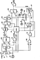
- an 8 bit serial PCM signal is connected from an input 10 to a serial-to-parallel converter 11 driven by a 64 KHz clock 12 (assuming single channel operation).
- the PCM signal is modulated by FSK data having standard frequencies of 1270 Hz (mark) and 1070 Hz (space) at a 300 baud rate.
- the 8 bits are then coupled in parallel through a one frame delay register 13.
- the sign bit 7 from the converter 11 is connected together with the inverted and delayed sign bit from the register 13, to an AND gate 14 in order to detect a change in the sign bit indicating a positive-going zero crossing of the encoded FSK signal at its output. Both the zero crossing signal and the clock are connected to the input of a sequence timing control 15.
- the six most significant magnitude bits 6-1 from the converter 11 and the register 13 are connected to an interpolation read-only-memory (ROM) 20 which generates at its output a 4 bit digital signal based on the equivalent linear values of the magnitude of the sample suceeding the zero crossing divided by the sum of the succeeding sample and the one preceding it (i.e. the one immediately preceding the zero crossing). This indicates the relevent position of the zero crossing with respect to the succeeding sampling instant of the pulse code modulated signal. While sinusoidal interpolation might be used in specific applications, straight line or linear interpolation was found to give better results when the incoming signal was unknown. Both this signal and a 4 bit binary signal equivalent to the maximum count of 15 from the ROM 20, are connected to a multiplexer 21.
- the sequence timing control 15 connects the output from the ROM 20 through the multiplexer 21 to the B input of an arithmetic logic unit 22. Conversely, when no zero crossing is detected, the 4 digit binary signal equivalent to a maximum count of 15, is connected to the B input of the arithmetic logic unit 22.
- the complement of the digital signal on the B input of the arithmetic logic unit 22 is added to that which is present at its A input (i.e. the current sum in the accumulator 23).
- the accumulator 23 is then updated with this new sum which is transferred through an 8 bit . line under control of the control unit 15. After this sum is processed, the accumulator 23 is immediately initialized for the next calculation, with the same digital signal (i.e. not its complement) on the B input. Thereafter, when each PCM signal sample occurs with no detection of a change in the sign bit, the maximum count of 15 at the B input is added to the current number in the accumulator 23 which is present at the A input of the arithmetic logic unit 22.
- the accumulator 23 is then updated with this new total. This continues until the next change in the sign bit is detected whereupon the logic unit 22 adds the complement of the next following interpolated signal count from the output of the ROM 20, so that the difference between the maximum count of 15 and the next following interpolated signal count, is added to and then stored in the accumulator 23. Under control of the timing control 15, a comparator 25 then compares the 8 bit summed output of the accumulator 23 at its A input against an 8 bit binary number of 103 at its threshold input T. Then, the accumulator 23 is again initialized for the next calculation.
- the average of these two is then 103 which is the reference number utilized in the comparator 25.
- Additional signal level and carrier frequency checks are also made before acceptance of the demodulated data signal from the NAND gate 26.
- the signal level is checked by determining the presence of either of the two most significant magnitude bits 6 or 5 from the output of the converter 11 to indicate whether a signal reference level of -30 DBM has been reached.
- an output from OR gate 30 is connected through an OR gate 31 to set a D flip-flop 32.
- the flip-flop 32 in turn is held in a latched condition by a return signal from its Q output coupled through the OR gate 31 until reset by the sequence counting control 15 after detection of a zero crossing.
- the 8 bit output of the accumulator 23 is also connected to the A input of comparator 35.
- Low and high binary reference signals representing a count of 33 and 128 respectively, are also connected to the comparator 35 so that an output will be obtained only when the count from the accumulator is between these two numbers. With 120 KHz sampling, these counts of 33 and 128 represent a frequency range from 3610 to 945 Hz respectively.
- the two outputs from the flip-flop 32 and the comparator 35 produce an output from AND gate 36 which is connected to an accumulator 37 having minimum and maximum limits of 0 and 255.
- an output is obtained on the most significant bit stage which then opens the NAND gate 26 to couple the demodulated data to the output of the demodulator.
Priority Applications (1)
| Application Number | Priority Date | Filing Date | Title |
|---|---|---|---|
| AT81304076T ATE17293T1 (de) | 1980-09-25 | 1981-09-07 | Demodulator fuer frequenzumgetastete daten. |
Applications Claiming Priority (2)
| Application Number | Priority Date | Filing Date | Title |
|---|---|---|---|
| CA000361021A CA1137632A (fr) | 1980-09-25 | 1980-09-25 | Demodulateur de signaux modules par impulsions et codage initialement modules par deplacement de frequence |
| CA361021 | 1980-09-25 |
Publications (3)
| Publication Number | Publication Date |
|---|---|
| EP0049059A2 true EP0049059A2 (fr) | 1982-04-07 |
| EP0049059A3 EP0049059A3 (en) | 1982-12-01 |
| EP0049059B1 EP0049059B1 (fr) | 1986-01-02 |
Family
ID=4117988
Family Applications (1)
| Application Number | Title | Priority Date | Filing Date |
|---|---|---|---|
| EP81304076A Expired EP0049059B1 (fr) | 1980-09-25 | 1981-09-07 | Démodulateur d'impulsions codées pour données modulées par déplacement de fréquence |
Country Status (5)
| Country | Link |
|---|---|
| EP (1) | EP0049059B1 (fr) |
| JP (1) | JPS5787267A (fr) |
| AT (1) | ATE17293T1 (fr) |
| CA (1) | CA1137632A (fr) |
| DE (1) | DE3173373D1 (fr) |
Cited By (4)
| Publication number | Priority date | Publication date | Assignee | Title |
|---|---|---|---|---|
| EP0099142A2 (fr) * | 1982-06-23 | 1984-01-25 | Philips Patentverwaltung GmbH | Procédé et dispositif de démodulation d'un signal d'entrée modulé en fréquence |
| EP0170324A1 (fr) * | 1984-07-23 | 1986-02-05 | Koninklijke Philips Electronics N.V. | Dispositif de génération d'un signal porteur modulé en angle et à amplitude constante en réponse aux signaux de données |
| WO1993010611A1 (fr) * | 1991-11-14 | 1993-05-27 | Northern Telecom Limited | Demodulateur digital mdf (modulation par deplacement de frequence) |
| ES2089934A1 (es) * | 1992-10-15 | 1996-10-01 | Mateo Francisco Manas | Procedimiento para la transmision y/o almacenamiento de señales voz/datos/imagen. |
Citations (4)
| Publication number | Priority date | Publication date | Assignee | Title |
|---|---|---|---|---|
| GB1201216A (en) * | 1967-04-24 | 1970-08-05 | Gen Electric | Improvements in f.s.k. receiver |
| GB1465871A (en) * | 1974-01-16 | 1977-03-02 | Oki Electric Ind Co Ltd | Pcm encoding device and a method of encoding a pcm signal from a corresponding pam signal |
| CH601954A5 (fr) * | 1975-06-27 | 1978-07-14 | Siemens Ag Albis | |
| GB2000345A (en) * | 1977-06-10 | 1979-01-04 | Cit Alcatel | Device for detecting a frequency in a pcm coded signal |
-
1980
- 1980-09-25 CA CA000361021A patent/CA1137632A/fr not_active Expired
-
1981
- 1981-09-07 EP EP81304076A patent/EP0049059B1/fr not_active Expired
- 1981-09-07 DE DE8181304076T patent/DE3173373D1/de not_active Expired
- 1981-09-07 AT AT81304076T patent/ATE17293T1/de active
- 1981-09-24 JP JP56149686A patent/JPS5787267A/ja active Granted
Patent Citations (4)
| Publication number | Priority date | Publication date | Assignee | Title |
|---|---|---|---|---|
| GB1201216A (en) * | 1967-04-24 | 1970-08-05 | Gen Electric | Improvements in f.s.k. receiver |
| GB1465871A (en) * | 1974-01-16 | 1977-03-02 | Oki Electric Ind Co Ltd | Pcm encoding device and a method of encoding a pcm signal from a corresponding pam signal |
| CH601954A5 (fr) * | 1975-06-27 | 1978-07-14 | Siemens Ag Albis | |
| GB2000345A (en) * | 1977-06-10 | 1979-01-04 | Cit Alcatel | Device for detecting a frequency in a pcm coded signal |
Cited By (5)
| Publication number | Priority date | Publication date | Assignee | Title |
|---|---|---|---|---|
| EP0099142A2 (fr) * | 1982-06-23 | 1984-01-25 | Philips Patentverwaltung GmbH | Procédé et dispositif de démodulation d'un signal d'entrée modulé en fréquence |
| EP0099142A3 (en) * | 1982-06-23 | 1985-08-21 | Philips Patentverwaltung Gmbh | Method and device for the demodulation of a frequency-modulated input signal |
| EP0170324A1 (fr) * | 1984-07-23 | 1986-02-05 | Koninklijke Philips Electronics N.V. | Dispositif de génération d'un signal porteur modulé en angle et à amplitude constante en réponse aux signaux de données |
| WO1993010611A1 (fr) * | 1991-11-14 | 1993-05-27 | Northern Telecom Limited | Demodulateur digital mdf (modulation par deplacement de frequence) |
| ES2089934A1 (es) * | 1992-10-15 | 1996-10-01 | Mateo Francisco Manas | Procedimiento para la transmision y/o almacenamiento de señales voz/datos/imagen. |
Also Published As
| Publication number | Publication date |
|---|---|
| EP0049059B1 (fr) | 1986-01-02 |
| CA1137632A (fr) | 1982-12-14 |
| EP0049059A3 (en) | 1982-12-01 |
| JPS5787267A (en) | 1982-05-31 |
| DE3173373D1 (en) | 1986-02-13 |
| ATE17293T1 (de) | 1986-01-15 |
| JPH0136747B2 (fr) | 1989-08-02 |
Similar Documents
| Publication | Publication Date | Title |
|---|---|---|
| US4007330A (en) | Method and apparatus for demodulation of relative phase modulated binary data | |
| EP0453063A2 (fr) | Décodage de signaux biphasé en mesurant la longueur des impulsions | |
| CA1039420A (fr) | Detecteur de signaux vocaux codes | |
| WO1983001159A1 (fr) | Interpolateur a croisement zero permettant de reduire la distorsion isochrone dans un modem numerique a modulation par deplacement de frequence | |
| US4378526A (en) | Pulse code demodulator for frequency shift keyed data | |
| EP0049059A2 (fr) | Démodulateur d'impulsions codées pour données modulées par déplacement de fréquence | |
| GB1471419A (en) | Signal conversion system | |
| US3875333A (en) | Method of eliminating errors of discrimination due to intersymbol interference and a device for using the method | |
| US4458206A (en) | Circuit for synchronizing the demodulation of phase modulated transmission bursts | |
| US3746995A (en) | Digital demodulator for phase-modulated data transmission systems | |
| EP0371357B1 (fr) | Méthode de détermination du temps de réception d'un signal au moyen d'une technique de corrélation | |
| EP0118234B1 (fr) | Démodulateur cohérent à déplacement déphasé comportant un appareil d'échantillonnage et procédé correspondant | |
| US4644563A (en) | Data transmission method and system | |
| US5226062A (en) | Method and device for detecting multi-level digital signal data stream termination | |
| EP0643511A1 (fr) | Circuit de synchronisation pour un signal avec sousporteuses | |
| US6990157B2 (en) | All-digital FSK demodulation with selectable data rate and adjustable resolution | |
| KR100435560B1 (ko) | 디퍼런셜 코드를 마이컴에서 수신하는 방법 | |
| JP2627890B2 (ja) | デコード回路 | |
| SU1628217A2 (ru) | Устройство дл демодул ции цифровых сигналов с частотной модул цией | |
| SU834907A1 (ru) | Устройство дл анализа импульсныхпОСлЕдОВАТЕльНОСТЕй | |
| KR100526938B1 (ko) | 디퍼런셜코드를마이컴에서수신하는방법 | |
| KR100435559B1 (ko) | 디퍼런셜 코드를 마이컴에서 수신하는 방법 | |
| SU1307600A1 (ru) | Устройство дл приема сигналов данных | |
| JPS5765939A (en) | Digital information communication system | |
| KR20000003082A (ko) | 디퍼런셜 코드를 마이컴에서 수신하는 방법 |
Legal Events
| Date | Code | Title | Description |
|---|---|---|---|
| PUAI | Public reference made under article 153(3) epc to a published international application that has entered the european phase |
Free format text: ORIGINAL CODE: 0009012 |
|
| AK | Designated contracting states |
Designated state(s): AT DE FR GB |
|
| PUAL | Search report despatched |
Free format text: ORIGINAL CODE: 0009013 |
|
| AK | Designated contracting states |
Designated state(s): AT DE FR GB |
|
| 17P | Request for examination filed |
Effective date: 19830207 |
|
| GRAA | (expected) grant |
Free format text: ORIGINAL CODE: 0009210 |
|
| AK | Designated contracting states |
Designated state(s): AT DE FR GB |
|
| REF | Corresponds to: |
Ref document number: 17293 Country of ref document: AT Date of ref document: 19860115 Kind code of ref document: T |
|
| REF | Corresponds to: |
Ref document number: 3173373 Country of ref document: DE Date of ref document: 19860213 |
|
| ET | Fr: translation filed | ||
| PLBE | No opposition filed within time limit |
Free format text: ORIGINAL CODE: 0009261 |
|
| STAA | Information on the status of an ep patent application or granted ep patent |
Free format text: STATUS: NO OPPOSITION FILED WITHIN TIME LIMIT |
|
| 26N | No opposition filed | ||
| PGFP | Annual fee paid to national office [announced via postgrant information from national office to epo] |
Ref country code: AT Payment date: 19900913 Year of fee payment: 10 |
|
| PGFP | Annual fee paid to national office [announced via postgrant information from national office to epo] |
Ref country code: FR Payment date: 19900919 Year of fee payment: 10 |
|
| PGFP | Annual fee paid to national office [announced via postgrant information from national office to epo] |
Ref country code: DE Payment date: 19901031 Year of fee payment: 10 |
|
| PG25 | Lapsed in a contracting state [announced via postgrant information from national office to epo] |
Ref country code: AT Effective date: 19910907 |
|
| PG25 | Lapsed in a contracting state [announced via postgrant information from national office to epo] |
Ref country code: FR Effective date: 19920529 |
|
| PG25 | Lapsed in a contracting state [announced via postgrant information from national office to epo] |
Ref country code: DE Effective date: 19920602 |
|
| REG | Reference to a national code |
Ref country code: FR Ref legal event code: ST |
|
| PGFP | Annual fee paid to national office [announced via postgrant information from national office to epo] |
Ref country code: GB Payment date: 19960830 Year of fee payment: 16 |
|
| PG25 | Lapsed in a contracting state [announced via postgrant information from national office to epo] |
Ref country code: GB Free format text: LAPSE BECAUSE OF NON-PAYMENT OF DUE FEES Effective date: 19970907 |
|
| GBPC | Gb: european patent ceased through non-payment of renewal fee |
Effective date: 19970907 |