EP0047686B1 - Mélangeur hybride hyperfréquence - Google Patents
Mélangeur hybride hyperfréquence Download PDFInfo
- Publication number
- EP0047686B1 EP0047686B1 EP81401306A EP81401306A EP0047686B1 EP 0047686 B1 EP0047686 B1 EP 0047686B1 EP 81401306 A EP81401306 A EP 81401306A EP 81401306 A EP81401306 A EP 81401306A EP 0047686 B1 EP0047686 B1 EP 0047686B1
- Authority
- EP
- European Patent Office
- Prior art keywords
- mixer
- waveguide
- ring
- frequency
- transformers
- Prior art date
- Legal status (The legal status is an assumption and is not a legal conclusion. Google has not performed a legal analysis and makes no representation as to the accuracy of the status listed.)
- Expired
Links
Images

Classifications
-
- H—ELECTRICITY
- H01—ELECTRIC ELEMENTS
- H01P—WAVEGUIDES; RESONATORS, LINES, OR OTHER DEVICES OF THE WAVEGUIDE TYPE
- H01P5/00—Coupling devices of the waveguide type
- H01P5/12—Coupling devices having more than two ports
- H01P5/16—Conjugate devices, i.e. devices having at least one port decoupled from one other port
- H01P5/19—Conjugate devices, i.e. devices having at least one port decoupled from one other port of the junction type
- H01P5/22—Hybrid ring junctions
- H01P5/222—180° rat race hybrid rings
-
- H—ELECTRICITY
- H03—ELECTRONIC CIRCUITRY
- H03D—DEMODULATION OR TRANSFERENCE OF MODULATION FROM ONE CARRIER TO ANOTHER
- H03D9/00—Demodulation or transference of modulation of modulated electromagnetic waves
- H03D9/06—Transference of modulation using distributed inductance and capacitance
- H03D9/0608—Transference of modulation using distributed inductance and capacitance by means of diodes
- H03D9/0633—Transference of modulation using distributed inductance and capacitance by means of diodes mounted on a stripline circuit
-
- H—ELECTRICITY
- H03—ELECTRONIC CIRCUITRY
- H03D—DEMODULATION OR TRANSFERENCE OF MODULATION FROM ONE CARRIER TO ANOTHER
- H03D2200/00—Indexing scheme relating to details of demodulation or transference of modulation from one carrier to another covered by H03D
- H03D2200/0001—Circuit elements of demodulators
- H03D2200/0003—Rat race couplers
-
- H—ELECTRICITY
- H03—ELECTRONIC CIRCUITRY
- H03D—DEMODULATION OR TRANSFERENCE OF MODULATION FROM ONE CARRIER TO ANOTHER
- H03D2200/00—Indexing scheme relating to details of demodulation or transference of modulation from one carrier to another covered by H03D
- H03D2200/0001—Circuit elements of demodulators
- H03D2200/0023—Balun circuits
-
- H—ELECTRICITY
- H03—ELECTRONIC CIRCUITRY
- H03D—DEMODULATION OR TRANSFERENCE OF MODULATION FROM ONE CARRIER TO ANOTHER
- H03D7/00—Transference of modulation from one carrier to another, e.g. frequency-changing
- H03D7/14—Balanced arrangements
- H03D7/1408—Balanced arrangements with diodes
Definitions
- the present invention relates to hybrid microwave mixers, which allow from two radio signals to obtain a third radio signal whose frequency is equal to the difference of those of the first two signals.
- Such mixers are particularly useful for coherent Doppler radars in which all the signals are obtained from a local quartz oscillator whose frequency and phase are very stable.
- a double frequency change is used in the reception chain.
- the first frequency change is carried out using a mixer receiving on the one hand the reception signal whose frequency is between 9300 and 9900 MHz, and on the other hand a signal coming from the chain of emission and whose frequency is between 7440 and 8040 MHz.
- the choice in these ranges is made on transmission and the frequency difference between these two signals is constant and equal to 1860 MHz.
- This frequency is that of the signal resulting from this mixing and obtained at the output of the mixer. It is relatively high and therefore requires special precautions in the production of the mixer to avoid losses and mismatches which could attenuate the intermediate frequency signal thus obtained too much.
- the invention provides a hybrid microwave mixer, of the type comprising a type 2 mixer ring, a first waveguide connected at a first point on the outside of this ring to bring it a first signal having a first frequency, a second waveguide connected on the outside of the ring at a second point to --- from the first point to bring to the ring a second signal having a second frequency, these first and second frequencies determining the parameter ⁇ , a first and a second diode connected on one side to the ring respectively on either side of the first point at 4 and on the other side at a third waveguide which makes it possible to deliver a third signal whose frequency is the difference of the first and second frequencies, characterized in that the ring, the first and the second waveguides, are etched on a first metallic layer eu based on a first dielectric layer, in that the third waveguide is etched on a second metal layer resting on a second dielectric layer superimposed on the first di
- a common technology for producing microwave circuits consists in using a plate formed of a dielectric layer sandwiched between a first solid metal layer forming a ground plane, and a second metal layer on which one has been etched, by chemical attack for example, connections forming lines, or microwave guides.
- the characteristic impedance of these lines depends on the width of the connections and the permittivity of the dielectric.
- the wavelength in the guides depends on this same permittivity. It is thus possible to obtain reasonable dimensions even at very high frequencies, and the desirable impedance for the connections of the devices and their elements between them, by playing on this width and this permittivity.
- This technology is also known by the Anglo-Saxon term of "micro-strip".
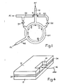
- a mixer such as that shown in FIG. 1. It comprises an AM ring whose circumference measures three half-wavelengths, that is to say , in the circuit at an average frequency between that of the signal on reception and that of the local oscillator.
- the RF reception signal is applied to a first waveguide G1 connected to the outside of the ring AM at a first point.
- the OL signal from the local oscillator is applied to a second waveguide G2 connected to the outside of the ring at a distance equal to the first point.
- a first mixing diode D 1 is connected by its cathode to a short guide fragment connected to the outside of the ring at a midpoint relative to the two guides G1 and G2 and to these.
- a second mixing diode D2 is connected by its anode to another short guide fragment connected to the outside of the ring at a point located at from G1 and to of G2.
- the anode of D and the cathode of D2 are connected by two other short fragments of guides to a third guide G3 at the end of which appears the IF signal at intermediate frequency resulting from the mixing between the signals RL and OL.
- the circuits located on either side of the diodes D 1 and D2 are separated by making them separately on the layers reserved for the guides of two metal-dielectric sandwiches. These sandwiches are then brought together by superimposing them to bring the layers forming ground planes into contact, and with an arrangement such that the connection points of the signal output guide at intermediate frequency to the mixing diodes substantially coincide with the connection points of these diodes with the ring.
- the electrical continuity of the ground planes and the immobilization of the sandwiches with respect to each other are obtained for example by welding these planes one on the other.
- the sandwiches are drilled at the location of the connections, and microwaves are inserted into these holes. The width of such a box is such that it corresponds substantially to the thickness of the two superimposed sandwiches and therefore the outlet connections of these boxes are at the points to which they must be connected on the engraved faces of the sandwiches.
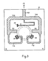
- FIGS. 2 and 3 The two engraved faces of the two sandwiches used in a particular embodiment of such a mixer have been shown in FIGS. 2 and 3, in a direction such that the letters D and G are superimposed when these sandwiches are placed back to back.
- This particular embodiment corresponds to a mixer that can operate in the frequency range mentioned above, and the drawing is substantially on a scale of 4 for a dielectric material whose thickness is 0.8 mm and the relative permittivity of 2.2 .
- the face shown in FIG. 2 comprises on the surface of a dielectric plate 21 of substantially square shape a ring AM of dimensions , a guide G1 connected to this ring, and a guide G2 connected to the ring at a distance of of the connection point of G 1.
- the guides G 1 and G2 make it possible to receive respectively the signals of reception RF and of the local oscillator OL.
- Two substantially rectangular holes 22 and 23 have been made in the thickness of the dielectric and of the ground plane situated below the latter in the figure. So they go right through the sandwich. They are located so as to tangent the ring AM at two points located on either side of the connection points of the guide G1 at a distance of .
- Two holes 32 and 33 which are superimposed on the holes 22 and 23 are also drilled in the dielectric plate and in the ground plane situated under it.
- the AM ring is shown by transparency to clearly show its location in relation to holes 32 and 33.
- the microwave diodes have the shape of two small parallelepipedic boxes provided on two opposite faces with the tabs forming the output connections.
- the value of the distance between these opposite faces is substantially the same as that of the thickness of the two sandwiches when they are welded to each other by their ground planes.
- the dimensions of the holes 22, 23, 32, 33 are determined to place these soft friction housings. It is then enough to put the diodes in the holes in the right direction, and then to fold over the connections engraved on the sandwiches the tabs which overflow on each side. We finish by welding on these connections the folded tabs.
- the impedance of these diodes at the working frequencies used is approximately 250 n.
- the impedance of each one brought back to their junction at G3 must be 100 u.
- To obtain a transformer of the quarter-wave type giving this result, it would be necessary that the impedance of this one is approximately 158 u.
- the width of a guide having this impedance is small and leads to great difficulties in production.
- the first two transformers for each diode are respectively T13 and T12, with an impedance substantially equal to 72 ⁇ , and the two second transformers, respectively T23 and T22, with an impedance substantially equal to 44 ⁇ .
- These transformers are folded to occupy less than place and surround the location of the AM ring following the sides of the plate 31 to join the end of the guide G3 by forming a T at this location.
- the longitudinal dimension transformers is of course calculated from the frequency of the signal FI emitted at the output of G3 since it is the useful signal extracted from the diodes. We take the mediating value of the range occupied by FI.
- two traps P3 and P2 which eliminate these unwanted signals are placed perpendicularly to T23 and T32, not far from their junctions with T13 and T12. They are tuned to the most probable spurious signal, that is to say to the OL signal whose level is much higher than the RF signal. In addition RF will still be attenuated since its frequency is not too far from that of OL, and due to its low level, it will also be eliminated.
- a shock inductance L is used, produced in the form of a length guide fragment. (at the frequency of IF), one end of which is connected to the junction point of G3, T23 and T22, and the other to ground via a hole 35 drilled in the plate 31 and which makes it possible to connect it , for example by a drop of solder, to the ground plane located between the plates 21 and 31.
- the impedance being zero (at the frequency of FI) on this ground plane, it is infinite at the other end, which prevents FI from passing but lets the DC bias current pass.
- This inductance L is located, as well as the traps P2 and P3 in the space left free in the middle of the wafer by the tuning transformers of the diodes. It is folded down to take place in this space.
- FIG. 4 therefore shows a means of easily obtaining such contact.
- the mixer shown in this figure has been limited to the two sandwiches placed side by side without showing the circuits illustrated elsewhere in Figures 2 and 3. There are therefore two dielectric plates 21 and 31 placed one on top of the other with them the two metal layers 24 and 34 welded together.
- a notch 41 has been cut along the edge which is, in the example illustrated, of rectangular shape. This allows a sufficiently large part of the surface of the layer 24 to be cleared to weld a ground wire 42.
- the invention also extends to the case where a sandwich formed of two dielectric layers enclosing a single metal layer forming a ground plane and covered with two external metal layers making it possible to etch the waveguides is used as the starting material. In this case the layers 24 and 34 are combined.
Applications Claiming Priority (2)
| Application Number | Priority Date | Filing Date | Title |
|---|---|---|---|
| FR8019414 | 1980-09-09 | ||
| FR8019414A FR2490023A1 (fr) | 1980-09-09 | 1980-09-09 | Melangeur hybride hyperfrequence |
Publications (2)
| Publication Number | Publication Date |
|---|---|
| EP0047686A1 EP0047686A1 (fr) | 1982-03-17 |
| EP0047686B1 true EP0047686B1 (fr) | 1984-11-14 |
Family
ID=9245767
Family Applications (1)
| Application Number | Title | Priority Date | Filing Date |
|---|---|---|---|
| EP81401306A Expired EP0047686B1 (fr) | 1980-09-09 | 1981-08-14 | Mélangeur hybride hyperfréquence |
Country Status (5)
| Country | Link |
|---|---|
| US (1) | US4377005A (ja) |
| EP (1) | EP0047686B1 (ja) |
| JP (1) | JPS5779716A (ja) |
| DE (1) | DE3167204D1 (ja) |
| FR (1) | FR2490023A1 (ja) |
Families Citing this family (16)
| Publication number | Priority date | Publication date | Assignee | Title |
|---|---|---|---|---|
| US4654887A (en) * | 1985-11-04 | 1987-03-31 | Raytheon Company | Radio frequency mixer |
| US4811426A (en) * | 1987-05-07 | 1989-03-07 | Martin Marietta Corporation | Suspended stripline rat race mixer with simplified I. F. extraction |
| US5062149A (en) * | 1987-10-23 | 1991-10-29 | General Dynamics Corporation | Millimeter wave device and method of making |
| FR2628893B1 (fr) * | 1988-03-18 | 1990-03-23 | Thomson Csf | Interrupteur hyperfrequence |
| US4949398A (en) * | 1988-06-09 | 1990-08-14 | The Aerospace Corporation | GaAs MESFET balanced resistive mixer |
| US5303419A (en) * | 1992-05-29 | 1994-04-12 | Her Majesty The Queen In Right Of Canada As Represented By The Minister Of Communications | Aperture-coupled line Magic-Tee and mixer formed therefrom |
| GB9410985D0 (en) * | 1994-06-01 | 1994-07-20 | Plessey Semiconductors Ltd | Radar transmitter/receivers |
| GB2290000B (en) * | 1994-06-01 | 1998-02-25 | Plessey Semiconductors Ltd | Radar transmitter/receivers |
| US5978666A (en) * | 1994-09-26 | 1999-11-02 | Endgate Corporation | Slotline-mounted flip chip structures |
| US5983089A (en) * | 1994-09-26 | 1999-11-09 | Endgate Corporation | Slotline-mounted flip chip |
| US6094114A (en) * | 1994-09-26 | 2000-07-25 | Endgate Corporation | Slotline-to-slotline mounted flip chip |
| US6265937B1 (en) | 1994-09-26 | 2001-07-24 | Endgate Corporation | Push-pull amplifier with dual coplanar transmission line |
| GB2302773B (en) * | 1995-06-29 | 1999-12-22 | Pyronix Ltd | Improvements in or relating to motion detection units |
| US5903827A (en) * | 1995-07-07 | 1999-05-11 | Fujitsu Compound Semiconductor, Inc. | Single balanced frequency downconverter for direct broadcast satellite transmissions and hybrid ring signal combiner |
| KR100223375B1 (ko) * | 1997-06-11 | 1999-10-15 | 윤종용 | 마이크로웨이브 시스템에 사용하기 위한 주파수변환기 |
| GB2474710A (en) * | 2009-10-26 | 2011-04-27 | Applied Technology | A Radio Frequency Divider / Combiner with a low loss transmission mode by connection of short circuits to ports |
Family Cites Families (9)
| Publication number | Priority date | Publication date | Assignee | Title |
|---|---|---|---|---|
| US3512091A (en) * | 1965-10-22 | 1970-05-12 | Motorola Inc | Compact strip-line type mixer using hybrid ring |
| US3818385A (en) * | 1972-09-21 | 1974-06-18 | Aertech | Hybrid junction and mixer or modulator |
| GB1474291A (en) * | 1973-08-23 | 1977-05-18 | Siemens Ag | Frequency-changer structures |
| US3950703A (en) * | 1975-02-03 | 1976-04-13 | The United States Of America As Represented By The Secretary Of The Navy | Microcircuit reverse-phased hybrid ring mixer |
| DE2525468C3 (de) * | 1975-06-07 | 1980-03-13 | Licentia Patent-Verwaltungs-Gmbh, 6000 Frankfurt | Breitbandiger Mischer für sehr hohe Frequenzen in Streifenleitungstechnik |
| FR2395618A1 (fr) * | 1977-06-24 | 1979-01-19 | Lignes Telegraph Telephon | Procede de realisation de circuits micro-ondes integres complexes |
| US4186352A (en) * | 1978-03-23 | 1980-01-29 | Rockwell International Corporation | Signal converter apparatus |
| DE2819838C3 (de) * | 1978-05-05 | 1981-03-26 | Siemens AG, 1000 Berlin und 8000 München | Breitbandiger Ringmodulator für sehr kurze elektromagnetische Wellen |
| JPS5563106A (en) * | 1978-11-06 | 1980-05-13 | Hitachi Ltd | Mixer circuit |
-
1980
- 1980-09-09 FR FR8019414A patent/FR2490023A1/fr active Granted
-
1981
- 1981-08-14 DE DE8181401306T patent/DE3167204D1/de not_active Expired
- 1981-08-14 EP EP81401306A patent/EP0047686B1/fr not_active Expired
- 1981-08-27 US US06/297,043 patent/US4377005A/en not_active Expired - Fee Related
- 1981-09-08 JP JP56140407A patent/JPS5779716A/ja active Pending
Also Published As
| Publication number | Publication date |
|---|---|
| JPS5779716A (en) | 1982-05-19 |
| FR2490023B1 (ja) | 1984-05-04 |
| DE3167204D1 (en) | 1984-12-20 |
| US4377005A (en) | 1983-03-15 |
| EP0047686A1 (fr) | 1982-03-17 |
| FR2490023A1 (fr) | 1982-03-12 |
Similar Documents
| Publication | Publication Date | Title |
|---|---|---|
| EP0047686B1 (fr) | Mélangeur hybride hyperfréquence | |
| EP0013222B1 (fr) | Déphaseur hyperfréquence à diodes et antenne à balayage électronique comportant un tel déphaseur | |
| EP1172885B1 (fr) | Antenne à couche conductrice et dispositif de transmission bi-bande incluant cette antenne. | |
| EP0954055B1 (fr) | Antenne bifréquence pour la radiocommunication réalisée selon la technique des microrubans | |
| EP0627765B1 (fr) | Dispositif semiconducteur incluant un élément semiconducteur du type "FLIP-CHIP" | |
| FR2772517A1 (fr) | Antenne multifrequence realisee selon la technique des microrubans et dispositif incluant cette antenne | |
| EP1145378A1 (fr) | Dispositif de transmission bi-bande et antenne pour ce dispositif | |
| EP0210903A1 (fr) | Dispositif de couplage entre un guide d'onde métallique, un guide d'onde diélectrique et un composant semiconducteur, et mélangeur utilisant ce dispositif de couplage | |
| EP1073143A1 (fr) | Antenne imprimée bi-polarisation et réseau d'antennes correspondant | |
| FR2819109A1 (fr) | Antenne multi-bandes pour appareils mobiles | |
| FR2690020A1 (fr) | Circuit mélangeur. | |
| EP0015838B1 (fr) | Mélangeur hyperfréquence à large bande | |
| EP0005403A1 (fr) | Oscillateur monomode en hyperfréquences, accordable par variation d'un champ magnétique | |
| EP0335788B1 (fr) | Circuit déphaseur hyperfréquence | |
| EP2351143B1 (fr) | Coupleur radiofrequence compact | |
| EP0044774B1 (fr) | Mélangeur hybride à élévation de fréquence | |
| FR2780546A1 (fr) | Circuit integre monolithique comprenant une inductance plane ou un transformateur plan, et procede de fabrication d'un tel circuit | |
| EP0326498B1 (fr) | Circuit résonnant et filtre utilisant ce circuit | |
| EP0983616B1 (fr) | Procede et dispositif pour connecter deux elements millimetriques | |
| EP0102888B1 (fr) | Mélangeur d'ondes électromagnétiques hyperfréquences à récupération de la fréquence somme | |
| EP0274073B1 (fr) | Dispositif mélangeur doublement équilibré | |
| FR2508256A1 (fr) | Convertisseur de frequence equilibre double simplifie | |
| FR2494917A1 (fr) | Coupleur hybride hyperfrequence a large bande et melangeur equilibre le comportant | |
| EP2744311A1 (fr) | Procede de realisation de motifs resonnants adaptes a la realisation de fonctions passives RF | |
| FR2496997A1 (fr) | Dispositif de reglage de l'accord d'une ligne de transmission resonnante, ligne de transmission et filtre de bande hyperfrequence munis de tels dispositifs. |
Legal Events
| Date | Code | Title | Description |
|---|---|---|---|
| PUAI | Public reference made under article 153(3) epc to a published international application that has entered the european phase |
Free format text: ORIGINAL CODE: 0009012 |
|
| AK | Designated contracting states |
Designated state(s): BE DE GB IT SE |
|
| 17P | Request for examination filed |
Effective date: 19820325 |
|
| ITF | It: translation for a ep patent filed |
Owner name: JACOBACCI & PERANI S.P.A. |
|
| GRAA | (expected) grant |
Free format text: ORIGINAL CODE: 0009210 |
|
| AK | Designated contracting states |
Designated state(s): BE DE GB IT SE |
|
| REF | Corresponds to: |
Ref document number: 3167204 Country of ref document: DE Date of ref document: 19841220 |
|
| PLBE | No opposition filed within time limit |
Free format text: ORIGINAL CODE: 0009261 |
|
| STAA | Information on the status of an ep patent application or granted ep patent |
Free format text: STATUS: NO OPPOSITION FILED WITHIN TIME LIMIT |
|
| 26N | No opposition filed | ||
| PG25 | Lapsed in a contracting state [announced via postgrant information from national office to epo] |
Ref country code: SE Effective date: 19870815 |
|
| PG25 | Lapsed in a contracting state [announced via postgrant information from national office to epo] |
Ref country code: BE Effective date: 19880831 |
|
| BERE | Be: lapsed |
Owner name: LMT RADIO PROFESSIONNELLE Effective date: 19880831 |
|
| PG25 | Lapsed in a contracting state [announced via postgrant information from national office to epo] |
Ref country code: GB Effective date: 19890814 |
|
| GBPC | Gb: european patent ceased through non-payment of renewal fee | ||
| PG25 | Lapsed in a contracting state [announced via postgrant information from national office to epo] |
Ref country code: DE Effective date: 19900501 |
|
| EUG | Se: european patent has lapsed |
Ref document number: 81401306.6 Effective date: 19880711 |