EP0047196B1 - Structure optique intégrée à couplage directionnel conforme et système comprenant une telle structure - Google Patents
Structure optique intégrée à couplage directionnel conforme et système comprenant une telle structure Download PDFInfo
- Publication number
- EP0047196B1 EP0047196B1 EP81401257A EP81401257A EP0047196B1 EP 0047196 B1 EP0047196 B1 EP 0047196B1 EP 81401257 A EP81401257 A EP 81401257A EP 81401257 A EP81401257 A EP 81401257A EP 0047196 B1 EP0047196 B1 EP 0047196B1
- Authority
- EP
- European Patent Office
- Prior art keywords
- wave
- structure according
- transducer
- guides
- substrate
- Prior art date
- Legal status (The legal status is an assumption and is not a legal conclusion. Google has not performed a legal analysis and makes no representation as to the accuracy of the status listed.)
- Expired
Links
- 230000008878 coupling Effects 0.000 title claims description 32
- 238000010168 coupling process Methods 0.000 title claims description 32
- 238000005859 coupling reaction Methods 0.000 title claims description 32
- 230000003287 optical effect Effects 0.000 title claims description 18
- 239000000758 substrate Substances 0.000 claims description 16
- 230000005855 radiation Effects 0.000 claims description 10
- RTAQQCXQSZGOHL-UHFFFAOYSA-N Titanium Chemical compound [Ti] RTAQQCXQSZGOHL-UHFFFAOYSA-N 0.000 claims description 7
- 229910052719 titanium Inorganic materials 0.000 claims description 7
- 239000010936 titanium Substances 0.000 claims description 7
- 239000000463 material Substances 0.000 claims description 6
- 238000009792 diffusion process Methods 0.000 claims description 5
- GQYHUHYESMUTHG-UHFFFAOYSA-N lithium niobate Chemical compound [Li+].[O-][Nb](=O)=O GQYHUHYESMUTHG-UHFFFAOYSA-N 0.000 claims description 5
- 230000000750 progressive effect Effects 0.000 claims description 5
- 230000001360 synchronised effect Effects 0.000 claims description 4
- 230000005540 biological transmission Effects 0.000 claims description 2
- 210000001520 comb Anatomy 0.000 claims description 2
- 238000010586 diagram Methods 0.000 description 6
- 230000000694 effects Effects 0.000 description 4
- 238000000034 method Methods 0.000 description 4
- 230000005693 optoelectronics Effects 0.000 description 4
- 238000000206 photolithography Methods 0.000 description 4
- 230000005684 electric field Effects 0.000 description 3
- 230000006978 adaptation Effects 0.000 description 2
- 238000009826 distribution Methods 0.000 description 2
- 230000004907 flux Effects 0.000 description 2
- 238000004519 manufacturing process Methods 0.000 description 2
- 230000000644 propagated effect Effects 0.000 description 2
- 230000002745 absorbent Effects 0.000 description 1
- 239000002250 absorbent Substances 0.000 description 1
- 238000010521 absorption reaction Methods 0.000 description 1
- 230000008859 change Effects 0.000 description 1
- 230000000295 complement effect Effects 0.000 description 1
- 238000000151 deposition Methods 0.000 description 1
- 230000004069 differentiation Effects 0.000 description 1
- 230000005284 excitation Effects 0.000 description 1
- 230000006872 improvement Effects 0.000 description 1
- 238000002347 injection Methods 0.000 description 1
- 239000007924 injection Substances 0.000 description 1
- 230000003993 interaction Effects 0.000 description 1
- 238000010849 ion bombardment Methods 0.000 description 1
- 239000000203 mixture Substances 0.000 description 1
- 230000001151 other effect Effects 0.000 description 1
- 230000000737 periodic effect Effects 0.000 description 1
- 230000010287 polarization Effects 0.000 description 1
- 230000008569 process Effects 0.000 description 1
- 230000009467 reduction Effects 0.000 description 1
- 238000007493 shaping process Methods 0.000 description 1
- 239000000243 solution Substances 0.000 description 1
- 238000010897 surface acoustic wave method Methods 0.000 description 1
- 238000013519 translation Methods 0.000 description 1
- 230000014616 translation Effects 0.000 description 1
- 230000001960 triggered effect Effects 0.000 description 1
Images



Classifications
-
- G—PHYSICS
- G02—OPTICS
- G02F—OPTICAL DEVICES OR ARRANGEMENTS FOR THE CONTROL OF LIGHT BY MODIFICATION OF THE OPTICAL PROPERTIES OF THE MEDIA OF THE ELEMENTS INVOLVED THEREIN; NON-LINEAR OPTICS; FREQUENCY-CHANGING OF LIGHT; OPTICAL LOGIC ELEMENTS; OPTICAL ANALOGUE/DIGITAL CONVERTERS
- G02F1/00—Devices or arrangements for the control of the intensity, colour, phase, polarisation or direction of light arriving from an independent light source, e.g. switching, gating or modulating; Non-linear optics
- G02F1/29—Devices or arrangements for the control of the intensity, colour, phase, polarisation or direction of light arriving from an independent light source, e.g. switching, gating or modulating; Non-linear optics for the control of the position or the direction of light beams, i.e. deflection
- G02F1/33—Acousto-optical deflection devices
- G02F1/335—Acousto-optical deflection devices having an optical waveguide structure
Definitions
- the present invention relates to integrated optical structures implementing the guided propagation of optical radiation and more particularly to directional couplers.
- Evanescent waves create a coupling between the waveguides and it is sufficient that the guided waves have propagation speeds close enough to each other for an energy transfer to take place.
- With lossless waveguides a total transfer can be carried out which consists in collecting at the output of the second waveguide all the photons injected at the input of the first guide. Based on the electro-optical effect of the material used to make the integrated optical structure of a directional coupler, it is possible to electrically control the transfer of energy.
- This electrical control can take two aspects depending on whether the electric field is of electrostatic origin or produced by an electromagnetic wave capable of accompanying photons in their guided progression.
- the electric field When the electric field is stationary, the result of the transfer does not depend on the distribution of the photons so that the injected energy is switched or switched according to the electric control voltages applied to the electrodes of the structure.
- the command depends on an electromagnetic wave which accompanies the photons in their guided progression, each photon undergoes a different fate from its neighbors because the directional coupling which concerns it remains in conformity with an element of the invariant composition conveyed by the wave electromagnetic.
- the invention proposes to obtain the desired confinement by acting on the sections of waveguides reserved for the directional coupling of elastic waves capable of causing progressive index disturbance with the desired speed.
- the subject of the invention is an integrated optical structure with conformal directional coupling comprising a substrate on the surface of which are arranged two optical waveguides performing an energy exchange according to a predetermined coupling distance, this exchange being governed by conforming means. ensuring along this surface the synchronous propagation of an index disturbance accompanying the guided photons, this disturbance being induced by a progressive wave, characterized in that said shaping means comprise an electromechanical transducer for transmitting said wave, said progressive wave being an elastic surface wave, the obliquity of the wave fronts reaching said guides being such that it performs said synchronous propagation.
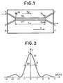
- FIG. 1 we see the structure of a directional coupler as we can achieve in integrated optics.
- This coupler comprises a substrate 7, for example made of lithium niobate, on the surface 8 of which two diffused regions 10 and 11 have been formed intended to guide optical radiation exchanged between channels 1-3 and 2-4.
- the variation in index necessary for guiding the light can be obtained by depositing a layer of titanium on the surface 8.
- the layer of titanium is removed except in line with the waveguides 10 and 11 and we proceed to the titanium diffusion operation deposited in the lithium niobate. After removal of the remaining titanium, two diffused bands are obtained surrounded by mediums of lower index. By giving these scattered bands an adequate width and depth of diffusion, two integrated single-mode waveguides are obtained.
- the waveguides 10 and 11 are brought closer to each other in a section of length L o which corresponds to the desired coupling distance.
- a wave 12 of determined wavelength is injected into channel 1, the latter propagates with the group velocity V g in the waveguide 10.
- the wave 12 can propagate to exchange part more or less of its energy with the structure of the waveguide 11.
- the energy exchange is done by evanescent waves in the section of approximation of the waveguides 10 and 11 where these are parallel to the axis x.
- the theoretical study of directional coupling uses the notion of a coupling coefficient c which is determined from the refractive indices, the width, the depth and the spacing of the waveguides 10 and 11 in the exchange section. This theory shows that the total transfer of energy takes place if the waveguides are lossless and if the propagation velocities have equal values. There is therefore a minimum coupling distance L o which, in the case of equality of group speeds, ensures a total transfer of energy between channels 1 and 4. Odd multiples of this distance give the same result.
- the ratio 1 of the energy coupled in channel 4 to the energy injected in channel 1 is equal to unity.
- the theory shows that the energy transfer ratio I is a function of the ratio ⁇ ⁇ / 2c.
- the ratio I can be in the form: Knowing that the total transfer takes place when: where k 'is a positive integer, it comes:
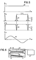
- FIG. 2 shows that the energy transfer can be modulated to obtain a distribution effect and, ultimately, a switching effect between channels 3 and 4.
- This modulation can be conceived statically or kinetically. It relates to the variation of index An which can be induced by an electro-optical effect and / or by any other effect such as the photoelastic effect.
- the variation of index An is in the form of a disturbance which accompanies the progression of the guided photons.
- This disturbance which propagates with the group speed V g presents around a zero value variations of index An sufficient to cancel the transfer ratio I.
- the photon sitting at the location of this zero value undergoes a transfer total, while its neighbors which throughout the coupling distance L o see a non-zero An, undergo a reduced transfer fixed by the diagram of FIG. 2.
- This kinetic conception of the modulation of the energy transfer in a coupler directional was proposed within the framework of structures using an electro-optical material.
- the index disturbance is induced by an electromagnetic line which straddles the directional coupler.
- the TEM mode propagated by the electromagnetic line must have a phase speed which coincides throughout the coupling section with the group speed V g . This condition is difficult to satisfy in practice, because the reduction in speed necessary to obtain the phase adaptation leads to serious manufacturing difficulties in the electromagnetic line.
- FIG. 3 represents an integrated optical structure according to the invention.
- the coupling section of length L o is aligned with the axis ox of a Cartesian reference system oxyz.
- the plane of the surface 8 is the oxy plane in which elastic surface waves are emitted, the wave fronts of which have as normal the direction U forming the angle 0 with the direction parallel to the axis oy.
- the emission of the elastic surface waves is ensured by an electromechanical transducer excited by an electric generator 9.
- This transducer comprises for example two electrodes 5 and 6 in the form of interdigitated combs.
- the configuration of the waveguides 10 and 11 as well as that of the electrodes 5 and 6 can be the subject of an extremely precise delimitation by photolithography. Elastic wave fronts can therefore meet the waveguides with a very low obliquity which retains its value over a long coupling length L o .
- the spacing of the waveguides 10 and 11 has been greatly exaggerated, as well as the inclination 0 of the teeth of the transducer 5, 6.
- FIG. 3 The operating mode of the structure of FIG. 3 can be better understood by means of FIGS. 4 and 5.
- FIG. 4 represents at a given instant the configuration of the mechanical stresses imposed by the surface elastic wave in the plane of the surface 8.
- the surface elastic wave may for example be a Rayleigh wave, but it can also be an interface wave.
- the axes X 1 and X 2 of the two guides 10 and 11 having a spacing a and their width b is less than a.
- the elastic surface wave is represented by wave fronts 19, 20, 21, 22, 23, 24 and 25 which meet the axes X 1 and X 2 with an inclination 0.
- the diagram A, u shows the variation of mechanical stress produced by the elastic wave. In the case of FIG. 4, this constraint evolves sinusoidally as shown by curve 18. This wave progresses with an acoustic speed V a measured perpendicular to the wave front.
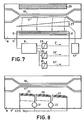
- FIG. 5 shows by curve 60 the incident power I 1 on channel 1 of the directional coupler.
- the constraint A imposed by the elastic surface wave is represented by the curve 63.
- These two curves are plotted with the same time scale t as reference.
- the powers 1 3 and 1 4 collected in the channels 3 and 4 are represented by the curves 62 and 61 which are complementary.
- Curves 61 and 62 have been plotted taking for the time scale, because we have taken into account of the transmission delay L o / V g over the coupling distance L o .
- the power in channel 4 is in the form of pulses having the profile of FIG. 2.
- the narrowness of these pulses is all the greater the greater the index gradient around the abscissae x o , X2 and x 4 .
- the period of the pulses is equal to half the period of the surface acoustic wave.
- the pulse train collected in channel 4 forms a periodic function regardless of the coupling length chosen. However, to carry out a total transfer, the length L o must be chosen appropriately.
- the excitation frequency of the electromechanical transducer f a is equal to 227 MHz.
- the interval between two coupled pulses in channel 4 is approximately 2.2 ns.
- ⁇ is the wavelength of optical radiation in a vacuum. In the case of monochromatic radiation, this duration has a defined value.
- the directional coupler of FIG. 3 makes it possible to envisage an electrical adjustment of the total transfer length.
- electrodes can be added as shown in FIG. 6.
- the guide 11 is covered over the entire coupling length by a first electrode 39, while the guide 10 is covered half by half by two electrodes 38 and 40.
- a generator 41 supplies the electrodes 38 and 40 with an adjustable bias voltage. By electro-optical effect, this voltage influences the phase constants so as to achieve a total transfer.
- FIG. 7 shows a transducer 5-6, the comb teeth of which are oriented parallel to the straight sections of the waveguides 10 and 11.
- Deviating means of elastic surface waves 27 are interposed between the transducer 5-6 and the directional coupling section 10 ⁇ 11.
- a deflecting means it is possible to use a prismatic zone dug in a bowl to carry out a geodesic type refraction.
- the absorption of the elastic surface waves can be ensured by a layer of absorbent material 26 placed downstream of the directional coupler.
- Another improvement illustrated in FIG. 7 consists in supplying the transducer 5-6 with several voltages of frequencies F, 3F, 5F. Adjustment circuits 28, 29 and 30 make it possible to adjust these voltages by amplitude and phase, to obtain at the meeting of the waveguides 10 and 11 a variation of index with steep front. This steep-front variation makes it possible to reduce the duration of the coupled pulses.
- FIG. 8 shows that the electromechanical transducer can be split into several sections 35, 36 and 37. By feeding these sections via phase-shifting circuits 31 and 32 connected to the supply terminals 33 and 34, it is possible to obtain slight deformations of the front d wave radiated so that its inclination 0 verifies the phase tuning condition.
- the phase shifting circuits 31 and 32 can advantageously be constituted by connections of adjustable length deposited on the substrate 8.
- a source of continuous monochromatic radiation 43 is coupled to channel 1 of the directional coupler 44.
- This coupler is placed under the control of an alternating generator 45 which supplies an electromechanical transducer.
- Channel 4 of coupler 44 delivers ultra short pulses at a frequency twice that of generator 45.
- the pulses delivered by directional coupler 44 are applied to channel 1 of a directional coupler 46 with a structure identical to that of coupler 44.
- Channels 3 and 4 of the coupler 46 are connected to radiation detectors 48 and 49 which supply the two inputs of a comparator circuit 50.
- the coupler 46 is placed under the control of an alternating generator 47 with adjustable tuning.
- the comparator circuit 50 controls the frequency tuning of the generator 47.
- the system of FIG. 9 makes it possible to set the frequency and in phase of the two clocks.
- the comparator circuit 50 prepares a tuning signal as a function of the transfer ratio measured by the two detectors 48 and 49.
- the timing of the clock 47 occurs when the channel 4 of the coupler 46 alone delivers the pulses injected in the channel 1.
- a new tuning setting is triggered by the comparator circuit 50 when the total transfer to channel 4 deteriorates.
- the invention is not limited to the case where a single directional coupler is placed on the path of the elastic waves.
- FIG. 10 we can see two structures of directional couplers 51 and 53 placed on either side of an electromechanical transducer 52.
- the teeth of the transducer 52 are inclined relative to the rectilinear sections of the two couplers 51 and 53.
- the waveguides are all parallel; the numbering of the channels indicates the direction in which the coupling takes place.
- Several directional couplers could be provided on each side of the electromechanical transducer 52.
- a directional coupler can be irradiated by the elastic waves coming from several transducers arranged on the substrate 7. By operating these transducers alternately and choosing the appropriate inclination of the wave fronts, it is possible to carry out a directional coupling in the two directions of circulation.
- the invention is not limited to transducers composed of interdigitated comb electrodes deposited on a piezoelectric substrate.
- the interaction described above does not imply that the substrate 7 is piezoelectric and that it is made of an electro-optical material.
- FIG. 11 a directional coupling device can be seen in which the elastic waves are emitted by an electromechanical transducer 55 emitting longitudinal or transverse waves.
- a coupling prism 54 adapts the speed of the waves emitted by the transducer 55 to that of the elastic waves propagated by the surface 8.
- the width of the pulses is given by the relation: equals unity when k equals a positive integer. On the other hand, this factor tends to infinity if k is equal to half of an odd number.
Landscapes
- Physics & Mathematics (AREA)
- Nonlinear Science (AREA)
- General Physics & Mathematics (AREA)
- Optics & Photonics (AREA)
- Optical Integrated Circuits (AREA)
Applications Claiming Priority (2)
| Application Number | Priority Date | Filing Date | Title |
|---|---|---|---|
| FR8018772A FR2490835A1 (fr) | 1980-08-29 | 1980-08-29 | Structure optique integree a couplage directionnel conforme |
| FR8018772 | 1980-08-29 |
Publications (2)
| Publication Number | Publication Date |
|---|---|
| EP0047196A1 EP0047196A1 (fr) | 1982-03-10 |
| EP0047196B1 true EP0047196B1 (fr) | 1983-09-28 |
Family
ID=9245504
Family Applications (1)
| Application Number | Title | Priority Date | Filing Date |
|---|---|---|---|
| EP81401257A Expired EP0047196B1 (fr) | 1980-08-29 | 1981-08-04 | Structure optique intégrée à couplage directionnel conforme et système comprenant une telle structure |
Country Status (5)
| Country | Link |
|---|---|
| US (1) | US4433895A (ref) |
| EP (1) | EP0047196B1 (ref) |
| JP (1) | JPS5774728A (ref) |
| DE (1) | DE3161033D1 (ref) |
| FR (1) | FR2490835A1 (ref) |
Families Citing this family (14)
| Publication number | Priority date | Publication date | Assignee | Title |
|---|---|---|---|---|
| DE3115562A1 (de) * | 1981-04-16 | 1982-11-11 | Siemens AG, 1000 Berlin und 8000 München | Optischer modulator, verfahren zu seinem betrieb und seine verwendung |
| US4674827A (en) * | 1982-05-20 | 1987-06-23 | Masayuki Izutsu | Slab-type optical device |
| JPS6085312A (ja) * | 1983-10-17 | 1985-05-14 | Hitachi Ltd | 固体化干渉計 |
| SE455892B (sv) * | 1984-02-17 | 1988-08-15 | Ericsson Telefon Ab L M | Optisk integrerad vagledarkomponent |
| US4791388A (en) * | 1987-04-27 | 1988-12-13 | Polaroid Corporation | Channel waveguide modulator |
| US4899042A (en) * | 1987-11-17 | 1990-02-06 | The Boeing Company | Integrated optic field sensor consisting of an interferometer formed in substrate |
| FR2635198B1 (fr) * | 1988-08-03 | 1992-09-04 | Commissariat Energie Atomique | Dispositif de commutation de faisceaux lumineux integre |
| US5313535A (en) * | 1992-02-27 | 1994-05-17 | Nynex Corporation | Optical path length modulator |
| US5446807A (en) * | 1994-06-23 | 1995-08-29 | Bell Communications Research, Inc. | Passband-flattened acousto-optic polarization converter |
| US5790720A (en) * | 1997-05-06 | 1998-08-04 | Lucent Technologies, Inc. | Acoustic-optic silica optical circuit switch |
| FR2784185B1 (fr) | 1998-10-06 | 2001-02-02 | Thomson Csf | Dispositif pour l'harmonisation entre une voie d'emission laser et une voie passive d'observation |
| US6671425B1 (en) * | 2002-06-18 | 2003-12-30 | Celight | Method and system for acoustically tuning a light source |
| CN111290191B (zh) * | 2020-02-19 | 2023-07-18 | 联合微电子中心有限责任公司 | 定向耦合器及基于氮化硅平台的光开关 |
| WO2022265722A1 (en) * | 2021-06-17 | 2022-12-22 | Massachusetts Institute Of Technology | Integrated dual-waveguide acousto-optic modulator |
Family Cites Families (8)
| Publication number | Priority date | Publication date | Assignee | Title |
|---|---|---|---|---|
| US3850503A (en) * | 1972-10-26 | 1974-11-26 | Texas Instruments Inc | Asymmetric waveguide pair acoustic surface wave switch |
| JPS4984668A (ref) * | 1972-12-20 | 1974-08-14 | ||
| JPS51138453A (en) * | 1975-05-26 | 1976-11-30 | Nippon Telegr & Teleph Corp <Ntt> | Light information processing apparatus |
| US4026632A (en) * | 1976-01-07 | 1977-05-31 | Canadian Patents And Development Limited | Frequency selective interwaveguide coupler |
| US4157860A (en) | 1977-10-11 | 1979-06-12 | Bell Telephone Laboratories, Incorporated | Dual polarization electromagnetic switch and modulator |
| US4312562A (en) * | 1979-02-19 | 1982-01-26 | Ricoh Co., Ltd. | Optical control device |
| US4251130A (en) | 1979-07-18 | 1981-02-17 | Bell Telephone Laboratories, Incorporated | Velocity matched optical gate |
| US4372643A (en) | 1980-06-23 | 1983-02-08 | Bell Telephone Laboratories, Incorporated | Standing-wave, velocity-matched gate |
-
1980
- 1980-08-29 FR FR8018772A patent/FR2490835A1/fr active Granted
-
1981
- 1981-08-04 EP EP81401257A patent/EP0047196B1/fr not_active Expired
- 1981-08-04 DE DE8181401257T patent/DE3161033D1/de not_active Expired
- 1981-08-20 US US06/294,557 patent/US4433895A/en not_active Expired - Fee Related
- 1981-08-28 JP JP56134378A patent/JPS5774728A/ja active Granted
Also Published As
| Publication number | Publication date |
|---|---|
| JPH0338575B2 (ref) | 1991-06-11 |
| DE3161033D1 (en) | 1983-11-03 |
| US4433895A (en) | 1984-02-28 |
| EP0047196A1 (fr) | 1982-03-10 |
| FR2490835A1 (fr) | 1982-03-26 |
| JPS5774728A (en) | 1982-05-11 |
| FR2490835B1 (ref) | 1982-09-03 |
Similar Documents
| Publication | Publication Date | Title |
|---|---|---|
| EP0112732B1 (fr) | Dispositif coupleur optique intégré non linéaire, et oscillateur paramétrique comprenant un tel dispositif | |
| EP0047196A1 (fr) | Structure optique intégrée à couplage directionnel conforme et système comprenant une telle structure | |
| EP0442802B1 (fr) | Séparateur de polarisations pour lumière guidée | |
| EP0031263B1 (fr) | Dispositif optique non-linéaire à guide d'onde composite et source de rayonnement utilisant un tel dispositif | |
| US7657132B1 (en) | Optoelectronic modulator and electric-field sensor with multiple optical-waveguide gratings | |
| FR2516667A1 (fr) | Dispositifs electro-optiques a ondes progressives | |
| EP0030891B1 (fr) | Procédé et dispositif de mesure de la différence de phase des ondes circulant dans un interféromètre en anneau | |
| EP0150752B1 (fr) | Modulateur électro-optique interférentiel à haute sensibilité | |
| FR2544881A1 (fr) | Dispositif electro-optique a ondes progressives | |
| EP0050059A1 (fr) | Jonction optique hybride et application à un dispositif interférométrique en anneau | |
| EP0500882B1 (fr) | Laser a guides optiques couples | |
| EP1412814B1 (fr) | Modulateurs electro-optiques large bande | |
| EP0374006B1 (fr) | Dispositif de translation de fréquence optique, et modulateur utilisant un tel dispositif | |
| EP1433017A2 (fr) | Modulateur electro-optique, procede de realisation et bloc pour mise en oeuvre | |
| EP1990677B1 (en) | Device and method for modulating light | |
| Abdulhalim et al. | Acoustooptic in-fiber modulator using acoustic focusing | |
| EP0094866B1 (fr) | Dispositif de liaison conversationnelle de type BUS à fibres optiques unimodales | |
| EP0299840B1 (fr) | Corrélateur à fibre optique | |
| FR2555769A1 (fr) | Dispositif optique convertisseur de frequence et gyrometre comprenant un tel dispositif | |
| EP0521797A1 (fr) | Commutateur optique à commande électrique | |
| EP0109886A1 (fr) | Dispositif acousto-optique d'analyse de spectre | |
| JP2008089778A (ja) | 光デバイスおよび光デバイスの製造方法 | |
| JP4987335B2 (ja) | 光デバイス | |
| NL8602425A (nl) | Reflector voor optische vezels. | |
| CA1167952A (en) | Variable attenuation electro-optic device |
Legal Events
| Date | Code | Title | Description |
|---|---|---|---|
| PUAI | Public reference made under article 153(3) epc to a published international application that has entered the european phase |
Free format text: ORIGINAL CODE: 0009012 |
|
| AK | Designated contracting states |
Designated state(s): DE GB NL |
|
| 17P | Request for examination filed |
Effective date: 19820322 |
|
| GRAA | (expected) grant |
Free format text: ORIGINAL CODE: 0009210 |
|
| AK | Designated contracting states |
Designated state(s): DE GB NL |
|
| REF | Corresponds to: |
Ref document number: 3161033 Country of ref document: DE Date of ref document: 19831103 |
|
| PLBE | No opposition filed within time limit |
Free format text: ORIGINAL CODE: 0009261 |
|
| STAA | Information on the status of an ep patent application or granted ep patent |
Free format text: STATUS: NO OPPOSITION FILED WITHIN TIME LIMIT |
|
| 26N | No opposition filed | ||
| PGFP | Annual fee paid to national office [announced via postgrant information from national office to epo] |
Ref country code: DE Payment date: 19910718 Year of fee payment: 11 |
|
| PGFP | Annual fee paid to national office [announced via postgrant information from national office to epo] |
Ref country code: GB Payment date: 19910722 Year of fee payment: 11 |
|
| PGFP | Annual fee paid to national office [announced via postgrant information from national office to epo] |
Ref country code: NL Payment date: 19910831 Year of fee payment: 11 |
|
| PG25 | Lapsed in a contracting state [announced via postgrant information from national office to epo] |
Ref country code: GB Effective date: 19920804 |
|
| PG25 | Lapsed in a contracting state [announced via postgrant information from national office to epo] |
Ref country code: NL Effective date: 19930301 |
|
| GBPC | Gb: european patent ceased through non-payment of renewal fee |
Effective date: 19920804 |
|
| NLV4 | Nl: lapsed or anulled due to non-payment of the annual fee | ||
| PG25 | Lapsed in a contracting state [announced via postgrant information from national office to epo] |
Ref country code: DE Effective date: 19930501 |