EP0047162A1 - Elément électro-optique à effet Kerr - Google Patents
Elément électro-optique à effet Kerr Download PDFInfo
- Publication number
- EP0047162A1 EP0047162A1 EP81303963A EP81303963A EP0047162A1 EP 0047162 A1 EP0047162 A1 EP 0047162A1 EP 81303963 A EP81303963 A EP 81303963A EP 81303963 A EP81303963 A EP 81303963A EP 0047162 A1 EP0047162 A1 EP 0047162A1
- Authority
- EP
- European Patent Office
- Prior art keywords
- electro
- optical element
- resin composition
- electrodes
- optical
- Prior art date
- Legal status (The legal status is an assumption and is not a legal conclusion. Google has not performed a legal analysis and makes no representation as to the accuracy of the status listed.)
- Granted
Links
Images


Classifications
-
- G—PHYSICS
- G02—OPTICS
- G02F—OPTICAL DEVICES OR ARRANGEMENTS FOR THE CONTROL OF LIGHT BY MODIFICATION OF THE OPTICAL PROPERTIES OF THE MEDIA OF THE ELEMENTS INVOLVED THEREIN; NON-LINEAR OPTICS; FREQUENCY-CHANGING OF LIGHT; OPTICAL LOGIC ELEMENTS; OPTICAL ANALOGUE/DIGITAL CONVERTERS
- G02F1/00—Devices or arrangements for the control of the intensity, colour, phase, polarisation or direction of light arriving from an independent light source, e.g. switching, gating or modulating; Non-linear optics
- G02F1/0009—Materials therefor
-
- G—PHYSICS
- G02—OPTICS
- G02F—OPTICAL DEVICES OR ARRANGEMENTS FOR THE CONTROL OF LIGHT BY MODIFICATION OF THE OPTICAL PROPERTIES OF THE MEDIA OF THE ELEMENTS INVOLVED THEREIN; NON-LINEAR OPTICS; FREQUENCY-CHANGING OF LIGHT; OPTICAL LOGIC ELEMENTS; OPTICAL ANALOGUE/DIGITAL CONVERTERS
- G02F1/00—Devices or arrangements for the control of the intensity, colour, phase, polarisation or direction of light arriving from an independent light source, e.g. switching, gating or modulating; Non-linear optics
- G02F1/35—Non-linear optics
- G02F1/355—Non-linear optics characterised by the materials used
- G02F1/361—Organic materials
- G02F1/3615—Organic materials containing polymers
Definitions
- the present invention relates to an electro-optical element such as a light modulation element showing an electro-optjcul effect.
- An electro-optical effect is an effect shown by an optical medium such that when an electric field is applied to the optical medium, the refractive index of the medium changes.
- electro-optical effect There are two types of electro-optical effect, namely, a linear electro-optical effect (Pockel's effect) and a secondary electro-optical effect (the Kerr effect).
- a linear electro-optical effect Pockel's effect
- the Kerr effect a secondary electro-optical effect
- inorganic crystals having no center of symmetry such as KH 2 PO 4 (KDP), NH 4 H 2 PO 4 (ADP) , LiNbO 3 and PLZT show both Pockel's effect and the Kerr effect.
- KDP KH 2 PO 4
- ADP NH 4 H 2 PO 4
- LiNbO 3 and PLZT show both Pockel's effect and the Kerr effect.
- Pockel's effect is generally greater than the Kerr effect in these materials.
- inorganic substances having a center of symmetry such as Ba 2 Na 2 Nb 5 O 15' or fine crystal aggregates or liquids, such as ceramics having certain compositions such as PLZT, organic liquids such as nitrobenzene, acetophenone, benzyl alcohol, or carbon disulfide, and solutions prepared by dissolving polar substances such as nitrostyrene or nitroanisole in a solvent, show primarily the Kerr effect.
- a piezo-electric property is imparted to the crystal. If it has a piezo-electric property, a vibration occurs when a voltage is repeatedly applied to it between the electrodes, and especially when the frequency of the applied voltage conincides with the resonant frequency of the element. Under these circumstances, retardation of transmission of light becomes abnormally high due to the double refraction effect of stress, and thus, the performance of the modulator is impaired. Further, a single crystal material has the cable refractive property of the crystal itself. Therefore it is necessary to provide a wave length plate in order to reduce the retardation of light transmission caused by the double refraction of the crystal itself. Hence, there is a drawback that the optical system will inevitably become complicated.
- thermoplastic resin showing a large electro-optical effect.
- piezo-electric films made of polymers or co-polymers composed mainly of vinyl fluoride or vinylidene fluoride exhibit large electro-optical effects.
- cyclic compounds substituted with an electron attracting group such as a nitro group, a halogen group, an alkyl substituted sulfoxide group or a sulfonic acid ester group
- an electron donating group such as an alkyl group, an amino group, an aminoalkyl group, an azo group, a hydroxyl group, an alkoxy group or a cyano group, their polarity is greater and they thus show a larger electro-optical effect.
- the present invention is concerned with an electro-optical element wherein a formed material of a resin composition, comprising a low molecular weight polar substance showing an electro-optical effect dispersed in a polymer substance compatible therewith, is used as the electro-optical material.
- the electro-optical element of the presc-nt invention may comprise, for example, a formed body prepared by forming said resin composition into a film or polyhedron, and at least a pair of electrodes provided on the formed body for the application of a voltage.
- Polar substances which may be used in the present invention are not necessarily limited to organic compounds, but, for example, nitro aromatic compounds such as nitrobenzene, nitrotoluene, nitronaphthalene, nitrotetraline, nitroaniline, nitrostyrene, nitrotoluidine, nitrophenol, nitrobenzylamine, diaminonitrobenzene, aminonitronaphthalene, chloronitroaniline, nitrodiphenylamine, and nitrocarbazole, nitro-substituted cyclic compounds such as nitropyridine, or acetophenone or benzyl alcohol derivatives, are preferred as they show a large Kerr effect and they are compatible with synthetic resins.
- nitro aromatic compounds such as nitrobenzene, nitrotoluene, nitronaphthalene, nitrotetraline, nitroaniline, nitrostyrene, nitrotoluidine, nitrophenol, nitrobenzylamine, diamino
- the low molecular weight substance has a low molecular weight relative to the polymer substance, and is a substance having none or a small number of repeating polymerized units. These substances are usually unimolecular compounds, but may be substances which comprise a plurality of molecules, such as complexes. There is no particular limitation in their molecular weight. However, the molecular weight may be less than 1000 in most cases, and is preferably from 100 to 500.
- the polymer substance to be used in the present invention is a transparent substance. Further, the polymer substance is required to be compatible with the low molecular weight polar substance to be mixed therewith, since the electro-optical effect becomes greater as the proportion of the dispersed low molecular weight polar substance to the polymer substance increases.
- the selection of the polymer substance must be made with care, taking into account the compatibility with the low molecular weight polar substance to be mixed and dispersed in it.
- polymethacrylates such as acrylic acid ester and polymethylmethacrylates
- thermoplastic resins such as polystyrene, polysulfone, polyvinylchloride, polycarbonate, BS resin, ABS resin, and MBS resin are preferred.
- the polymer substances are preferably completely transparent. However, even when they are not completely transparent, they may still be useful provided that they become transparent when plastisized by the low molecular weight polar substance.
- the electro-optical material of the present invention may be produced by a known method. For instance, it may be produced by uniformly melt mixing the polymer substance and the low molecular weight polar substance on a roller surface heated to a temperature higher than their melting points and lower than their decomposition temperatures, as commonly used in polymer blending. Alternatively, the polymer substance and the low molecular weight polar substance may be dissolved in a solvent to obtain a uniformly mixed and dispersed liquid, and the solvent then evaporated from the liquid to obtain a solid. Suitable solvents are, for example, acetone, methylethyl ketone, DMF, DMA, benzene, chloroform, carbon tetrachloride, or trichloroethylene.
- the low molecular weight substance has a concentration gradient in the composition, and in some cases, this concentration gradient is used to obtain a variation in the re fractive index.
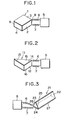
- Fig. 1 illustrates an electro-optical element 1 of a rectangular body according to a first embodiment, in which p-nitroaniline is used as the low molecular weight compound showing an electro-optical effect and polymethylmethacrylate is used as the thermoplastic resin.
- An electro-optical resin layer 2 is composed of a resin composition melt formed by homogeneously mixing these materials in a weight ratio of 2:8 and finished by chemically polishing the surfaces. Electrodes 3 and 4 are attached to the opposite surfaces (surfaces of for example 5 x 3 mm 2 ) of the electro-optical resin layer 2 having a rectangular body shape of a size of for example 5 mm x 3 mm x 2 mm.
- Wires 6 and 7 extending from a power source 5 are connected to the electrodes 3 and 4, respectively.
- This element 1 shows a Kerr constant of 1.7 x 10 -10 cm/v 2 when light enters one of a pair of opossite surfaces (for instance, surfaces 8 and 9 of 2 x 3 mm 2 ) on which no electrodes are provided, and light leaves the opposite surface.
- Fig. 2 illustrates an electro-optical element 11 according to a second embodiment, in which an electro-optical resin composition 12 is of right-angled prism shape, having two converging sides 13 and 14 of for example 5 mm length and 2 mm width and having electrodes 15 and 16 attached to opposite parallel surfaces, as shown.
- an electro-optical resin composition 12 is of right-angled prism shape, having two converging sides 13 and 14 of for example 5 mm length and 2 mm width and having electrodes 15 and 16 attached to opposite parallel surfaces, as shown.
- F ig. 3 illustrates an electro-optical element 21 according to a third embodiment.
- the electro-optical composition 22 is of regular traiangular prism shape having sides 23, 24 and 25 of 3 mm and an axial length of 10 mm.
- a pair of independent electrodes 26 and 27 are attached to the two adjacent sides 23 and .24.
- F ig. 4 illustrates an electro-optical element 31 according to a fourth embodiment, in the form of a film.
- the electro-optical resin composition film 32 has electrodes 33 and 34 on its surfaces. Further, one or both of the electrodes 33 and 34 may be constructed from a transparent conductive foil such as ITO (indium oxide-tin) .
- ITO indium oxide-tin
- the electro-optical elements 1, 11, 21 and 31 illustrated in Figs. 1 to 4 are useful as elements for light intensity modulating apparatus and light deflecting apparatus in the same manner as conventional electro-optical elements.
- the electro-optical element 1 of Fig. 1 can be incorporated in a light intensity modulating apparatus as shown in Fig. 5.
- the element 1 with the electrodes 3 and 4 connected to the power source 5 via wires 6 and 7, is arranged so that the surface by which light enters is at right angles to the path of polarized light from a light source 37 passing through a polarizer 38, in order to avoid refraction of the light.
- the light passed through the electro-optical resin layer 2 passes through an analyzer 39 and is received by a light receiving element 40 disposed therebehind.
- the quantity of the light photoelectrically converted by the light receiving element 40 is recorded on a recorder 41 as an electric signal. Firstly, light is passed whilst no voltage is applied to the element 1, and the polarizer 38 and the analyzer 39 are set to cross at a right angle, to minimize the light passing through the analyzer 39. Then a voltage is applied across the electrodes 3 and 4, and the intensity of the light passing through the analyzer 39 is modulated to become greater as a result of a change in the retardation of the light passing through the element 1.
- the element 1 serves as a means for controlling the intensity of the light.
- a signal wave is obtainable in which the brightness changes correspond to the cycle of the alternating current.
- the electrodes 33 and 34 are made of a transparent material and the element 31 is arranged at an inclination to the light path so that the light passed through one of the electrodes 33 or 34 passes obliquely through the electro-optical resin layer 31 ar:d goes out through the other electrode 34 or 33, whereby, in the same manner as in the above case, the retardation of the light passing through the element 31 changes due to the voltage applied to the electrodes 33 and 34 and the light intensity can thereby be modulated.
- the electrode 34 is made of an opaque material which reflects light
- the light entering the transparent electrode 33 passes through the electro-optical resin layer 32, is reflected by the opaque electrode 34, passes again through the resin layer 32 and goes out through the transparent electrode 33.
- the analyzer 39 and the light receiving element 40 are disposed in the light path of the reflected light, the light ntensity can be modulated in the same manner as in the above case.
- the incoming light is not at a right angle to the film surface, as is the case here
- there is a tendency for the light to undergo refraction in the film and light deflection, caused by the electro-optical effect occurs.
- the change of the angle is minimal and it is usually possible to carry out substantially only the light intensity modulation.
- the electro-optical elements 11 and 21 of Figs. 2 and 3 can also be used for light intensity modulation. However, these elements 11 and 21 are particularly suitable for use as light deflecting elements (in certain cases, the element 1 of Fig. 1 is also useful as a light deflecting element.) Their practical applications will be described with respect to the light deflecting apparatus shown in Figs. 6 and 7.
- the light from a light source 44 is polarized by a polarizer 45, then enters one of the surfaces of the prism shaped element 11 of Fig. 2 on which there are no electrodes, passes obliquely through the electro-optical resin layer 12 and goes out through the opposite surface.
- the light path is shown in Fig. 6B, in which the point at which the light enters the element 11 is designated by A, the outlet of the light when voltage is applied to the electrodes 15 and 16 is designated by B, and the direction of the out-going light is designated by BC.
- the refractive index to the polarized light changes, and as a result, the light entering at point A goes out from point D, as illustrated by the dotted line in Fig. 6B, and the out-going light travels in the direction DE. That is, the light BC is deflected to become the light following the path DE.
- Fig. 7 illustrates a case wherein light passed through a polarized similar to the one shown in Fig. 6, is passed through the element 21 of Fig. 3 for deflection. That is, as shown by Figs. 7A and 7B, light entering from point A' passes obliquely through the triangular prism shape element 21, reaches point B' and goes out in the direction B'C', when no electric field is applied. In this element 21, the nearer the electrodes 26 and 27 are to one of the apexes of the triangle, the closer they become to each other.
- the change in the refractive index of the resin near the point A' due to the electro-optical effect is minimal, and as the electrodes 26 and 27 are. closer the point B', a change in the refractive index due to the electro-optical effect increases towards the point B'. Accordingly, the light passing through the element 21 is arcuately deflected towards the point where the refractive index is greater, as shown by the dotted line in Fig. 7B, as viewed from above the element 21, and the out-going light is deflected in the direction shown by D'E'.
- a trianglular flat plate shaped element 11 and a triangular prism shaped element 21 are used, respectively.
- these elements need not necessarily be of triangular shape, and they may take any other polygonal shape.
- p-nitroaniline was chosen, and as a polymer substance, polymethylmethacrylate was selected.
- p-nitroaniline and polymethylmethacrylate were mixed in weight ratios of (1) 10:90 and (2) 20:80, respectively.
- Each mixture was dissolved in acetone, and well dispersed and mixed, and the solvent acetone was removed from the liquid thus obtained, with care not to cause foaming, whereupon solid compositions having weight ratios of p-nitroaniline to polymethylmethacrylate of (1) 1 0 :90 and (2) 20:80, respectively, were obtained.
- These compositions were transparent yellowish substances.
- the solid compositions thus prepared were melt formed, and then optically polished, whereupon electro-optical units 2 having a rectangular body shape of 5 x 3 mm x 2 mm as shown in Fig. 1 were obtained. Electrodes 3 and 4 were attached, respectively, to opposite surfaces of 5 mm x 3 mm of each electro-optical unit 2, to obtain a sample 1 for measuring an electro-optical effect. With use of the samples 1 thus obtained, their double refractive indexes were measured by means of the measuring system shown in Fig. 8. In this measuring system as in the case of Fig.
- reference numeral 5 designates a direct current power source
- numeral 37 designates a He-Ne laser light source
- numerals 38 and 39 designate a polarizer and an analyzer, respectively, which are arranged to cross at a right angle to each other.
- Reference numeral 42 is a Babinet-Soleil's compensator
- numeral 40 designates a photo-diode. The quantity of the light detected after being photo-electrically converted by the photo-diode, is recorded on a recorder 41 as an electric signal.
- the measurement was conducted in the following manner. Firstly, the light beam entering the sample 1 from the polarizer 38 was led in parallel with the electrodes 3, 4 attached to the electro-optical element 2 of the sample 1, and the Babinet-Soleil's compensator 42 was adjusted to minimize the light entering the photodiode 40. Then, when a direct current voltage was applied to the sample 1, the double refractive index of the electro-optical material 2 changed due to the electro-optical effect and as a result, the intensity of light entering the photo-diode 40 increased. The Babinet-Soleil's compensator 42 was adjusted to minimize the increased light intensity and from the reading of the micrometer of the Baninet-Soleil's compensator 42, the change in the double refractive index was measured.
- nitro aromatic compounds As nitro aromatic compounds, (a) p-nitroaniline, (b) o-nitroaniline, (c) 2-nitro-4-methoxyaniline, (d) p-nitro-o-chloroaniline, (e) 5-nitro-o-toluidine, (f) 2-nitro-diphenylamine, (g) l,2-diamino-4-nitrobenzene and (h) p-nitrophenol, were chosen and as a polymer substance, polymethylmethacrylate was selected.
- Each of the polar substances (a) to (h), showing electro-optical effects, and polymethylmethacrylate were mixed in a weight ratio of 10:90.
- Each mixture thereby obtained was dissolved in acetone in a manner similar to Example 1, whereby a molten liquid mixture was obtained.
- Each liquid mixture was cast on a glass with a transparent metal oxide electrode thereon and the solvent was carefully evaporated, whereupon an optically homogeneous cast film was obtained. Further, a ITO transparent electrode was vapour deposited on the cast film, and electrode lead wires were taken out from the glass on the metal oxide electrode side and on the vapour- deposited ITO electrode side, to form a sample for measurement of the electro-optical effect.
- the thickness of the films were (a) 100 ⁇ , (b) 230 ⁇ , (c) 190 ⁇ , (d) 180 ⁇ , (e) 250 ) ⁇ , (f) 250 ⁇ , (g) 230 ⁇ , and (h) 220 ⁇ .
- the Kerr constants of the respective films were as follows: (a) p-nitroaniline: 2.7 x 10 - 12 cm/V 2 , (b) o-nitroaniline: 2 x 10 -12 cm/V 2 , (c) 2-nitro-4-methoxyaniline: 2.1 x 10 -12 cm/v2, ( d ) p-nitro-o-chloroaniline: 4.0 x 10 -12 cm/V2, (e) 5-nitro-o-toluidine: 4.4 x 10 -12 cm/V 2 , (f) 2-nitro-diphenylamine: 1.1 x 10 12 cm/V 2 , (g) 1,2-diamino-4-nitrobenzene: 4:1 x 10 -12 cm/V 2 and (h) p-nitro
- nitro aromatic compound p-nitroaniline was chosen, and as a polymer substance, polyvinylacetate was selected. They were mixed in a weight ratio of 10:90. Cast films having thicknesses of 130 ⁇ . and 310 ⁇ were prepared on glass with a metal oxide electrode in the same manner as in Example 2. The electro-optical effects of these films were measured in the same manner as in Example 2, whereupon it was found that their Kerr constants were 8.0 x 10 -12 cm/V 2 and 19 x 10 -12 cm/V 2 , respectively .
- the electro-optical materials having electro-optical effects according to the present invention are optically uniform, show no double refraction and are easier to form. Thus, they are extremely useful as materials for dynamic optical products.
Landscapes
- Physics & Mathematics (AREA)
- Nonlinear Science (AREA)
- General Physics & Mathematics (AREA)
- Optics & Photonics (AREA)
- Compositions Of Macromolecular Compounds (AREA)
Applications Claiming Priority (4)
| Application Number | Priority Date | Filing Date | Title |
|---|---|---|---|
| JP12019680A JPS5745519A (en) | 1980-08-30 | 1980-08-30 | Electrooptic material |
| JP120196/80 | 1980-08-30 | ||
| JP131827/80 | 1980-09-22 | ||
| JP55131827A JPS5756816A (en) | 1980-09-22 | 1980-09-22 | Electrooptic element |
Publications (2)
| Publication Number | Publication Date |
|---|---|
| EP0047162A1 true EP0047162A1 (fr) | 1982-03-10 |
| EP0047162B1 EP0047162B1 (fr) | 1986-05-14 |
Family
ID=26457814
Family Applications (1)
| Application Number | Title | Priority Date | Filing Date |
|---|---|---|---|
| EP81303963A Expired EP0047162B1 (fr) | 1980-08-30 | 1981-08-28 | Elément électro-optique à effet Kerr |
Country Status (3)
| Country | Link |
|---|---|
| US (1) | US4428873A (fr) |
| EP (1) | EP0047162B1 (fr) |
| DE (1) | DE3174628D1 (fr) |
Cited By (5)
| Publication number | Priority date | Publication date | Assignee | Title |
|---|---|---|---|---|
| EP0282963A2 (fr) * | 1987-03-16 | 1988-09-21 | Hoechst Celanese Corporation | Composite polymère microdispersé/cristal liquide |
| EP0295145A2 (fr) * | 1987-06-11 | 1988-12-14 | Canon Kabushiki Kaisha | Méthode et appareil d'enregistrement |
| EP0306359A2 (fr) * | 1987-07-31 | 1989-03-08 | Schlumberger Industries | Dispositif pour un test d'un circuit |
| EP0453362A1 (fr) * | 1990-04-19 | 1991-10-23 | Commissariat A L'energie Atomique | Dispositif de traitement d'hologrammes dynamiques utilisant un film mince polymérique à caractère photoréfractif |
| US5272434A (en) * | 1987-06-20 | 1993-12-21 | Schlumberger Technologies, Inc. | Method and apparatus for electro-optically testing circuits |
Families Citing this family (25)
| Publication number | Priority date | Publication date | Assignee | Title |
|---|---|---|---|---|
| US4939388A (en) * | 1985-05-10 | 1990-07-03 | E. I. Du Pont De Nemours And Company | Second harmonic generation by inclusion complexes of cyclodextrin compounds |
| US4707303A (en) * | 1985-06-25 | 1987-11-17 | Celanese Corporation | High performance nonlinear optical substrates |
| US4983325A (en) * | 1985-06-25 | 1991-01-08 | Hoechst Celanese Corp. | High performance nonlinear optical media |
| US4717508A (en) * | 1985-09-03 | 1988-01-05 | Hoechst Celanese Corporation | Organic nonlinear optical substrates |
| US4720355A (en) * | 1985-09-03 | 1988-01-19 | Hoechst Celanese Corporation | Organic nonlinear optical substrates |
| US4859876A (en) * | 1985-09-16 | 1989-08-22 | AT&T Bell Laboratories American Telephone and Telegraph Company | Nonlinear optical materials and devices |
| US4767195A (en) * | 1986-03-21 | 1988-08-30 | Hughes Aircraft Company | System and method for encoding information onto an optical beam |
| US4869579A (en) * | 1986-07-31 | 1989-09-26 | Technion Research & Development Foundation | Optical apparatus and method for beam coupling useful in light beam steering and spatial light modulation |
| DK449286A (da) * | 1986-09-19 | 1988-03-20 | Nordiske Kabel Traad | Fremgangsmaade til fremstilling af et elektrooptisk materiale med styrbare optiske egenskaber samt anvendelse af materialet i elektrooptiske komponenter |
| JPH0721512B2 (ja) * | 1987-03-27 | 1995-03-08 | 日本碍子株式会社 | 光センサ用光部品 |
| JPS648514A (en) * | 1987-07-01 | 1989-01-12 | Canon Kk | Method and device for reproducing optical information and optical information recording medium |
| US4981614A (en) * | 1987-09-21 | 1991-01-01 | Canon Kabushiki Kaisha | Solid solution |
| JPH0193718A (ja) * | 1987-10-06 | 1989-04-12 | Murata Mfg Co Ltd | 光変調器 |
| US4941996A (en) * | 1987-10-19 | 1990-07-17 | Minnesota Mining And Manufacturing Company | Inclusion complexes providing second harmonic generation |
| DE68919717T2 (de) * | 1988-01-27 | 1995-05-18 | Nippon Telegraph & Telephone | Organisches Material mit nichtlinearen optischen Eigenschaften und Vorrichtung mit nichtlinearen optischen Eigenschaften. |
| US4867540A (en) * | 1988-02-16 | 1989-09-19 | Hoechst Celanese Corp. | Condensation polymers exhibiting nonlinear optical response |
| EP0362839A1 (fr) * | 1988-10-05 | 1990-04-11 | Sumitomo Electric Industries, Ltd. | Unité d'affichage |
| US4985178A (en) * | 1988-11-22 | 1991-01-15 | E. I. Du Pont De Nemours And Company | Nonlinear optical device from 3-methyl-4-methoxy-4'-nitrostilbene |
| US5255428A (en) * | 1991-04-03 | 1993-10-26 | California Institute Of Technology | Electrooptic polymer voltage sensor and method of manufacture thereof |
| US5200107A (en) * | 1991-08-26 | 1993-04-06 | Aristech Chemical Corporation | Polymethylmethacrylate syrup as medium for liquid crystals |
| US6137619A (en) * | 1998-04-08 | 2000-10-24 | Nz Applied Technologies, Incorporated | High-speed electro-optic modulator |
| US6404537B1 (en) | 2000-03-06 | 2002-06-11 | Corning Applied Technologies Corporation | Polarization transformer |
| JP4994826B2 (ja) * | 2006-12-25 | 2012-08-08 | オリンパス株式会社 | レーザ顕微鏡 |
| EP2231058B1 (fr) * | 2007-12-19 | 2017-05-10 | 3M Innovative Properties Company | Emballage dentaire, et procédé de distribution d'un matériau dentaire depuis un emballage |
| US11009662B2 (en) * | 2017-09-05 | 2021-05-18 | Facebook Technologies, Llc | Manufacturing a graded index profile for waveguide display applications |
Citations (5)
| Publication number | Priority date | Publication date | Assignee | Title |
|---|---|---|---|---|
| US3215038A (en) * | 1961-11-15 | 1965-11-02 | Ibm | Solid solution electro-optic light switch using the stark effect |
| CH469994A (de) * | 1966-04-12 | 1969-03-15 | Inst Kristallografii An Sssr | Vorrichtung zur Ablenkung eines Lichtbündels |
| US3813265A (en) * | 1970-02-16 | 1974-05-28 | A Marks | Electro-optical dipolar material |
| DE2719483A1 (de) * | 1976-05-03 | 1977-11-24 | Eastman Kodak Co | Elektrooptische einrichtung |
| DE2839103A1 (de) * | 1978-09-08 | 1980-03-20 | Research Frontiers Inc | Suspension fuer lichtventile und verfahren zur herstellung |
-
1981
- 1981-08-27 US US06/297,016 patent/US4428873A/en not_active Expired - Fee Related
- 1981-08-28 DE DE8181303963T patent/DE3174628D1/de not_active Expired
- 1981-08-28 EP EP81303963A patent/EP0047162B1/fr not_active Expired
Patent Citations (5)
| Publication number | Priority date | Publication date | Assignee | Title |
|---|---|---|---|---|
| US3215038A (en) * | 1961-11-15 | 1965-11-02 | Ibm | Solid solution electro-optic light switch using the stark effect |
| CH469994A (de) * | 1966-04-12 | 1969-03-15 | Inst Kristallografii An Sssr | Vorrichtung zur Ablenkung eines Lichtbündels |
| US3813265A (en) * | 1970-02-16 | 1974-05-28 | A Marks | Electro-optical dipolar material |
| DE2719483A1 (de) * | 1976-05-03 | 1977-11-24 | Eastman Kodak Co | Elektrooptische einrichtung |
| DE2839103A1 (de) * | 1978-09-08 | 1980-03-20 | Research Frontiers Inc | Suspension fuer lichtventile und verfahren zur herstellung |
Cited By (9)
| Publication number | Priority date | Publication date | Assignee | Title |
|---|---|---|---|---|
| EP0282963A2 (fr) * | 1987-03-16 | 1988-09-21 | Hoechst Celanese Corporation | Composite polymère microdispersé/cristal liquide |
| EP0282963A3 (en) * | 1987-03-16 | 1990-07-18 | Hoechst Celanese Corporation | A microdisperse polymer/liquid crystal composite |
| EP0295145A2 (fr) * | 1987-06-11 | 1988-12-14 | Canon Kabushiki Kaisha | Méthode et appareil d'enregistrement |
| EP0295145B1 (fr) * | 1987-06-11 | 1996-04-10 | Canon Kabushiki Kaisha | Méthode et appareil d'enregistrement |
| US5272434A (en) * | 1987-06-20 | 1993-12-21 | Schlumberger Technologies, Inc. | Method and apparatus for electro-optically testing circuits |
| EP0306359A2 (fr) * | 1987-07-31 | 1989-03-08 | Schlumberger Industries | Dispositif pour un test d'un circuit |
| EP0306359A3 (en) * | 1987-07-31 | 1990-12-19 | Schlumberger Industries | Device for testing a circuit |
| US5394098A (en) * | 1987-07-31 | 1995-02-28 | Schlumberger Technologies, Inc. | Apparatus including electro-optical material for use in testing a circuit having voltage-bearing elements proximate a surface of a body |
| EP0453362A1 (fr) * | 1990-04-19 | 1991-10-23 | Commissariat A L'energie Atomique | Dispositif de traitement d'hologrammes dynamiques utilisant un film mince polymérique à caractère photoréfractif |
Also Published As
| Publication number | Publication date |
|---|---|
| DE3174628D1 (en) | 1986-06-19 |
| EP0047162B1 (fr) | 1986-05-14 |
| US4428873A (en) | 1984-01-31 |
Similar Documents
| Publication | Publication Date | Title |
|---|---|---|
| EP0047162A1 (fr) | Elément électro-optique à effet Kerr | |
| Yamada et al. | Electric‐field induced cylindrical lens, switching and deflection devices composed of the inverted domains in LiNbO3 crystals | |
| Nose et al. | A liquid crystal microlens obtained with a non-uniform electric field | |
| Carter et al. | Nonlinear Optical Properties of Organic Polymer Materials | |
| US4958895A (en) | Optical waveguides | |
| US4201442A (en) | Liquid crystal switching coupler matrix | |
| US4887884A (en) | Capillary non-linear optical waveguide device | |
| EP0488708B1 (fr) | Dispositif de commutation optique | |
| DE2855841A1 (de) | Optische fokussiereinrichtung mit variabler brennweite | |
| US6093344A (en) | Polymer dispersed liquid crystal display device | |
| US3980395A (en) | Liquid crystal switch for optical waveguide | |
| US5172257A (en) | Twisted ferroelectric liquid crystal modulator for providing gray scale | |
| CA2039060C (fr) | Dispositifs optiques non lineaires | |
| Simoni et al. | Optical nonlinearities induced by thermal effects in polymer dispersed liquid crystals | |
| EP0624812B1 (fr) | Dispositif de modulation de la lumière à cristal liquide | |
| DE2408389A1 (de) | Elekkrooptisches verfahren unter verwendung von fluessigkristallen | |
| Cipparrone et al. | Nonlinear optical effects in polymer dispersed liquid crystals | |
| Nose | Optical properties of a liquid crystal microlens | |
| US4985179A (en) | Optical material | |
| Nazarenko et al. | Unipolar electro-optic effect in a nematic cell | |
| US5889907A (en) | Optical processing method using fine liquid crystal droplets and waveguide type optical device for optical processing | |
| Sugiyama et al. | Growth and photoreactive properties of a-and c-axis cerium-doped strontium barium niobate single-crystal fibers | |
| JPS6248811B2 (fr) | ||
| Nose et al. | Application of a liquid crystal microlens to an optical fiber switch | |
| US5093882A (en) | Wavelength conversion device |
Legal Events
| Date | Code | Title | Description |
|---|---|---|---|
| PUAI | Public reference made under article 153(3) epc to a published international application that has entered the european phase |
Free format text: ORIGINAL CODE: 0009012 |
|
| AK | Designated contracting states |
Designated state(s): DE FR GB NL |
|
| 17P | Request for examination filed |
Effective date: 19820708 |
|
| GRAA | (expected) grant |
Free format text: ORIGINAL CODE: 0009210 |
|
| AK | Designated contracting states |
Kind code of ref document: B1 Designated state(s): DE FR GB NL |
|
| REF | Corresponds to: |
Ref document number: 3174628 Country of ref document: DE Date of ref document: 19860619 |
|
| ET | Fr: translation filed | ||
| PLBE | No opposition filed within time limit |
Free format text: ORIGINAL CODE: 0009261 |
|
| STAA | Information on the status of an ep patent application or granted ep patent |
Free format text: STATUS: NO OPPOSITION FILED WITHIN TIME LIMIT |
|
| 26N | No opposition filed | ||
| PGFP | Annual fee paid to national office [announced via postgrant information from national office to epo] |
Ref country code: FR Payment date: 19900807 Year of fee payment: 10 |
|
| PGFP | Annual fee paid to national office [announced via postgrant information from national office to epo] |
Ref country code: GB Payment date: 19900820 Year of fee payment: 10 |
|
| PGFP | Annual fee paid to national office [announced via postgrant information from national office to epo] |
Ref country code: NL Payment date: 19900831 Year of fee payment: 10 |
|
| PGFP | Annual fee paid to national office [announced via postgrant information from national office to epo] |
Ref country code: DE Payment date: 19900927 Year of fee payment: 10 |
|
| PG25 | Lapsed in a contracting state [announced via postgrant information from national office to epo] |
Ref country code: GB Effective date: 19910828 |
|
| PG25 | Lapsed in a contracting state [announced via postgrant information from national office to epo] |
Ref country code: NL Effective date: 19920301 |
|
| NLV4 | Nl: lapsed or anulled due to non-payment of the annual fee | ||
| GBPC | Gb: european patent ceased through non-payment of renewal fee | ||
| PG25 | Lapsed in a contracting state [announced via postgrant information from national office to epo] |
Ref country code: FR Effective date: 19920430 |
|
| PG25 | Lapsed in a contracting state [announced via postgrant information from national office to epo] |
Ref country code: DE Effective date: 19920501 |
|
| REG | Reference to a national code |
Ref country code: FR Ref legal event code: ST |