EP0045891A2 - Hochleistungseinrichtung zum Überspannungsschutz - Google Patents
Hochleistungseinrichtung zum Überspannungsschutz Download PDFInfo
- Publication number
- EP0045891A2 EP0045891A2 EP81105904A EP81105904A EP0045891A2 EP 0045891 A2 EP0045891 A2 EP 0045891A2 EP 81105904 A EP81105904 A EP 81105904A EP 81105904 A EP81105904 A EP 81105904A EP 0045891 A2 EP0045891 A2 EP 0045891A2
- Authority
- EP
- European Patent Office
- Prior art keywords
- carbide
- junction
- assembly
- binder
- particulate
- Prior art date
- Legal status (The legal status is an assumption and is not a legal conclusion. Google has not performed a legal analysis and makes no representation as to the accuracy of the status listed.)
- Withdrawn
Links
Images
Classifications
-
- H—ELECTRICITY
- H01—ELECTRIC ELEMENTS
- H01C—RESISTORS
- H01C7/00—Non-adjustable resistors formed as one or more layers or coatings; Non-adjustable resistors made from powdered conducting material or powdered semi-conducting material with or without insulating material
- H01C7/10—Non-adjustable resistors formed as one or more layers or coatings; Non-adjustable resistors made from powdered conducting material or powdered semi-conducting material with or without insulating material voltage responsive, i.e. varistors
- H01C7/105—Varistor cores
- H01C7/118—Carbide, e.g. SiC type
-
- H—ELECTRICITY
- H01—ELECTRIC ELEMENTS
- H01C—RESISTORS
- H01C7/00—Non-adjustable resistors formed as one or more layers or coatings; Non-adjustable resistors made from powdered conducting material or powdered semi-conducting material with or without insulating material
- H01C7/10—Non-adjustable resistors formed as one or more layers or coatings; Non-adjustable resistors made from powdered conducting material or powdered semi-conducting material with or without insulating material voltage responsive, i.e. varistors
- H01C7/12—Overvoltage protection resistors
-
- H—ELECTRICITY
- H01—ELECTRIC ELEMENTS
- H01C—RESISTORS
- H01C7/00—Non-adjustable resistors formed as one or more layers or coatings; Non-adjustable resistors made from powdered conducting material or powdered semi-conducting material with or without insulating material
- H01C7/13—Non-adjustable resistors formed as one or more layers or coatings; Non-adjustable resistors made from powdered conducting material or powdered semi-conducting material with or without insulating material current responsive
-
- H—ELECTRICITY
- H01—ELECTRIC ELEMENTS
- H01L—SEMICONDUCTOR DEVICES NOT COVERED BY CLASS H10
- H01L2924/00—Indexing scheme for arrangements or methods for connecting or disconnecting semiconductor or solid-state bodies as covered by H01L24/00
- H01L2924/0001—Technical content checked by a classifier
- H01L2924/0002—Not covered by any one of groups H01L24/00, H01L24/00 and H01L2224/00
Definitions
- High voltage diodes e.g., silicon rectifiers are used today in many applications such as in switching and non-switching power supplies as well as part of a rectifier bridge. These diodes are relatively expensive in the first instance and since they are often subject to high voltage over-voltage (e.g., reverse surges) they are liable to burn out due to the over-voltage causing reverse voltage junction breakdown. This obviously requires repair of the power supply which is quite costly as well as the replacement of the burned out diode.
- the above identified over-voltage breakdown is also a problem encountered by semiconductor devices such as silicon-controlled rectifiers, and transistors e.g., mos-fets as well as other semiconductor junction devices. Over-voltage protection is also needed in a variety of other applications wherever overload voltages are apt to occur e.g., between conductors and conductors to ground of circuit boards, between an insulated pipe junction used for gas or oil transmission and etc.
- the present invention provides a material which will function to protect components or equipment against destructive over-voltages.
- This disclosure concerns an over-voltage protection material and its use in providing overvoltage protection.
- the material functions at threshold breakdown voltage to effectively limit the voltage across the component, equipment or etc. being protected by bypassing or shunting the damaging current produced by the overvoltage.
- the material is selected to have a threshold conduction voltage less than the reverse breakdown voltage of a component such as a diode, transistor, etc. being protected.
- a threshold voltage breakdown material containing silicon carbide particles (powder) and a lesser amount by volume of a Group IV B element - carbide particles (powder) in a dielectric plastic binder will have a significantly lower breakdown voltage than that achievable using silicon carbide particles alone.
- the addition of Group IV B element-carbide particles does not significantly effect the important non linear voltage breakdown characteristics in comparison with the use of silicon carbide particles alone.
- Group IV B elements are: Titantium (Ti), Zirconium (Zr), and Hafnium (Hf) as shown in the text "University Chemistry” Bailar et al, D. C. Heath & Company, Boston, MA, copyright 1965, Library of Congress card No. 65-11347.
- the package may take many shapes, e.g., see the brochures put out by various manufacturers of rectifiers. Since the invention does not reside in the diode rectifier itself, or its construction, it will not be discussed in any further detail.
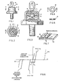
- Figs. 4 and 5 there is shown the voltage threshold material 16 preformed in the shape of a washer so that it may be placed in the assembly as shown in Figs.2 and 3.
- Fig. 3 illustrates the material 16 (as a washer) between an inner electrode 17 and outer metal case 12 of the assembly.
- the washer is selected such that its outer diameter is larger than the inner diameter of the case 12 and its inner diemeter is less than the outer diameter of the electrode 17 in contact therewith, so that it fits tightly (squeezed) to make good electrical and physical contactwith the parts with which it is in contact.
- the electrode 16 is electrically coupled to wire 13 by soldering or conducting adhesive or electrode 17 and wire 13 may be one piece. •
- the material 16 will rapidly breakdown in a time believed to be less than junction breakdown time and occurs at a lower voltage than the reverse breakdown voltage of the junction.
- a potting compound 15, e.g., epoxy or glass is used to effect a hermatic seal.
- a terminator lug 18 is crimped to make contact with the electrode narrow portion 17 - 1.
- shapes other than a washer may be used for the material 16 depending upon the application and packaging, e.g., rings, grommet.
- a plastic binder e.g., a rubber
- a curing agent mechanical reinforcement particles, e.g., silica are mixed with silicon carbide particles and Group IV B element-carbide particles.
- the mixture is then worked on a roll mill to homogeneously mix (uniformly disperse) the silicon carbide and Group IV B element-carbide particles and silica in the rubber and it is then sheeted out.
- the preferred Group IV B element-carbide particles are Titatium carbide particles and the preferred plastic is silicone gum.
- Suitable plastics may include elastomers and non-elastomers depending upon the application.
- Suitable plastice (the term as'used herein meant to include rubber and other elastomers thermosetting plastics, and thermoplastics) includes e.g., silicone rubber, fluorosilicone rubbers, chloroinated or chlorosulphonated polyethylene, polyethylene, polybutylene, polypropylene, ethycellulose, polyamide, natural rubber, SBR, neoprene, nitrile rubber, butyl rubber, epoxy and polyurethane rubber.
- the sheet is cured in a press and the washer or other configuration as needed is punched out or die cut therefrom.
- the washer or sheet can be molded if desired or the material 16 may be made in situ using a potting composition of the material chich cures in place.
- the parameters of cure can obviously change, however it is preferred that if rubber is selected it have about a 4 to 4.5% shrinkage on cure to increase the volume loading of the particles in the form stable material 16.
- a suitable formulation for making the low voltage breakdown of threshold material 16 comprises a base (binder) mixture of:
- the binder mixture is about 60% by volume of the above material 1( I with the silicone gum being about 50.74 Vol. percent.
- the sheet thickness may obviously be varied depending upon requirements, however a thickness of 10 mils to 400 mils may be conveniently made. At this time the sheet is die cut to provide the washer 16.
- the above provides a material 16 having a bidirectional threshold conduction of less than about 25 - 50 volts. It should be understood that the invention herein is applicable to at least silicon and germanium semiconductor junction devices.
- the sheet be loaded such that about 20-35 percent by Vol. of silicon carbide is used and 5-20 percent by Vol. of Group IV B element-carbide particles is used e.g., titanium carbide, zirconium carbide, and etc.
- This provides a preferred volume loading of about 25 to 55% of 1 particles as used herein volume loading is calculated based on the total of plastic binder + SiC particles and Group IV B element-carbide particles.
- Silicon carbide particles and the Group IV B element-carbide e.g. titanium carbide, zirconium carbide, hafnium carbide particles are preferably selected so that they have an average particle size of between 75 microns to about 3 microns.
- the threshold conduction voltage of the material may be varied depending upon the requirement, however it may be conveniently between about 1000 to 25 volts (+ or -) since this meets the requirements of most high voltage power diodes as well as lower voltage applications.
- Fig. 6 there is shown the typical reverse breakdown voltage curve of a semiconductor junction and the typical threshold conduction voltage for the material 16 if made with SiC + TiC.
- the threshold conduction voltage of the material 16 will obviously be adjusted by adjusting the particle loading to insure threshold conduction of the material is set high enough so that negative and positive voltages normally encountered will not cause it to conduct significantly.
- the dashed curve illustrates the characteristics if made only with equal loading of S iC particles.
- a comparison between the curves illustrates the significant decrease in threshold conduction with the present invention.
- a piece 29 of threshold conduction sheet material coupled e.g., by electrically conductive adhesive between or across circuit pattern lines 31 and 32 (e.g., copper or electrically conductive ink) on a conventional dielectric e.g., plastic circuit board 30.
- circuit pattern lines 31 and 32 e.g., copper or electrically conductive ink
- dielectric e.g., plastic circuit board 30 e.g., copper or electrically conductive ink
Applications Claiming Priority (2)
| Application Number | Priority Date | Filing Date | Title |
|---|---|---|---|
| US06/177,648 US4331948A (en) | 1980-08-13 | 1980-08-13 | High powered over-voltage protection |
| US177648 | 2002-06-20 |
Publications (2)
| Publication Number | Publication Date |
|---|---|
| EP0045891A2 true EP0045891A2 (de) | 1982-02-17 |
| EP0045891A3 EP0045891A3 (de) | 1983-04-27 |
Family
ID=22649400
Family Applications (1)
| Application Number | Title | Priority Date | Filing Date |
|---|---|---|---|
| EP81105904A Withdrawn EP0045891A3 (de) | 1980-08-13 | 1981-07-27 | Hochleistungseinrichtung zum Überspannungsschutz |
Country Status (5)
| Country | Link |
|---|---|
| US (1) | US4331948A (de) |
| EP (1) | EP0045891A3 (de) |
| JP (1) | JPS5758357A (de) |
| CA (1) | CA1167908A (de) |
| DK (1) | DK340381A (de) |
Cited By (3)
| Publication number | Priority date | Publication date | Assignee | Title |
|---|---|---|---|---|
| FR2527039A1 (fr) * | 1982-05-14 | 1983-11-18 | Inf Milit Spatiale Aeronaut | Dispositif de protection d'un dispositif electronique contre les tensions engendrees par un champ electromagnetique |
| EP0228983A2 (de) * | 1985-12-02 | 1987-07-15 | Emerson Electric Co. | Hermetisch verschlossener Batteriedeckel |
| EP0369826A2 (de) * | 1988-11-18 | 1990-05-23 | G & H Technology, Inc. | Werkstoffzusammensetzung zur Verwendung in einem elektrischen Überspannungsimpulsschutz und Verfahren zu deren Herstellung |
Families Citing this family (59)
| Publication number | Priority date | Publication date | Assignee | Title |
|---|---|---|---|---|
| US4726991A (en) * | 1986-07-10 | 1988-02-23 | Eos Technologies Inc. | Electrical overstress protection material and process |
| US4977357A (en) * | 1988-01-11 | 1990-12-11 | Shrier Karen P | Overvoltage protection device and material |
| US5260848A (en) * | 1990-07-27 | 1993-11-09 | Electromer Corporation | Foldback switching material and devices |
| US5142263A (en) * | 1991-02-13 | 1992-08-25 | Electromer Corporation | Surface mount device with overvoltage protection feature |
| US5248517A (en) * | 1991-11-15 | 1993-09-28 | Electromer Corporation | Paintable/coatable overvoltage protection material and devices made therefrom |
| US5294374A (en) * | 1992-03-20 | 1994-03-15 | Leviton Manufacturing Co., Inc. | Electrical overstress materials and method of manufacture |
| US5246388A (en) * | 1992-06-30 | 1993-09-21 | Amp Incorporated | Electrical over stress device and connector |
| EP0589560B1 (de) * | 1992-09-23 | 1997-10-22 | The Whitaker Corporation | Vorrichtung zum Schutz gegen elektrische Überbeanspruchung |
| US5277625A (en) * | 1992-11-03 | 1994-01-11 | The Whitaker Corporation | Electrical connector with tape filter |
| US5409401A (en) * | 1992-11-03 | 1995-04-25 | The Whitaker Corporation | Filtered connector |
| US5269705A (en) * | 1992-11-03 | 1993-12-14 | The Whitaker Corporation | Tape filter and method of applying same to an electrical connector |
| US6191928B1 (en) | 1994-05-27 | 2001-02-20 | Littelfuse, Inc. | Surface-mountable device for protection against electrostatic damage to electronic components |
| BR9508404A (pt) | 1994-07-14 | 1997-11-25 | Surgx Corp | Componente de proteção de voltagem variável e processo de produção do mesmo |
| US5991137A (en) * | 1996-02-20 | 1999-11-23 | General Electric Company | Partial discharge coupler |
| US6285538B1 (en) | 1996-02-20 | 2001-09-04 | General Electric Company | Partial discharge coupler |
| US6251513B1 (en) | 1997-11-08 | 2001-06-26 | Littlefuse, Inc. | Polymer composites for overvoltage protection |
| TW511103B (en) | 1998-01-16 | 2002-11-21 | Littelfuse Inc | Polymer composite materials for electrostatic discharge protection |
| US6064094A (en) * | 1998-03-10 | 2000-05-16 | Oryx Technology Corporation | Over-voltage protection system for integrated circuits using the bonding pads and passivation layer |
| US6549114B2 (en) | 1998-08-20 | 2003-04-15 | Littelfuse, Inc. | Protection of electrical devices with voltage variable materials |
| US6211554B1 (en) | 1998-12-08 | 2001-04-03 | Littelfuse, Inc. | Protection of an integrated circuit with voltage variable materials |
| US6351011B1 (en) | 1998-12-08 | 2002-02-26 | Littlefuse, Inc. | Protection of an integrated circuit with voltage variable materials |
| GB2349106A (en) * | 1999-04-17 | 2000-10-25 | Rolls Royce Plc | Laser drilling |
| US7825491B2 (en) * | 2005-11-22 | 2010-11-02 | Shocking Technologies, Inc. | Light-emitting device using voltage switchable dielectric material |
| US7446030B2 (en) * | 1999-08-27 | 2008-11-04 | Shocking Technologies, Inc. | Methods for fabricating current-carrying structures using voltage switchable dielectric materials |
| US20100044079A1 (en) * | 1999-08-27 | 2010-02-25 | Lex Kosowsky | Metal Deposition |
| US7695644B2 (en) * | 1999-08-27 | 2010-04-13 | Shocking Technologies, Inc. | Device applications for voltage switchable dielectric material having high aspect ratio particles |
| US20100044080A1 (en) * | 1999-08-27 | 2010-02-25 | Lex Kosowsky | Metal Deposition |
| AU6531600A (en) | 1999-08-27 | 2001-03-26 | Lex Kosowsky | Current carrying structure using voltage switchable dielectric material |
| US6628498B2 (en) | 2000-08-28 | 2003-09-30 | Steven J. Whitney | Integrated electrostatic discharge and overcurrent device |
| US7034652B2 (en) * | 2001-07-10 | 2006-04-25 | Littlefuse, Inc. | Electrostatic discharge multifunction resistor |
| DE10297040T5 (de) * | 2001-07-10 | 2004-08-05 | Littelfuse, Inc., Des Plaines | Elektrostatische Entladungsgerät für Netzwerksysteme |
| US7258819B2 (en) | 2001-10-11 | 2007-08-21 | Littelfuse, Inc. | Voltage variable substrate material |
| US7132922B2 (en) * | 2002-04-08 | 2006-11-07 | Littelfuse, Inc. | Direct application voltage variable material, components thereof and devices employing same |
| US7183891B2 (en) * | 2002-04-08 | 2007-02-27 | Littelfuse, Inc. | Direct application voltage variable material, devices employing same and methods of manufacturing such devices |
| WO2003088356A1 (en) * | 2002-04-08 | 2003-10-23 | Littelfuse, Inc. | Voltage variable material for direct application and devices employing same |
| US20060152334A1 (en) * | 2005-01-10 | 2006-07-13 | Nathaniel Maercklein | Electrostatic discharge protection for embedded components |
| US7923844B2 (en) * | 2005-11-22 | 2011-04-12 | Shocking Technologies, Inc. | Semiconductor devices including voltage switchable materials for over-voltage protection |
| US20100264224A1 (en) * | 2005-11-22 | 2010-10-21 | Lex Kosowsky | Wireless communication device using voltage switchable dielectric material |
| US20080032049A1 (en) * | 2006-07-29 | 2008-02-07 | Lex Kosowsky | Voltage switchable dielectric material having high aspect ratio particles |
| US20080029405A1 (en) * | 2006-07-29 | 2008-02-07 | Lex Kosowsky | Voltage switchable dielectric material having conductive or semi-conductive organic material |
| US7981325B2 (en) * | 2006-07-29 | 2011-07-19 | Shocking Technologies, Inc. | Electronic device for voltage switchable dielectric material having high aspect ratio particles |
| WO2008036423A2 (en) | 2006-09-24 | 2008-03-27 | Shocking Technologies, Inc. | Formulations for voltage switchable dielectric material having a stepped voltage response and methods for making the same |
| US20120119168A9 (en) * | 2006-11-21 | 2012-05-17 | Robert Fleming | Voltage switchable dielectric materials with low band gap polymer binder or composite |
| US7793236B2 (en) * | 2007-06-13 | 2010-09-07 | Shocking Technologies, Inc. | System and method for including protective voltage switchable dielectric material in the design or simulation of substrate devices |
| US8206614B2 (en) * | 2008-01-18 | 2012-06-26 | Shocking Technologies, Inc. | Voltage switchable dielectric material having bonded particle constituents |
| US8203421B2 (en) * | 2008-04-14 | 2012-06-19 | Shocking Technologies, Inc. | Substrate device or package using embedded layer of voltage switchable dielectric material in a vertical switching configuration |
| US20100047535A1 (en) * | 2008-08-22 | 2010-02-25 | Lex Kosowsky | Core layer structure having voltage switchable dielectric material |
| EP2342722A2 (de) * | 2008-09-30 | 2011-07-13 | Shocking Technologies Inc | Spannungsumschaltbares dielektrisches material mit leitenden kernhüllepartikeln |
| US9208931B2 (en) * | 2008-09-30 | 2015-12-08 | Littelfuse, Inc. | Voltage switchable dielectric material containing conductor-on-conductor core shelled particles |
| US8362871B2 (en) * | 2008-11-05 | 2013-01-29 | Shocking Technologies, Inc. | Geometric and electric field considerations for including transient protective material in substrate devices |
| US9226391B2 (en) | 2009-01-27 | 2015-12-29 | Littelfuse, Inc. | Substrates having voltage switchable dielectric materials |
| US8399773B2 (en) | 2009-01-27 | 2013-03-19 | Shocking Technologies, Inc. | Substrates having voltage switchable dielectric materials |
| US8272123B2 (en) | 2009-01-27 | 2012-09-25 | Shocking Technologies, Inc. | Substrates having voltage switchable dielectric materials |
| KR101679099B1 (ko) | 2009-03-26 | 2016-11-23 | 쇼킹 테크놀로지스 인코포레이티드 | 전압 스위칭형 유전 물질을 갖는 소자 |
| US9053844B2 (en) * | 2009-09-09 | 2015-06-09 | Littelfuse, Inc. | Geometric configuration or alignment of protective material in a gap structure for electrical devices |
| US20110198544A1 (en) * | 2010-02-18 | 2011-08-18 | Lex Kosowsky | EMI Voltage Switchable Dielectric Materials Having Nanophase Materials |
| US9224728B2 (en) * | 2010-02-26 | 2015-12-29 | Littelfuse, Inc. | Embedded protection against spurious electrical events |
| US9320135B2 (en) * | 2010-02-26 | 2016-04-19 | Littelfuse, Inc. | Electric discharge protection for surface mounted and embedded components |
| US9082622B2 (en) | 2010-02-26 | 2015-07-14 | Littelfuse, Inc. | Circuit elements comprising ferroic materials |
Citations (4)
| Publication number | Priority date | Publication date | Assignee | Title |
|---|---|---|---|---|
| GB683103A (en) * | 1950-03-30 | 1952-11-19 | Automatic Elect Lab | Non-linear resistors |
| GB829028A (en) * | 1956-01-03 | 1960-02-24 | Lorraine Carbone | Improvements in the manufacture of varistors |
| DE2361211A1 (de) * | 1973-12-06 | 1975-06-19 | Siemens Ag | Widerstandskoerper mit spannungsabhaengiger kennlinie |
| US3950604A (en) * | 1972-09-01 | 1976-04-13 | Raychem Limited | Heat-shrinkable articles having non-linear electrical resistance characteristics |
Family Cites Families (8)
| Publication number | Priority date | Publication date | Assignee | Title |
|---|---|---|---|---|
| US2329085A (en) * | 1940-06-13 | 1943-09-07 | Norton Co | Lightning arrester |
| US3210461A (en) * | 1962-10-12 | 1965-10-05 | Westinghouse Electric Corp | Electrical stress-grading coatings |
| US3210460A (en) * | 1963-07-15 | 1965-10-05 | Westinghouse Electric Corp | Terminating means for shielded electrical conductors |
| US3412200A (en) * | 1966-12-08 | 1968-11-19 | Asea Ab | High voltage cable with potential gradient equalization means |
| US3743996A (en) * | 1971-10-21 | 1973-07-03 | Gen Electric | Protective pads for electrical devices |
| US3896480A (en) * | 1971-10-22 | 1975-07-22 | Gen Electric | Semiconductor device with housing of varistor material |
| US4074221A (en) * | 1976-09-30 | 1978-02-14 | Duncan Electric Company, Inc. | Epoxy bonded silicon carbide lightning-protection valve |
| US4103619A (en) * | 1976-11-08 | 1978-08-01 | Nasa | Electroexplosive device |
-
1980
- 1980-08-13 US US06/177,648 patent/US4331948A/en not_active Expired - Lifetime
-
1981
- 1981-07-27 EP EP81105904A patent/EP0045891A3/de not_active Withdrawn
- 1981-07-30 DK DK340381A patent/DK340381A/da unknown
- 1981-08-12 CA CA000383698A patent/CA1167908A/en not_active Expired
- 1981-08-13 JP JP56126029A patent/JPS5758357A/ja active Granted
Patent Citations (4)
| Publication number | Priority date | Publication date | Assignee | Title |
|---|---|---|---|---|
| GB683103A (en) * | 1950-03-30 | 1952-11-19 | Automatic Elect Lab | Non-linear resistors |
| GB829028A (en) * | 1956-01-03 | 1960-02-24 | Lorraine Carbone | Improvements in the manufacture of varistors |
| US3950604A (en) * | 1972-09-01 | 1976-04-13 | Raychem Limited | Heat-shrinkable articles having non-linear electrical resistance characteristics |
| DE2361211A1 (de) * | 1973-12-06 | 1975-06-19 | Siemens Ag | Widerstandskoerper mit spannungsabhaengiger kennlinie |
Cited By (7)
| Publication number | Priority date | Publication date | Assignee | Title |
|---|---|---|---|---|
| FR2527039A1 (fr) * | 1982-05-14 | 1983-11-18 | Inf Milit Spatiale Aeronaut | Dispositif de protection d'un dispositif electronique contre les tensions engendrees par un champ electromagnetique |
| WO1983004157A1 (fr) * | 1982-05-14 | 1983-11-24 | Compagnie D'informatique Militaire Spatiale Et Aer | Dispositif de protection d'un dispositif electronique contre les tensions engendrees par un champ electromagnetique |
| US4559579A (en) * | 1982-05-14 | 1985-12-17 | Thomson Csf | Device for the protection of an electronic component and/or circuit against the disturbances (voltages) generated by an external electromagnetic field |
| EP0228983A2 (de) * | 1985-12-02 | 1987-07-15 | Emerson Electric Co. | Hermetisch verschlossener Batteriedeckel |
| EP0228983A3 (de) * | 1985-12-02 | 1989-02-08 | Emerson Electric Co. | Hermetisch verschlossener Batteriedeckel |
| EP0369826A2 (de) * | 1988-11-18 | 1990-05-23 | G & H Technology, Inc. | Werkstoffzusammensetzung zur Verwendung in einem elektrischen Überspannungsimpulsschutz und Verfahren zu deren Herstellung |
| EP0369826A3 (de) * | 1988-11-18 | 1991-07-31 | G & H Technology, Inc. | Werkstoffzusammensetzung zur Verwendung in einem elektrischen Überspannungsimpulsschutz und Verfahren zu deren Herstellung |
Also Published As
| Publication number | Publication date |
|---|---|
| EP0045891A3 (de) | 1983-04-27 |
| DK340381A (da) | 1982-02-14 |
| JPS5758357A (en) | 1982-04-08 |
| JPS643327B2 (de) | 1989-01-20 |
| US4331948A (en) | 1982-05-25 |
| CA1167908A (en) | 1984-05-22 |
Similar Documents
| Publication | Publication Date | Title |
|---|---|---|
| US4331948A (en) | High powered over-voltage protection | |
| US6628498B2 (en) | Integrated electrostatic discharge and overcurrent device | |
| US6211554B1 (en) | Protection of an integrated circuit with voltage variable materials | |
| US6251513B1 (en) | Polymer composites for overvoltage protection | |
| US6351011B1 (en) | Protection of an integrated circuit with voltage variable materials | |
| US6642297B1 (en) | Polymer composite materials for electrostatic discharge protection | |
| US8107207B2 (en) | Potted electrical circuit with protective insulation | |
| US5781394A (en) | Surge suppressing device | |
| US6570765B2 (en) | Over-voltage protection for electronic circuits | |
| TWI448031B (zh) | 具有與金屬氧化物變阻器過壓元件熱耦合的高分子正溫係數過流元件之電路保護裝置及包含該電路保護裝置之電路 | |
| US6693508B2 (en) | Protection of electrical devices with voltage variable materials | |
| US20030218851A1 (en) | Voltage variable material for direct application and devices employing same | |
| WO1999046819A1 (en) | Over-voltage protection system for integrated circuits using the bonding pads and passivation layer | |
| CN1318211A (zh) | 电池过放电保护 | |
| JPH06113445A (ja) | 電気通信装置の保護装置 | |
| WO2000051152A9 (en) | Surface-mountable device for protection against electrostatic damage to electronic components | |
| US3896480A (en) | Semiconductor device with housing of varistor material | |
| US20060067021A1 (en) | Over-voltage and over-current protection device | |
| EP0286739A1 (de) | Überspannungsableiteranordnung | |
| EP1494284A1 (de) | Überspannungsschutzeinrichtung | |
| JP2783150B2 (ja) | 正特性サーミスタ素子及びそれを用いた電信電話用端末装置 | |
| Rabde | Metal oxide varistors as surge suppressors | |
| JPH02168815A (ja) | ソリッドステートステーション保護装置 | |
| CN2791990Y (zh) | 过电流及过电压保护集成块装置 | |
| KR20180135224A (ko) | 오픈모드 보호소자, 이의 제조방법 및 이를 구비한 전자장치 |
Legal Events
| Date | Code | Title | Description |
|---|---|---|---|
| PUAI | Public reference made under article 153(3) epc to a published international application that has entered the european phase |
Free format text: ORIGINAL CODE: 0009012 |
|
| AK | Designated contracting states |
Designated state(s): AT BE CH DE FR GB IT LU NL SE |
|
| 17P | Request for examination filed |
Effective date: 19820519 |
|
| PUAL | Search report despatched |
Free format text: ORIGINAL CODE: 0009013 |
|
| AK | Designated contracting states |
Designated state(s): AT BE CH DE FR GB IT LI LU NL SE |
|
| STAA | Information on the status of an ep patent application or granted ep patent |
Free format text: STATUS: THE APPLICATION IS DEEMED TO BE WITHDRAWN |
|
| 18D | Application deemed to be withdrawn |
Effective date: 19870810 |
|
| RIN1 | Information on inventor provided before grant (corrected) |
Inventor name: MALINARIC, PAUL JOSEPH Inventor name: SQUITIERI, VINCENT |