EP0045221A2 - Schaltung für die Demodulation von PAL-Farbfernsehsignalen - Google Patents
Schaltung für die Demodulation von PAL-Farbfernsehsignalen Download PDFInfo
- Publication number
- EP0045221A2 EP0045221A2 EP81303496A EP81303496A EP0045221A2 EP 0045221 A2 EP0045221 A2 EP 0045221A2 EP 81303496 A EP81303496 A EP 81303496A EP 81303496 A EP81303496 A EP 81303496A EP 0045221 A2 EP0045221 A2 EP 0045221A2
- Authority
- EP
- European Patent Office
- Prior art keywords
- switching circuit
- phase
- output
- switching
- polarity
- Prior art date
- Legal status (The legal status is an assumption and is not a legal conclusion. Google has not performed a legal analysis and makes no representation as to the accuracy of the status listed.)
- Granted
Links
Images
Classifications
-
- H—ELECTRICITY
- H04—ELECTRIC COMMUNICATION TECHNIQUE
- H04N—PICTORIAL COMMUNICATION, e.g. TELEVISION
- H04N9/00—Details of colour television systems
- H04N9/44—Colour synchronisation
- H04N9/465—Synchronisation of the PAL-switch
-
- H—ELECTRICITY
- H04—ELECTRIC COMMUNICATION TECHNIQUE
- H04N—PICTORIAL COMMUNICATION, e.g. TELEVISION
- H04N11/00—Colour television systems
- H04N11/06—Transmission systems characterised by the manner in which the individual colour picture signal components are combined
- H04N11/12—Transmission systems characterised by the manner in which the individual colour picture signal components are combined using simultaneous signals only
- H04N11/14—Transmission systems characterised by the manner in which the individual colour picture signal components are combined using simultaneous signals only in which one signal, modulated in phase and amplitude, conveys colour information and a second signal conveys brightness information, e.g. NTSC-system
- H04N11/16—Transmission systems characterised by the manner in which the individual colour picture signal components are combined using simultaneous signals only in which one signal, modulated in phase and amplitude, conveys colour information and a second signal conveys brightness information, e.g. NTSC-system the chrominance signal alternating in phase, e.g. PAL-system
- H04N11/165—Decoding means therefor
Definitions
- This invention relates to a demodulator circuit for color television signals of PAL system.
- the demodulating axis for one of the two color difference signals is sent with the phase inverted for each horizontal scanning period (referred to below as 1H).
- One method of demodulating such a color difference signal at the correct polarity is to change over a switch at a frequency (referred to below as f H/ 2) which is half of the horizontal frequency (referred to below as f H ).
- f H/ 2 a frequency which is half of the horizontal frequency
- a flip-flop dividing the horizontal frequency is used, and a f H line switching pulse is generated.
- the flip-flop may be controlled so as to keep the f H /2 line switching signal in the correct phase relationship with the color sychronizing signal included in the transmission line information.
- the PAL switch is continually changing over in order to control the phase of the f H/ 2 line switching pulse, as mentioned above.
- the object of this invention is to provide a demodulator circuit of colour television signals to demodulate the correct polarity of one of the two color difference signals without continually controlling the phase of the f H /2 line switching pulse.
- the present invention provides a color demodulator circuit for color television signals of the PAL system, comprising a frequency divider arranged to be supplied with pulses at horizontal line frequency for providing a switching pulse train having a frequency of half of the horizontal frequency; a first switching means supplied with a carrier chrominance signal; a first phase inverter supplied with said carrier chrominance signal, said first switching means being connected to one input of a demodulator used to demodulate the said one of the color difference signals extracted from television signals, and having a switch control terminal supplied with the output of said frequency divider, wherein said first switching means alternatively feeds said carrier chrominance signal and an inverted carrier chrominance signal with its polarity inverted from said carrier chrominance signal through said first phase inverter to said demodulator for each horizontal scanning period; a second phase inverter supplied with a reference subcarrier in phase with said carrier chrominance signal and connected to a second switching means for alternatively feeding said reference subcarrier and the reference subcarrier with the polarity
- said control means preferably comprises a third switching means supplied with a burst signal derived from the PAL-type color television signals; a third phase inverter supplied with said burst signal so that said third switching circuit alternatively feeds said burst signal and a phase inverted version thereof from said third phase inverter to an output terminal of said third switching means for each horizontal scanning period by said switching pulse train derived from said frequency divider; a phase discriminator detecting said output of said third switching means using a reference subcarrier in the R-Y axis whose phase is different from the average phase of alternating burst signal by 90°; and a control circuit supplied with the output of said phase discriminator, said control circuit controls said second switching means according to the polarity of said output of said phase discriminator.
- the third switching means has a switch control terminal coupled to said switch control terminal of said first switching means, and said switching pulse derived from said frequency divider controls said third switching means together with said first switching means, so that the output of said phase discriminator is either positive or negative in polarity regardless of horizontal line.
- control means preferably comprises:
- the further switching circuit has a switch control terminal coupled to said switch control terminal of said.first switching means, and said switching pulse derived from said frequency divider controls said further switching means together with said first switching means, so that the output derived from said further switching means is either positive or negative in polarity regardless of horizontal line.
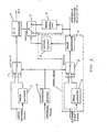
- the reference subcarrier to demodulate the R-Y signal whose phase, if the average phase of alternating burst signal is 180°, is 90°, is applied to one input terminal A of a second switching circuit. And at the same time the reference subcarrier is inverted at a phase inverter 7, and the inverted reference subcarrier whose phase is -90° is applied to another input terminal B of the second switching circuit.
- This second switching circuit 5 is controlled by the switching signal from a control circuit 6 so that the phase of the output of the second switching circuit 5 is either +90° or -90; and the output of the second switching circuit 5 is applied to the R-Y demodulator 3.
- the phase of the alternating burst signal applied to the input terminal A of the third switching circuit 9 is alternately +135° and -135°, and the phase of the burst signal through a phase inverter 8 to the input terminal B is alternately -45° and +45°, and f H/ 2 switching pulse is applied to the switch control terminal of the third switching circuit.
- the burst detecting output of a phase discrimination circuit 10 which performs homodyne detecting of the burst signal using the reference subcarrier whose phase is +90° takes on a positive polarity in state (a), and takes on a negative polarity in state (b).
- a control circuit 6 controls the connection of the switching circuit 5 so that the output of R-Y demodulator 3 can obtain an R-Y color difference signal having correct polarity under both states (a) and (b).
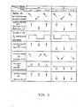
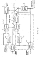
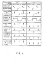
- Fig. 3 shows another embodiment of this invention and Fig. 4 shows a vector and wave diagram of the embodiment.
- this embodiment obtains different burst detecting outputs in polarity.
- the alternating burst signal is detected synchronously at the phase discriminator 10 using the reference subcarrier whose phase is +90° , and the burst detecting output signal is directly fed to the input terminal A of a fourth switching circuit 11 and a signal with the polarity inverted the output signal is fed to another input terminal B.
- f H/ 2 switching pulse is supplied to the switch control terminal of the fourth switching circuit.
- this invention allows the realization of a new demodulator circuit for color television signals of PAL system, in which the correct polarity (R-Y) signal can be obtained with just the generation of the f H /2 line switching signal, for which phase control is not exercised.
Landscapes
- Engineering & Computer Science (AREA)
- Multimedia (AREA)
- Signal Processing (AREA)
- Processing Of Color Television Signals (AREA)
- Color Television Systems (AREA)
Applications Claiming Priority (2)
| Application Number | Priority Date | Filing Date | Title |
|---|---|---|---|
| JP105464/80 | 1980-07-30 | ||
| JP10546480A JPS5730486A (en) | 1980-07-30 | 1980-07-30 | Chrominance demodulator |
Publications (3)
| Publication Number | Publication Date |
|---|---|
| EP0045221A2 true EP0045221A2 (de) | 1982-02-03 |
| EP0045221A3 EP0045221A3 (en) | 1982-02-17 |
| EP0045221B1 EP0045221B1 (de) | 1984-12-05 |
Family
ID=14408293
Family Applications (1)
| Application Number | Title | Priority Date | Filing Date |
|---|---|---|---|
| EP81303496A Expired EP0045221B1 (de) | 1980-07-30 | 1981-07-30 | Schaltung für die Demodulation von PAL-Farbfernsehsignalen |
Country Status (5)
| Country | Link |
|---|---|
| US (1) | US4417271A (de) |
| EP (1) | EP0045221B1 (de) |
| JP (1) | JPS5730486A (de) |
| AU (1) | AU527475B2 (de) |
| DE (1) | DE3167606D1 (de) |
Cited By (2)
| Publication number | Priority date | Publication date | Assignee | Title |
|---|---|---|---|---|
| EP0206199A3 (en) * | 1985-06-17 | 1989-03-08 | Pioneer Electronic Corporation | Color burst phase detection system for use in a video disk player system |
| GB2429356A (en) * | 2005-08-17 | 2007-02-21 | Snell & Wilcox Ltd | Colour error correction after composite colour coding demodulation |
Family Cites Families (6)
| Publication number | Priority date | Publication date | Assignee | Title |
|---|---|---|---|---|
| NZ153182A (de) * | 1967-07-19 | |||
| JPS502330B1 (de) * | 1970-11-17 | 1975-01-25 | ||
| SE385075B (sv) * | 1971-06-25 | 1976-05-31 | Matsushita Electric Industrial Co Ltd | Fergtelevisionsmottagare |
| GB1448979A (en) * | 1973-01-04 | 1976-09-08 | Emi Ltd | Circuit arrangements for colour television receivers |
| US4337477A (en) * | 1979-04-19 | 1982-06-29 | Matsushita Electric Industrial Co., Ltd. | Color demodulating apparatus |
| US4300155A (en) * | 1979-04-19 | 1981-11-10 | Matsushita Electric Industrial Co., Ltd. | PAL Demodulator having non-synchronized line switch |
-
1980
- 1980-07-30 JP JP10546480A patent/JPS5730486A/ja active Pending
-
1981
- 1981-07-27 US US06/286,756 patent/US4417271A/en not_active Expired - Lifetime
- 1981-07-30 EP EP81303496A patent/EP0045221B1/de not_active Expired
- 1981-07-30 AU AU73588/81A patent/AU527475B2/en not_active Ceased
- 1981-07-30 DE DE8181303496T patent/DE3167606D1/de not_active Expired
Cited By (2)
| Publication number | Priority date | Publication date | Assignee | Title |
|---|---|---|---|---|
| EP0206199A3 (en) * | 1985-06-17 | 1989-03-08 | Pioneer Electronic Corporation | Color burst phase detection system for use in a video disk player system |
| GB2429356A (en) * | 2005-08-17 | 2007-02-21 | Snell & Wilcox Ltd | Colour error correction after composite colour coding demodulation |
Also Published As
| Publication number | Publication date |
|---|---|
| EP0045221A3 (en) | 1982-02-17 |
| DE3167606D1 (en) | 1985-01-17 |
| AU7358881A (en) | 1982-02-04 |
| JPS5730486A (en) | 1982-02-18 |
| EP0045221B1 (de) | 1984-12-05 |
| AU527475B2 (en) | 1983-03-03 |
| US4417271A (en) | 1983-11-22 |
Similar Documents
| Publication | Publication Date | Title |
|---|---|---|
| US4072984A (en) | Chrominance-luminance separator | |
| US3267211A (en) | Colour television receivers | |
| EP0045221A2 (de) | Schaltung für die Demodulation von PAL-Farbfernsehsignalen | |
| US4337477A (en) | Color demodulating apparatus | |
| EP0003169B1 (de) | SECAM-PAL Fernsehsignal Transcoder und mit diesem Transcoder ausgestatteter Empfänger | |
| US4300155A (en) | PAL Demodulator having non-synchronized line switch | |
| US5192997A (en) | Automatic method for identifying a color tv standard | |
| US5301015A (en) | NTSC and PAL compatible digital encoder | |
| US4296433A (en) | Color television receiving system with forced chroma transients | |
| EP0364967B1 (de) | Luminanz-/Chrominanzsignaltrennschaltung für PAL-Farbfernsehsignale | |
| US3721753A (en) | Color television receiver | |
| KR100248789B1 (ko) | 전송표준의 디지털식 별용회로장치 | |
| GB2102237A (en) | Chrominance signal processing circuits | |
| GB1239052A (de) | ||
| US4151551A (en) | Programmable color enable and sequencing system for secam | |
| JP3080707B2 (ja) | テレビジョン方式判別回路 | |
| KR950010392Y1 (ko) | 방송방식의 혼용사용이 가능한 피아이피 시스템 | |
| KR940000157B1 (ko) | 칼라 tv의 3시스템 자동 전환장치 및 방법 | |
| SU711703A1 (ru) | Декодирующее устройство телевизионного приемника системы "секам" | |
| JPS58141092A (ja) | カラ−テレビ受像機における方式自動切換回路 | |
| JPS6321397B2 (de) | ||
| US5235411A (en) | Signal processing apparatus with improved alignment switching between color difference signals | |
| JP2508425B2 (ja) | テレビジヨン受信機 | |
| JPS56141685A (en) | Color demodulation equipment | |
| JPH033991B2 (de) |
Legal Events
| Date | Code | Title | Description |
|---|---|---|---|
| PUAI | Public reference made under article 153(3) epc to a published international application that has entered the european phase |
Free format text: ORIGINAL CODE: 0009012 |
|
| PUAL | Search report despatched |
Free format text: ORIGINAL CODE: 0009013 |
|
| AK | Designated contracting states |
Designated state(s): DE GB NL |
|
| AK | Designated contracting states |
Designated state(s): DE GB NL |
|
| 17P | Request for examination filed |
Effective date: 19820805 |
|
| GRAA | (expected) grant |
Free format text: ORIGINAL CODE: 0009210 |
|
| AK | Designated contracting states |
Designated state(s): DE GB NL |
|
| REF | Corresponds to: |
Ref document number: 3167606 Country of ref document: DE Date of ref document: 19850117 |
|
| PLBE | No opposition filed within time limit |
Free format text: ORIGINAL CODE: 0009261 |
|
| STAA | Information on the status of an ep patent application or granted ep patent |
Free format text: STATUS: NO OPPOSITION FILED WITHIN TIME LIMIT |
|
| 26N | No opposition filed | ||
| PGFP | Annual fee paid to national office [announced via postgrant information from national office to epo] |
Ref country code: GB Payment date: 19950719 Year of fee payment: 15 |
|
| PGFP | Annual fee paid to national office [announced via postgrant information from national office to epo] |
Ref country code: DE Payment date: 19950725 Year of fee payment: 15 |
|
| PGFP | Annual fee paid to national office [announced via postgrant information from national office to epo] |
Ref country code: NL Payment date: 19950727 Year of fee payment: 15 |
|
| PG25 | Lapsed in a contracting state [announced via postgrant information from national office to epo] |
Ref country code: GB Effective date: 19960730 |
|
| PG25 | Lapsed in a contracting state [announced via postgrant information from national office to epo] |
Ref country code: NL Effective date: 19970201 |
|
| GBPC | Gb: european patent ceased through non-payment of renewal fee |
Effective date: 19960730 |
|
| NLV4 | Nl: lapsed or anulled due to non-payment of the annual fee |
Effective date: 19970201 |
|
| PG25 | Lapsed in a contracting state [announced via postgrant information from national office to epo] |
Ref country code: DE Effective date: 19970402 |