EP0043844B1 - Dc to dc voltage conversion apparatus - Google Patents
Dc to dc voltage conversion apparatus Download PDFInfo
- Publication number
- EP0043844B1 EP0043844B1 EP81900469A EP81900469A EP0043844B1 EP 0043844 B1 EP0043844 B1 EP 0043844B1 EP 81900469 A EP81900469 A EP 81900469A EP 81900469 A EP81900469 A EP 81900469A EP 0043844 B1 EP0043844 B1 EP 0043844B1
- Authority
- EP
- European Patent Office
- Prior art keywords
- power
- conversion units
- terminals
- voltage
- circuit
- Prior art date
- Legal status (The legal status is an assumption and is not a legal conclusion. Google has not performed a legal analysis and makes no representation as to the accuracy of the status listed.)
- Expired
Links
- 238000006243 chemical reaction Methods 0.000 title claims description 42
- 239000003990 capacitor Substances 0.000 claims description 46
- 238000004804 winding Methods 0.000 claims description 32
- 230000000737 periodic effect Effects 0.000 claims description 5
- 238000001914 filtration Methods 0.000 claims 2
- 238000010586 diagram Methods 0.000 description 6
- 230000033228 biological regulation Effects 0.000 description 3
- 238000001514 detection method Methods 0.000 description 2
- 230000004907 flux Effects 0.000 description 2
- 238000012544 monitoring process Methods 0.000 description 2
- 229910000976 Electrical steel Inorganic materials 0.000 description 1
- XUIMIQQOPSSXEZ-UHFFFAOYSA-N Silicon Chemical compound [Si] XUIMIQQOPSSXEZ-UHFFFAOYSA-N 0.000 description 1
- 239000000654 additive Substances 0.000 description 1
- 230000000996 additive effect Effects 0.000 description 1
- 230000001276 controlling effect Effects 0.000 description 1
- 230000000694 effects Effects 0.000 description 1
- 238000010438 heat treatment Methods 0.000 description 1
- 230000010354 integration Effects 0.000 description 1
- 238000012806 monitoring device Methods 0.000 description 1
- 230000001105 regulatory effect Effects 0.000 description 1
- 238000007493 shaping process Methods 0.000 description 1
- 229910052710 silicon Inorganic materials 0.000 description 1
- 239000010703 silicon Substances 0.000 description 1
- 230000001629 suppression Effects 0.000 description 1
- 230000001960 triggered effect Effects 0.000 description 1
Images


Classifications
-
- H—ELECTRICITY
- H02—GENERATION; CONVERSION OR DISTRIBUTION OF ELECTRIC POWER
- H02J—CIRCUIT ARRANGEMENTS OR SYSTEMS FOR SUPPLYING OR DISTRIBUTING ELECTRIC POWER; SYSTEMS FOR STORING ELECTRIC ENERGY
- H02J1/00—Circuit arrangements for DC mains or DC distribution networks
- H02J1/10—Parallel operation of DC sources
- H02J1/102—Parallel operation of DC sources being switching converters
-
- H—ELECTRICITY
- H02—GENERATION; CONVERSION OR DISTRIBUTION OF ELECTRIC POWER
- H02M—APPARATUS FOR CONVERSION BETWEEN AC AND AC, BETWEEN AC AND DC, OR BETWEEN DC AND DC, AND FOR USE WITH MAINS OR SIMILAR POWER SUPPLY SYSTEMS; CONVERSION OF DC OR AC INPUT POWER INTO SURGE OUTPUT POWER; CONTROL OR REGULATION THEREOF
- H02M3/00—Conversion of DC power input into DC power output
- H02M3/22—Conversion of DC power input into DC power output with intermediate conversion into AC
- H02M3/24—Conversion of DC power input into DC power output with intermediate conversion into AC by static converters
- H02M3/28—Conversion of DC power input into DC power output with intermediate conversion into AC by static converters using discharge tubes with control electrode or semiconductor devices with control electrode to produce the intermediate AC
- H02M3/325—Conversion of DC power input into DC power output with intermediate conversion into AC by static converters using discharge tubes with control electrode or semiconductor devices with control electrode to produce the intermediate AC using devices of a triode or a transistor type requiring continuous application of a control signal
- H02M3/335—Conversion of DC power input into DC power output with intermediate conversion into AC by static converters using discharge tubes with control electrode or semiconductor devices with control electrode to produce the intermediate AC using devices of a triode or a transistor type requiring continuous application of a control signal using semiconductor devices only
- H02M3/33569—Conversion of DC power input into DC power output with intermediate conversion into AC by static converters using discharge tubes with control electrode or semiconductor devices with control electrode to produce the intermediate AC using devices of a triode or a transistor type requiring continuous application of a control signal using semiconductor devices only having several active switching elements
Definitions
- the present invention relates to voltage converters and, more particularly, to DC-to-DC voltage converters wherein a plurality of converters are serially connected across a relatively high voltage source to produce a relatively low voltage, high current output.
- the available source voltage is often too high a magnitude to permit utilization of a single solid-state converter.
- electric transit vehicles normally operate from a 600 volt direct current (DC) source since that voltage is necessary for the DC motors which propel the vehicle.
- DC direct current
- the controls, the lighting and the heating systems on such vehicles typically require a lower voltage in the range of 37.5 volts DC.
- conversion of the 600 volts to 37.5 volts can be accommodated by motor/generator sets or by silicon controlled rectifiers and silicon steel laminated transformers, such units have historically been both large, heavy and inefficient.
- the solid-state converters are necessarily switching converters and in the case of serially connected converters include transformers which enable their multiple output currents to be summed.
- a single switching device cyclically connects a transformer primary winding across a power source so that power is inductively coupled to the converter output via the transformer secondary winding. Since it is desired to actually produce a DC output voltage from the converter with minimum ripple content, the transformer and switching device must be capable of operating at relatively high frequency. However, the converter cost escalates appreciably with any increase in the required capability of the components to operate at higher frequencies.
- full wave converters are commonly employed.
- the full wave converter circuits have potential overlap problems, i.e., simultaneous conduction of switching devices such as transistors at the end of each cycle or simply due to noise may cause high thermal dissipation or failure of a transistor.
- An alternative to the full wave converter is disclosed in U.S. patent specification No. 4,195,333, published on 25 March 1980, inventor K. K. Hedel. Hedel describes a staggered mode DC to DC converter which utilizes a pair of half-wave transformer coupled stages which attain the power handling advantages of the full wave converter without the potential overlap problem.
- the Hedel converter significantly reduces the input and output filter requirements, has the ability to run at greater than 50 per cent duty factor to hold regulation under low source voltage conditions and incorporates a series connection of the transformer reset windings permitting operation of one of the half-wave sections to aid in the resetting of the transformer in the other half-wave section.
- the present invention as claimed in Claim 1 overcomes the problem of undesirable current imbalance and ripple in the DC output voltage of series connected stagger-mode converters by separating the two stages of each converter and arranging the stages into two parallel regulated power phases.
- the staggered-mode converter contains two stages, one of which is conductive during a first half-cycle (a phase one stage) and the other of which is conductive during a second half-cycle (a phase two stage).
- the phase of one stage of each converter is separated from the phase two stage and all the phase one stages are connected in one series string while the phase two stages are connected in a second series string.
- the phase one stage is shunted by one capacitor and the phase two stage is shunted by a second capacitor.
- balancing of the current between the phase one and phase two stages is accomplished by varying the conduction time of the phase one stages through a closed loop balance circuit.
- a current control loop varies the conduction of both the phase one and phase two stages in order to regulate the power output of the system.
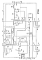
- the power circuit 10 is comprised of two single ended conversion units identified at 12 and 14.
- the unit 12 will be referred to as the phase one (01) unit and the unit 14 will be referred to as the phase two (02) unit.
- the power circuit 10 is substantially identical to that circuit shown in the aforementioned Hedel patent specification. A major distinction between the Hedel power circuit and that shown here is that the power input terminals for the two conversion units 12 and 14 have been separated.
- the 01 conversion unit 12 is provided with first and second power input terminals 16 and 18. Connected between the input terminals 16 and 18 are a primary winding 20 of a single ended power transformer 22 and a power transistor 24. Transistor 24 has alternative conductive and non conducting states, and function as a switching means to permit the power applied across terminals 16 and 18 to be applied to the transformer winding 20.
- a surge suppression or snubber circuit comprising a diode 26, capacitor 28 and resistor 30 is connected across the primary winding 20.
- a load line shaping circuit 31 is connected across the collector-emitter junction of transistor 24.
- Output power from the conversion unit 12 is developed across secondary winding 32 of transformer 22.
- One end of secondary winding 32 is connected via a rectifying diode 34 and filter reactor 36 to a first output terminal 38 of the power circuit 10.
- a second end of winding 32 is connected directly to a second output terminal 40 of circuit 10.
- a load free wheeling diode 42 is connected in parallel with the series combination of winding 32 and rectifying diode 34 to provide a path for the load current during reset of transformer 22.
- a snubber circuit comprising a resistor 46 and a capacitor 44 is connected in parallel with diode 42.
- a snubber circuit comprising a resistor 43 and a capacitor 45 is also connected in parallel with diode 34.
- Control of transistor 24 is affected by signals applied to control signal input terminals (or simply control terminals) 45 and 50; in operation, as will be seen hereinafter, these control terminals 48 and 50 receive control signals, more specifically periodic energizing or gating signals 01 (produced by unit 128, Fig. 3A) effective to energize or activate the conversion unit 12.
- the terminals 48 and 50 are connected, respectively to first and second terminals of a primary winding 52 of a signal transformer 54.
- a secondary winding 56 of transformer 54 has one terminal connected to an emitter terminal of transistor 24 and a second terminal connected through a resistor 58 to a base terminal of transistor 24.
- a capacitor 60 is connected in parallel with resistor 58 so that the combination of capacitor 60 and resistor 58 acts as a differentiating filter for gating signals applied to the input terminals 48 and 50 to speed up the switching of the transistor 24 between its mentioned conducting and non-conducting states.
- the transistor 24 In operation the transistor 24 is in its conducting state during intermittent intervals determined by the pulse width of the gating signals 01; it will change states at a frequency corresponding to the gating frequency.
- the DC to DC converter 10 is arranged so that current always flows from the terminal 16 to the terminal 18 through the transformer primary winding 20, it is necessary to reset the transformer flux level after each current pulse in order to avoid saturation. Accordingly, there is provided a reset winding 62 within the transformer 22.
- the reset winding is connected across the output terminals 38 and 40 of the power circuit 10 whereby, because winding 62 is reverse wound with respect to the other windings of transformer 22, the output voltage forces a current through winding 62 which drives the transformer flux in a direction to avoid saturation.
- Current through the winding 62 is limited by series connected resistor 64 and inductor 66 in the winding 62 current path.
- an alternative arrangement is to provide a separate power supply for exciting the reset winding 62. Where several power circuits are used, the reset windings may be serially connected.
- the 02 conversion unit 14 is identical to the 01 unit 12 and is provided with power input terminals 68 and 70 between which are connected a transistor 72 and a primary winding 74 of a transformer 76.
- a secondary winding 77 of transformer 76 has one terminal connected to power output terminal 40 and a second terminal connected through a diode 78 and filter reactor 80 to power output terminal 38.
- the power output terminals 38, 40 are shared by the otherwise separate conversion units 12, 14.
- Energizing or gating signals 02 (produced by unit 130, Fig. 3A) fortransistor72 are periodically applied to control terminals 82 and 84 from which terminals they are coupled through a signal transformer 86 and applied across the base-emitter junction of transistor 72.
- Power transformer 76 is also provided with a reset winding 88 which is serially connected in a current path with reset winding 62.
- the gating signals 02 are staggered with respect to the gating signals 01, and hence the time intervals of conduction of transistor 72, and of transistor 24 are staggered with respect to each other.
- a power balancing arrangement is necessary in order to insure that the average currents supplied by each of the conversion units 12 and 14 are equal so that transistor currents are equalized and ripple currents are minimized.
- appropriate currents measuring devices are provided for each unit 12 and 14.
- these measuring devices are indicated as current sensing coils 90 and 92 connected, respectively, in the emitter circuits of transistors 24 and 72.
- the coil 90 provides an output current signal indicated as 101 at terminals 94 and 96.
- the coil 92 provides an output current signal indicated as 1 02 at terminals 98 and 100.
- the signals 1 01 and 1 02 are representative of the current flowing through the transistors 24 and 72 during their respective conduction intervals.
- one of the advantages of the present invention is the avoidance of the necessity of supplying current sensing coils in each conversion unit when the power circuits are connected in a series arrangement.
- the power circuit 10 is explained and its operation detailed in the aforementioned Hedel patent specification. In essence a signal is applied to terminals 48 and 50 to gate transistor 24 into conduction for a predetermined portion of a first "half-cycle". Thereafter, a signal is applied to terminals 82 and 84 to gate transistor 72 into conduction for a second "half-cycle". The transistors 24 and 72 are therefore alternately gated into conduction to provide interdigitated pulses of current to the output terminals 38 and 40 of the power circuit 10 as indicated herein above.
- the rectifying diodes 34 and 78 assure that the current to terminals 38 and 40 is unidirectional and the voltage developed is of the desired polarity.
- the filter reactors 36 and 80 in conjunction with a filter capacitor 102 serves to smooth the output current so that it is relatively ripple free. The magnitude of the output voltage is controlled by adjusting the conduction time intervals or duty cycles of the transistors 24 and 72.
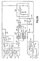
- FIG. 2 there is shown a block diagram of a preferred embodiment of the present invention.
- The-blocks labeled 10A, 10B, 10C and 10D each represent a converter power circuit or "conversion unit" substantially identical to the circuit 10 illustrated in Fig. 1.
- Each of the converter power circuits includes respective power output terminals 38A, B, C or D and 40A, B, C or D.
- the Terminals 38A, 38B, 38C and 38D are all connected to a shared or common terminal 104 and the terminals 40A, 40B, 40C and 40D are connected to a shared or common terminal 106.
- the currents from each of the power circuits 10A, 10B, 10C and 10D are additive and the capacitor 102 is connected between the common terminals 104 and 106.
- the control signal input terminals of the converter power circuit 10A are designated 48A, 50A, 82A and 84A, and similarly (but with suffix letters B; C D) for the control terminals of the remaining units 10B, 10C, 10D.
- All the terminals 48 and 50 are connected so that a common gating signal 01 is simultaneously applied to all the phase one conversion units 12A, 12B, 12C and 12D.
- all the terminals 82 and 84 are connected so that a common gating signal 02 is simultaneously applied to all the phase two conversion units 14A, 14B, 14C and 14D.
- the converter power circuits 10A, 10B, 10C and 10D are each provided with power input terminals corresponding to the terminals 16, 18, 68 and 70 of the power circuit illustrated in Fig. 1.
- the power input terminals are accordingly numbered as in Fig. 1 but with suffixes A, B, C or D indicating, respectively, their association with power circuits 10A, 10B, 10C or 10D.
- the terminals 16A and 68A of power circuit 10A are connected to a relatively positive potential input power bus 108.
- the terminals 18A and 70A of power circuit 10A are connected, respectively, to input terminals 16B and 68B of power circuit 10B.
- a plurality of power circuits such as power circuit 10 can be serially connected across a power source such that each power circuit is subjected to only a proportionate fraction of the source potential.
- four such power circuits are shown although the number can be reduced or increased as desired to meet power output or voltage input requirements.
- the final power circuit i.e., 1 OD in the embodiment of Fig. 2 has its input terminals 16D and 68D connected, respectively, to the terminals 18C and 70C of the immediately preceding power circuit 10C.
- the terminals 18D and 70D of power circuit 10D are connected to the relatively negative potential input power bus 110.
- the power input bus 108 is connected to a relatively positive potential terminal of a DC power source (not shown) through a line inductor 112, a noise filter 114, a line breaker 116 and a current limit fuse 118.
- the bus 110 is connected to a relatively negative potential terminal of the DC power source.
- the voltage developed between buses 108 and 110 is divided into a number of equipotential parts by a capacitive voltage divider comprising eight equal value capacitors arranged as a first series connected string of capacitors 120, 121, 122, and 123 and a second series connected string of capacitors 124, 125, 126 and 127, each of the series strings of capacitors being connected between the buses 108 and 110.
- the first series string of capacitors is associated with the phase one (01) conversion units of the power circuits 10A, 10B, 10C and 10D. More specifically, the capacitor 120 is connected between the input terminals 16A and 18A of power circuit 10A, the capacitor 121 is connected between the input terminals 16B and 18B of power circuit 10B, the capacitor 122 is connected between the input terminals 16C and 18C of power circuit 10C, and the capacitor 123 is connected between the input terminals 16D and 18D of power circuit 10D.
- the capacitor 124 is connected between the input terminals 68A and 70A of power circuit 10A, the capacitor 125 is connected between the input terminals 68B and 70B of power circuit 10B.
- the capacitor 126 is connected between the input terminals 68C and 70C of power circuit 10C, and the capacitor 127 is connected between the input terminals 68D and 70D of power circuit 10D.
- the 01 conversion units are associated with the first series connected string of capacitors 120, 121, 122 and 123 whereas the 02 conversion units are associated with the second series connected string of capacitors 124, 125, 126 and 127.
- the prior art has suggested that only a single capacitive voltage divider string need be used.
- U.S. Patent 4,062,057 such an arrangement is shown in U.S. Patent 4,062,057.
- use of a single capacitive voltage divider network requires very expensive and careful matching of the components in all the power circuits in order to balance transistor currents between the 01 and 02 units.
- the balance cannot be maintained over the normal temperature range of operation. Balancing of the currents is possible if current transformers are provided for each of the individual conversion units and if individual balance control circuits are provided for each power circuit.
- each capacitor in our arrangement is subject to the same voltage rating but need only be one-half of the former microfarad capacitance rating.
- the 01 transistors for each power circuit are in series and the 02 transistors for each power circuit are in series so that only a single balancing circuit is required to force the average current in each conversion unit to balance.
- the power circuit 10D is shown as including current monitor devices for providing current signals 10i and 1 02 at output terminal pairs 94, 96 and 98, 100, respectively.
- Fig. 2 also illustrates the use of two power supplies 129 and 131 which are adapted to provide the low voltage power for the power control circuit 133 which regulates the output voltage developed across capacitor 102. Because of the relatively high voltage developed between buses 108 and 110, two power supplies working against the center tap between capacitors 121 and 122 are used rather than only one supply.
- the block 135 represents the series connection of all the reset windings of the power circuits 10A, 10B, 10C and 10D. As mentioned previously, where a plurality of conversion units are employed, a separate power supply may be provided for the reset windings rather than tap the reset current from the available output power at capacitor 102.
- Figs. 3A and 3B there is shown a more detailed schematic and block diagram of the power control circuit 133.
- the gating signals 01, 02 are supplied to each of the power circuits 10A, 10B, 10C and 10D from transistor gate driver circuits 128 and 130 of a type well known in the art.
- the gating signals are initiated by a circuit including a two-phase oscillator 132 which generates two square-wave signals that are 180° out of phase from one another.
- the square-wave signals are each converted to triangular wave-forms by integration networks comprising, respectively, a resistor 134 and capacitor 136 and a resistor 138 and capacitor 140.
- the triangular waveforms are applied to respective comparators 142 and 144 where they are compared with signals representing any difference between the measured average voltage magnitude and the desired voltage magnitude in order to generate gating signals at appropriate times for controlling the conduction time intervals or duty cycles of the power stages 10A, 10B, 10C and 10D in a manner to minimize that difference.
- balance correction circuit 146 (Fig. 3B) connected for receiving the 1 01 and 1 02 current signals produced by the current monitoring devices in power circuit 10D.
- Balance circuit 146 includes first input terminals 148 and 150 for receiving the 1 01 signal and second input terminals 152 and 154 for receiving the I m2 signal. Because the 1 01 and 1 02 signals are pulse signals, the signals are rectified and filtered before being applied to an amplifier 156. The 1 01 signal is applied across a resistor 158 connected between the first input terminals 148 and 150.
- the series combination of a rectifying diode 160 and resistor 162 is connected in parallel with resistor 158.
- the signal developed at the circuit junction point of diode 160 and resistor 162 is coupled through a resistor 164 to a non-inverting input terminal of amplifier 156.
- a filter capacitor 166 is connected between the non-inverting input terminal of amplifier 156 and the balance circuit first input terminal 150, which input terminal is also connected to signal ground.
- the 1 02 signal is applied across a resistor 168 connected between the second input terminals 152 and 154.
- the series combination of a rectifying diode 170 and resistor 172 is connected in parallel with resistor 168.
- the circuit junction point of diode 170 and resistor 172 is connected through a resistor 174 to an inverting input terminal of amplifier 156.
- Input terminal 154 is also connected to signal ground.
- the amplifier 156 is connected as an integrating amplifier and as such has a feedback capacitor 176 connected between its inverting input terminal and its output terminal.
- the signal developed at the output terminal of amplifier 156, and the circuit 146, is representative of the average difference between the 1 01 and 1 02 signals.
- This difference signal is coupled through a resistor 178 to a junction 180 at the inverting input terminal of amplifier 142 (Fig. 3A).
- the difference signal acts as an offset to the triangular waveform developed at junction 180 and thus varies the pulse width of the gate signal applied to the 01 conversion units in a manner to minimize the difference signal.
- Regulation of the output voltage produced by the power circuits 10 is accomplished by a feedback circuit of a type well known in the art.
- the output voltage is monitored and a signal Vo representative thereof is coupled to an input terminal 182 of an amplifier circuit 184.
- a second input terminal 186 of circuit 184 is connected to receive a reference signal V ref representative of a desired magnitude of output voltage.
- the circuit 184 may be a common type of operational amplifier arrangement including a high gain amplifier 188, a feedback impedance 190 connected between the inverting input terminal and an output terminal of amplifier 188 and an input impedance 192 connected between input terminal 182 and the inverting input terminal of amplifier 188.
- the input terminal 186 is connected to the non-inverting input terminal of amplifier 188.
- the output terminal of amplifier circuit 184 is connected to the non-inverting input terminals of both amplifiers 142 and 144 (Fig. 3A) through input resistors 194 and 196, respectively.
- the amplifiers 142 and 144 compare the voltage error signal produced by amplifier circuit 184 to the triangular waveform and produce gate drive signals at the appropriate crossover points.
- the 1 0 , and 1 02 signals are also utilised as input signals to a current limit circuit which monitors both peak current and average current.
- the rectified current signal developed at the junction of diode 160 and resistor 164 (Fig. 3B) is applied to a first input terminal of a summing junction 198.
- a second input terminal of junction 198 is connected to the junction of diode 170 and resistor 174.
- the output signal developed by summing junction 198 thus represents the total current supplied by all the power circuits 10A, 10B, 10C and 10D.
- An output terminal of junction 198 is connected to input terminals of both a peak current limit circuit 200 and an average current limit 202.
- Both limit circuits 200 and 202 are essentially level detectors of a type well known in the art.
- the peak limit circuit 200 is preferably biased to respond to a current surge of short duration which exceeds the average current limit level by about twenty per cent.
- the output signals developed by both circuits 200 and 202 are coupled to a common junction 204 via a diode or circuit comprising the diodes 206 and 208.
- the junction 204 is connected to an inverting input terminal of an amplifier 210.
- An integrator comprising a resistor 212 and capacitor 214 is connected between junction 204 and signal ground.
- the integrator eliminates false detections and also serves to hold the system off for a reasonable time when a true current is observed.
- the amplifier 210 is connected as a comparator and as such has a bias applied to its non-inverting input terminal by means of a voltage divider comprising the resistors 216 and 218 which are serially connected between a voltage source +V and signal ground with the junction mediate the resistors connected to the non-inverting input terminal. Furthermore, when triggered, amplifier 210 is held in a latched state until the trigger signal drops below a pre-determined level. This latter function is achieved by a Zener diode 220 connected between the non-inverting input terminal and an output terminal of amplifier 194.
- amplifier 210 Signals developed at the output terminal of amplifier 210 are coupled through a resistor 222 and a diode 224 to the output terminal of circuit 184. Since amplifier 210 in the illustrated embodiment acts as a comparator to switch its output state to a relatively negative voltage on an overcurrent condition, the effect of an overcurrent detection is to pull the error signal applied to amplifiers 142 and 144 to a negative level whereby no gating signals can be generated.
- a "slew-on" circuit 226 (Fig. 3A) whose output is also connected to the junction of resistors 194 and-196.
- One of the input signals to the circuit 226 is the overcurrent signal from amplifier 210 (Fig. 3B) which is connected to the circuit 226 through a comparator 228 and an inverter 230.
- the overcurrent signal is applied to a junction 232 at the non-inverting input terminal of an amplifier 234.
- An integrator comprising resistor 236 and capacitor 238 is discharged by the signal from comparator 228 and the capacitor charge time established by the integrator sets the slew rate for returning the gate signals to their desired level. Since the circuit 226 is well known in the art, no further description of its components is deemed necessary.
- the present system also incorporates voltage monitoring to assure that the available line voltage is within the desired operating range of the power circuits 10 and that the voltage generated by the system's DC power supplies are within a desired range.
- voltage monitoring to assure that the available line voltage is within the desired operating range of the power circuits 10 and that the voltage generated by the system's DC power supplies are within a desired range.
- Such monitoring arrangements are commonly known and utilized and therefore no details of such arrangements are included herein.
- a signal V L representative of line voltage magnitude is applied to a comparator 240 through a diode OR circuit 242 (Fig. 3A).
- a signal Vp s representative of power supply voltage magnitude is also applied through OR circuit 242 to comparator 240. If the signals V L or Vp s indicate either an overvoltage or undervoltage condition, the comparator 240 provides a signal to junction 232 in circuit 226 to force the termination of gate signals supplied by amplifiers 142 and 144.
- a distinct advantage of the present invention is the modularity concept which it offers.
- the control function is essentially independent of the number of power converters in the system.
- the power control unit depends only on the monitored system output voltage and currents flowing in the final stagger-mode converter in the series string of converters. Accordingly, converters can be added to or deleted from the string as desired to vary the power handling capability of the system without changing the control system.
Landscapes
- Engineering & Computer Science (AREA)
- Power Engineering (AREA)
- Dc-Dc Converters (AREA)
Applications Claiming Priority (2)
| Application Number | Priority Date | Filing Date | Title |
|---|---|---|---|
| US111616 | 1980-01-14 | ||
| US06/111,616 US4313155A (en) | 1980-01-14 | 1980-01-14 | High input voltage DC to DC power converter |
Publications (3)
| Publication Number | Publication Date |
|---|---|
| EP0043844A1 EP0043844A1 (en) | 1982-01-20 |
| EP0043844A4 EP0043844A4 (en) | 1983-04-06 |
| EP0043844B1 true EP0043844B1 (en) | 1985-05-15 |
Family
ID=22339491
Family Applications (1)
| Application Number | Title | Priority Date | Filing Date |
|---|---|---|---|
| EP81900469A Expired EP0043844B1 (en) | 1980-01-14 | 1981-01-05 | Dc to dc voltage conversion apparatus |
Country Status (8)
| Country | Link |
|---|---|
| US (1) | US4313155A (enExample) |
| EP (1) | EP0043844B1 (enExample) |
| JP (1) | JPS56501906A (enExample) |
| BR (1) | BR8105863A (enExample) |
| ES (1) | ES8201370A1 (enExample) |
| IT (1) | IT1135023B (enExample) |
| MX (1) | MX148862A (enExample) |
| WO (1) | WO1981002077A1 (enExample) |
Cited By (1)
| Publication number | Priority date | Publication date | Assignee | Title |
|---|---|---|---|---|
| DE3705392A1 (de) * | 1987-02-20 | 1988-09-01 | Thomson Brandt Gmbh | Schaltnetzteil |
Families Citing this family (21)
| Publication number | Priority date | Publication date | Assignee | Title |
|---|---|---|---|---|
| DE3009359A1 (de) * | 1980-03-12 | 1981-09-17 | Deutsche Automobilgesellschaft Mbh, 3000 Hannover | Ladegeraet |
| US4405893A (en) * | 1981-07-06 | 1983-09-20 | Gulton Industries, Inc. | Pulse width regulator |
| US4447741A (en) * | 1982-09-27 | 1984-05-08 | Northern Telecom Limited | Base drive circuit for power transistors |
| US4688160A (en) * | 1985-12-19 | 1987-08-18 | American Telephone And Telegraph Co., At&T Bell Labs | Single ended forward converter with resonant commutation of magnetizing current |
| JPH0626473B2 (ja) * | 1988-02-27 | 1994-04-06 | 富士通電装株式会社 | 電流バランス型スイッチングレギュレータ |
| US4890210A (en) * | 1988-11-15 | 1989-12-26 | Gilbarco, Inc. | Power supply having combined forward converter and flyback action for high efficiency conversion from low to high voltage |
| US5197228A (en) * | 1989-06-19 | 1993-03-30 | Constant Velocity Systems, Inc. | Method of and machine for grinding a workpiece |
| US5338994A (en) * | 1989-07-20 | 1994-08-16 | General Electric Company | Method and apparatus for achieving current balance in parallel connected switching devices |
| US6122186A (en) * | 1996-05-03 | 2000-09-19 | Zecal Corp. | High power miniature demand power supply |
| WO1997009772A1 (en) * | 1995-09-01 | 1997-03-13 | Philips Electronics N.V. | Power supply apparatus with improved efficiency |
| DE19547064A1 (de) * | 1995-12-18 | 1997-09-25 | Studlar Sikora Jana | Verfahren zur Hochspannungs-Umformung durch Kaskadierung |
| US6058030A (en) * | 1997-11-20 | 2000-05-02 | Intersil Corporation | Multiple output DC-to-DC converter having enhanced noise margin and related methods |
| FI117259B (fi) * | 1999-09-22 | 2006-08-15 | Abb Oy | Välipiirikondensaattoreiden jännitteen tasaus |
| AU6113401A (en) * | 2000-05-03 | 2001-11-12 | Horton Inc | Brushless dc ring motor cooling system |
| US7023187B2 (en) * | 2001-08-16 | 2006-04-04 | Intersil Americas Inc. | Integrated circuit for generating a plurality of direct current (DC) output voltages |
| DE10140783A1 (de) * | 2001-08-21 | 2003-04-03 | Inst Solare Energieversorgungstechnik Iset | Vorrichtung zum gleichberechtigten Parallelbetrieb von ein- oder dreiphasigen Spannungsquellen |
| US6667893B2 (en) * | 2002-04-25 | 2003-12-23 | International Business Machines Corporation | Phase and frequency shifted controller for interleaved ZVS forward power converter |
| US6760236B2 (en) * | 2002-09-04 | 2004-07-06 | Chih-Hung Hsieh | Third winding reset forward converter |
| US9312705B2 (en) | 2010-12-22 | 2016-04-12 | Ge Energy Power Conversion Technology Limited | Capacitor balancing circuit and control method for an electronic device such as a multilevel power inverter |
| MX2013007361A (es) | 2010-12-22 | 2013-12-06 | Ge Energy Power Conversion Technology Ltd | Disposicion mecanica de un circuito convertidor de potencia de niveles multiples. |
| CN105429201B (zh) * | 2015-11-13 | 2018-04-06 | 宁波市江北九方和荣电气有限公司 | 基于sepic电路的电容器智能充电系统 |
Family Cites Families (11)
| Publication number | Priority date | Publication date | Assignee | Title |
|---|---|---|---|---|
| CH406410A (de) * | 1963-04-18 | 1966-01-31 | Bbc Brown Boveri & Cie | Selbstgeführter Mehrphasen-Wechselrichter |
| US3818307A (en) * | 1972-07-31 | 1974-06-18 | Bell Telephone Labor Inc | Serially-connected converters having multiple regulation modes for use in supplying serially-connected loads on long lines |
| JPS52204B2 (enExample) * | 1972-08-14 | 1977-01-06 | ||
| US3913000A (en) * | 1973-05-29 | 1975-10-14 | Hughes Aircraft Co | Two-phase solid state power converter |
| US3873903A (en) * | 1974-02-15 | 1975-03-25 | Ncr Co | Volt-second balancing means for a high frequency switching power supply |
| SU604104A1 (ru) * | 1976-05-25 | 1978-04-25 | Донецкое Отделение Института "Гипроуглеавтоматизация" | Преобразователь напр жени |
| CH592979A5 (enExample) * | 1976-06-04 | 1977-11-15 | Bbc Brown Boveri & Cie | |
| US4062057A (en) * | 1977-04-15 | 1977-12-06 | The United States Of America As Represented By The Secretary Of The Navy | Regulated power supply having a series arrangement of inverters |
| DE2722339C2 (de) * | 1977-05-17 | 1986-09-11 | Siemens AG, 1000 Berlin und 8000 München | Schaltungsanordnung zur Erzeugung von Spannungen mit wechselnder Polarität aus einer Gleichspannung |
| US4176392A (en) * | 1977-12-14 | 1979-11-27 | The United States Of America As Represented By The Secretary Of The Army | Series induction/parallel inverter power stage and power staging method for DC-DC power converter |
| US4195333A (en) * | 1978-05-30 | 1980-03-25 | General Electric Company | DC to DC voltage converter |
-
1980
- 1980-01-14 US US06/111,616 patent/US4313155A/en not_active Expired - Lifetime
-
1981
- 1981-01-05 JP JP50070081A patent/JPS56501906A/ja active Pending
- 1981-01-05 BR BR8105863A patent/BR8105863A/pt unknown
- 1981-01-05 EP EP81900469A patent/EP0043844B1/en not_active Expired
- 1981-01-05 WO PCT/US1981/000002 patent/WO1981002077A1/en not_active Ceased
- 1981-01-13 ES ES498462A patent/ES8201370A1/es not_active Expired
- 1981-01-14 IT IT19118/81A patent/IT1135023B/it active
- 1981-01-14 MX MX185554A patent/MX148862A/es unknown
Cited By (1)
| Publication number | Priority date | Publication date | Assignee | Title |
|---|---|---|---|---|
| DE3705392A1 (de) * | 1987-02-20 | 1988-09-01 | Thomson Brandt Gmbh | Schaltnetzteil |
Also Published As
| Publication number | Publication date |
|---|---|
| IT8119118A0 (it) | 1981-01-14 |
| JPS56501906A (enExample) | 1981-12-24 |
| ES498462A0 (es) | 1982-01-01 |
| MX148862A (es) | 1983-06-27 |
| WO1981002077A1 (en) | 1981-07-23 |
| IT1135023B (it) | 1986-08-20 |
| BR8105863A (pt) | 1981-11-24 |
| EP0043844A4 (en) | 1983-04-06 |
| ES8201370A1 (es) | 1982-01-01 |
| EP0043844A1 (en) | 1982-01-20 |
| US4313155A (en) | 1982-01-26 |
Similar Documents
| Publication | Publication Date | Title |
|---|---|---|
| EP0043844B1 (en) | Dc to dc voltage conversion apparatus | |
| EP0595091B1 (en) | Active three phase power conditioner | |
| US5724237A (en) | Apparatus and method for sharing a load current among frequency-controlled D.C.-to-D.C. converters | |
| US4853832A (en) | Cascaded resonant bridge converters | |
| US4827150A (en) | Uninterruptible power supply inverter circuit | |
| KR950035037A (ko) | 유도부하에 대한 제어회로 | |
| JPH03256532A (ja) | パワーコンバータ装置 | |
| US5397976A (en) | Control system for voltage controlled bilateral current source | |
| US4005352A (en) | Protection circuit for magnetically controlled d-c to d-c converter | |
| US3444457A (en) | Voltage regulator system utilizing a center-tapped inductor | |
| JPH01222659A (ja) | 電流バランス型スイッチングレギュレータ | |
| US4455598A (en) | Automatic device for compensation of AC polyphase power line voltage variations in AC-DC converters | |
| RU2020710C1 (ru) | Преобразователь частоты со звеном постоянного тока | |
| US4495555A (en) | Energy converter | |
| US4151453A (en) | Induction motor control system | |
| US4669039A (en) | Circuit arrangement for autoconverters | |
| EP0352951B1 (en) | A.C. generator fault detector | |
| JPS607908B2 (ja) | パルス幅変調を用いるマスタ−スレ−ブ電圧調整器 | |
| US4403279A (en) | Vehicular plural voltage system | |
| EP0092370A1 (en) | A.C. motor controller | |
| JPH04372525A (ja) | スイッチング電源装置 | |
| US5434769A (en) | Multi-phase adaptable AC-DC converter | |
| US4547843A (en) | Multiple output DC power supply | |
| JP2968670B2 (ja) | 保護回路付きdc−dcコンバータ | |
| SU1735978A1 (ru) | Регулируемый источник вторичного электропитани |
Legal Events
| Date | Code | Title | Description |
|---|---|---|---|
| PUAI | Public reference made under article 153(3) epc to a published international application that has entered the european phase |
Free format text: ORIGINAL CODE: 0009012 |
|
| AK | Designated contracting states |
Designated state(s): DE FR GB SE |
|
| 17P | Request for examination filed |
Effective date: 19820112 |
|
| GRAA | (expected) grant |
Free format text: ORIGINAL CODE: 0009210 |
|
| AK | Designated contracting states |
Designated state(s): DE FR GB SE |
|
| REF | Corresponds to: |
Ref document number: 3170450 Country of ref document: DE Date of ref document: 19850620 |
|
| ET | Fr: translation filed | ||
| PLBE | No opposition filed within time limit |
Free format text: ORIGINAL CODE: 0009261 |
|
| STAA | Information on the status of an ep patent application or granted ep patent |
Free format text: STATUS: NO OPPOSITION FILED WITHIN TIME LIMIT |
|
| 26N | No opposition filed | ||
| PG25 | Lapsed in a contracting state [announced via postgrant information from national office to epo] |
Ref country code: DE Effective date: 19871001 |
|
| PG25 | Lapsed in a contracting state [announced via postgrant information from national office to epo] |
Ref country code: SE Effective date: 19880106 |
|
| GBPC | Gb: european patent ceased through non-payment of renewal fee | ||
| PG25 | Lapsed in a contracting state [announced via postgrant information from national office to epo] |
Ref country code: FR Free format text: LAPSE BECAUSE OF NON-PAYMENT OF DUE FEES Effective date: 19880930 |
|
| PG25 | Lapsed in a contracting state [announced via postgrant information from national office to epo] |
Ref country code: GB Free format text: LAPSE BECAUSE OF NON-PAYMENT OF DUE FEES Effective date: 19881118 |
|
| REG | Reference to a national code |
Ref country code: FR Ref legal event code: ST |
|
| EUG | Se: european patent has lapsed |
Ref document number: 81900469.8 Effective date: 19880913 |