EP0041858B1 - Method and apparatus for deep level transient spectroscopy scanning - Google Patents
Method and apparatus for deep level transient spectroscopy scanning Download PDFInfo
- Publication number
- EP0041858B1 EP0041858B1 EP81302531A EP81302531A EP0041858B1 EP 0041858 B1 EP0041858 B1 EP 0041858B1 EP 81302531 A EP81302531 A EP 81302531A EP 81302531 A EP81302531 A EP 81302531A EP 0041858 B1 EP0041858 B1 EP 0041858B1
- Authority
- EP
- European Patent Office
- Prior art keywords
- period
- signal
- amplifier
- voltage level
- junction
- Prior art date
- Legal status (The legal status is an assumption and is not a legal conclusion. Google has not performed a legal analysis and makes no representation as to the accuracy of the status listed.)
- Expired
Links
- 238000000034 method Methods 0.000 title claims description 25
- 238000001773 deep-level transient spectroscopy Methods 0.000 title claims description 16
- 230000002441 reversible effect Effects 0.000 claims description 16
- 230000008859 change Effects 0.000 claims description 12
- 239000004065 semiconductor Substances 0.000 claims description 11
- 230000004044 response Effects 0.000 claims description 10
- 230000001052 transient effect Effects 0.000 claims description 8
- 238000004804 winding Methods 0.000 claims description 7
- 230000003111 delayed effect Effects 0.000 claims description 4
- 238000001514 detection method Methods 0.000 claims description 2
- 230000008878 coupling Effects 0.000 claims 1
- 238000010168 coupling process Methods 0.000 claims 1
- 238000005859 coupling reaction Methods 0.000 claims 1
- 238000005259 measurement Methods 0.000 description 31
- 238000010586 diagram Methods 0.000 description 13
- 230000007704 transition Effects 0.000 description 10
- 230000005540 biological transmission Effects 0.000 description 7
- 239000003990 capacitor Substances 0.000 description 6
- 230000007423 decrease Effects 0.000 description 4
- 230000005284 excitation Effects 0.000 description 4
- 230000004913 activation Effects 0.000 description 3
- 238000013461 design Methods 0.000 description 3
- 230000035945 sensitivity Effects 0.000 description 3
- 230000003247 decreasing effect Effects 0.000 description 2
- 230000001934 delay Effects 0.000 description 2
- 230000000694 effects Effects 0.000 description 2
- 230000008569 process Effects 0.000 description 2
- 238000012360 testing method Methods 0.000 description 2
- 238000012935 Averaging Methods 0.000 description 1
- 230000003321 amplification Effects 0.000 description 1
- 239000000969 carrier Substances 0.000 description 1
- 230000000295 complement effect Effects 0.000 description 1
- 230000007547 defect Effects 0.000 description 1
- 230000001419 dependent effect Effects 0.000 description 1
- 238000011161 development Methods 0.000 description 1
- 238000011156 evaluation Methods 0.000 description 1
- 238000000691 measurement method Methods 0.000 description 1
- 238000003199 nucleic acid amplification method Methods 0.000 description 1
- 230000003287 optical effect Effects 0.000 description 1
- 230000010363 phase shift Effects 0.000 description 1
- 238000003908 quality control method Methods 0.000 description 1
- 239000010453 quartz Substances 0.000 description 1
- 238000011084 recovery Methods 0.000 description 1
- 238000010079 rubber tapping Methods 0.000 description 1
- 238000005070 sampling Methods 0.000 description 1
- VYPSYNLAJGMNEJ-UHFFFAOYSA-N silicon dioxide Inorganic materials O=[Si]=O VYPSYNLAJGMNEJ-UHFFFAOYSA-N 0.000 description 1
- 238000004611 spectroscopical analysis Methods 0.000 description 1
- 230000001360 synchronised effect Effects 0.000 description 1
Images

Classifications
-
- G—PHYSICS
- G01—MEASURING; TESTING
- G01R—MEASURING ELECTRIC VARIABLES; MEASURING MAGNETIC VARIABLES
- G01R31/00—Arrangements for testing electric properties; Arrangements for locating electric faults; Arrangements for electrical testing characterised by what is being tested not provided for elsewhere
- G01R31/26—Testing of individual semiconductor devices
- G01R31/2607—Circuits therefor
- G01R31/2637—Circuits therefor for testing other individual devices
-
- G—PHYSICS
- G01—MEASURING; TESTING
- G01R—MEASURING ELECTRIC VARIABLES; MEASURING MAGNETIC VARIABLES
- G01R31/00—Arrangements for testing electric properties; Arrangements for locating electric faults; Arrangements for electrical testing characterised by what is being tested not provided for elsewhere
- G01R31/26—Testing of individual semiconductor devices
- G01R31/2607—Circuits therefor
- G01R31/2632—Circuits therefor for testing diodes
Definitions
- the invention relates to deep level transient spectroscopy (DLTS) and more particularly to a method for carrying out DLTS scanning on a semiconductor junction by measuring a predetermined sequence of the transient capacitance changes of the junction.
- the invention relates also to an apparatus for carrying out the method.
- the change of the occupancy of the localized states in the forbidden band can be measured as a change of the capacitance.
- the localized states are periodically filled and emptied, and the amplitude of the resulting periodical capacitance change is determined by the concentration of the energy states, while the kinetics thereof is determined by the activation energies and thermal capture cross-sections of the localized states as a function of temperature.
- the occupancy of the localized states are changed by voltage-, current- or light-pulses applied to the PN junction.
- This measuring method is the deep level transient spectroscopy or DLTS method as referred to hereinabove, and instruments utilising this method are indispensable factors in development and quality control work in the field of semiconductor devices.
- the measurement of the capacitance changes is carried out in such a way that the diode representing the semiconductor junction to be measured is connected into one arm of a bridge, and a compensating capacitance is inserted in the other arm of the bridge having a capacitance equal to that of the diode.
- a high frequency signal is applied to the two arms of the bridge through a symmetrical high frequency transformer.
- a train of pulses is applied to the diode through a pulse transformer.
- the repetition rate and the duty cycle of the pulsers can be adjusted within wide ranges in accordance with the DLTS method.
- a forward or slightly reverse voltage is applied to the diode, and between the ending moments of the pulses and the starting moments of the subsequent pulses a high reverse voltage is applied to the diode.
- the capacitance of the diode is substantially different under the two kinds of voltages applied thereto which difference can be as high as 2-3 decimal orders of magnitude, and during the presence of the reverse bias a capacitance transient (a decay) takes place which is typically by 4 decimal orders of magnitude smaller than the d.c. reverse capacitance.
- the task of the measurement is to determine the small capacitance changes during the reverse biasing pulses.
- the output of the measuring circuit is detected by a phase-sensitive detector following a sufficient amplification, and the so obtained pulsating voltage will be proportional to the capacitive output signal component of the measuring circuit.
- This voltage is applied to the input of a low-frequency lock-in amplifier synchronized to the starting moments of the measuring periods, and the second lock-in amplifier selects the component from the rectified pulsating input voltage which has the same frequency as the measuring periods have.
- the temperature and other parameters of the diode to be measured are changed and such changes take place much slower than the rate of pulses applied to the diode.
- the information characterizing the properties of the diode is carried by the recorded sequence of capacitance changes obtained during the pulse periods with reverse bias.
- the application of the excitation pulses is rather complicated, and in the described arrangement the stray capacitance and series inductance of the pulse transformer can result in pulse parameters other than the set values, especially if there are high conductive losses.
- the true transmission of pulses with durations that can be varied within a wide range, which wide range is required for the measurement of the capture cross-section of majority or minority carriers, can be solved precisely only by using a plurality of pulse transformers.
- the measuring amplifier receives the full driving signal, and following the significant overloading it can recover relatively slowly, i.e. the ineffective dead period of the capacitance measurement will be long, i.e. the starting section of the exponentially decaying capacitance signal will be lost from the measurement, which all result in a substantially decreased signal to noise ratio compared to an ideal case. If the starting of the reference signal of the low-frequency lock-in amplifier is in fixed time relation to the starting or ending moments of the biasing pulses, then the dead periods will have different lengths when the width and repetition rate of the pulses are changed, which results in inaccurate determinations of activation energies (D. S. Day et al. Journal of Applied Physics, 50/8, 5093/1979).
- High sensitivity can be reached by averaging throughout a long period of time defined generally by the integrating time-constant of the low frequency lock-in amplifier. If the high-frequency gain is high, the high-frequency phase-sensitive detector, which can have only a short time constant for the sake of good transient response, might overdrive the low frequency lock-in amplifier that has a long time constant and a corresponding long recovery period following an overdriving. In order to overcome such unwanted side-effects, neither the high-frequency, nor the low frequency gain can be sufficiently high, i.e. the sensitivity of the capacitance measurements cannot be increased as itwould be desirable.
- the primary object of the invention is to improve the DLTS method in such a way that the measurements carried out by different excitation pulses can be compared to each other unambiguously.
- a further object of the invention is to provide an apparatus for carrying out the DLTS method, which is free from the limitations coming from the application of pulse transformers and in which the overloading of the stages following the measuring circuits can be avoided during the duration of the pulses.
- the measurements carried out with different pulse repetition rates will be comparable with each other if following the ending moments of the pulses the respective measuring periods are started in constant phase positions relative to the pulse repetition waveform.
- This condition means substantially that the length of the dead periods form a constant portion of the period of the pulses.
- the invention provides a method of investigating a semiconductor junction having traps in the neighbourhood thereof by deep level transient spectroscopy scanning, said method comprising the steps of:
- the application of the pulse transformers has been omitted and the pulses are coupled through controlled switches driven by a control unit to the diode to be measured.
- the invention also provides an apparatus for carrying out the method as defined above, comprising:
- control unit adapted to control the phase-delay between the repetition period and the period of the square wave signal in such a manner that the length of the dead period is always a predetermined fraction of the repetition period, whatever the length of said period is.
- a track-and-hold type integrating amplifier is coupled through respective controlled switches, and the measuring signals are passed only in the reepctive measuring periods to the input of the lock-in amplifier.
- a simulated (reconstructed) measuring signal is passed from the gated integrating amplifier to the input of the lock-in amplifier, in which the voltage of the simulated signal corresponds to the average of the measuring signal in the end section of the previous measuring period.
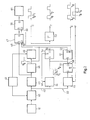
- Fig. 1 shows the functional block diagram of an apparatus according to the invention for measuring capacitance changes.
- a high frequency generator 10 provides sine-waves with constant amplitude and frequency.
- the frequency of the generated HF signals is typically 1 MHz which, depending on the requirements of actual tasks, can be varied freely between about 1 and 30 MHz.
- the output of the HF generator 10 is coupled through a high frequency transformer 11 to the measuring circuit 12.
- the measuring circuit 12 comprises a diode 13 representing the semiconductor junction which is to be measured and a compensating capacitor 14 with adjustable capacitance.
- the HF transformer 11 has a symmetrical secondary winding, and the two end terminals thereof are coupled to the measuring circuit 12, while its central tapping is connected through a controlled switch 15 to either of DC sources 16 or 17 as defined by the actual switching positions.
- the voltage of the DC sources 16 and 17 can be adjusted to correspond to the requirements of the measurement.
- the typical output voltage of the DC source 17 is -10 V which can change between about -0.5 V and -20 V and the typical voltage range of the DC source 16 is between -1 V and +2 V.
- the position of the controlled switch 15 is defined by the value of a control voltage C coupled to its control input.
- the output of the measuring circuit 12 is coupled to a high frequency amplifier 18 providing a predetermined selective gain at the operational frequency of the HF generator 10.
- a second controlled switch 19 is connected to the input of the HF amplifier 18 and depending on the value of a control voltage D coupled to its control input either earths the output of the measuring circuit 12 or isolates the same from the ground.
- a parallel circuit consisting of diode 20 and choke 21 is connected in parallel to the controlled switch between the ground and the output of the measuring circuit 12, in which the choke 21 is used for closing the DC path of the diode 20.
- the controlled switches 15 and 19 can be realized preferably by VMOS FET devices which can be arranged as shown e.g. in Fig. 1 of APPLICATION NOTE AN77-2 of the Company Silicon-ix Semiconductor Devices, or as published in the article of Walt Heinzer: "Don't Trade Off Analog Switch Specs.” (Electronic Design, October 1977).
- the two branches of the controlled switch 15 can be implemented preferably by N and P channel transistors. For such applications good results can be obtained by the VMOS FET devices Type: BD 212 and BD 222 of ITT.
- the output of the HF amplifier 18 is coupled to a phase-sensitive detector 22 having a reference input connected to the output of the HF generator 10.
- the phase of the reference signal of the phase-sensitive detector 22 is adjusted in such a way that the output of the latter represents a DC voltage corresponding to the capacitive voltage component being present at the output of the measuring circuit 12.
- the circuits described hereinabove form substantially a capacitance measuring unit.
- the output signal of this unit is coupled through a transmission gate 23 to the signal input of a low frequency lock-in amplifier 24.
- the transmission gate 23 consists of controlled switches 25 and 26 and of an amplifier 27 with an integrating input coupled between the controlled switches 25 and 26.
- the integrator at the input of the amplifier consists of resistor 28 and capacitor 29.
- the control inputs of the switches 25 and 26 are interconnected and are coupled to a common control voltage E.
- the switches 25 and 26 have always complementary states.
- the lock-in . amplifier 24 conceives the pulsating DC voltage with specific properties (described later) coming from the output of the transmission gate 23 and performs a phase-dependent detection function on the input signal phase-related to a square-wave control voltage F coupled to its square-wave input 30.
- the so obtained DC voltage is recorded by the X channel of an X-Y recorder 31 or fed to any other kind of recorder.
- control voltages C, D, E and F for the controlled switches 15, 19, 25 and 26 and for the lock-in amplifier 24 are generated by a control unit 32 shown in Fig. 2.
- the HF generator 10 provides signals with high frequency stability and constant amplitude (e.g. sine waves of 1 MHz) coupled through the HF transformer 11 to the measuring circuit 12.
- the voltage (e.g. -10 V) of the DC source 17 is coupled to the diode 13 and a voltage minimum is adjusted by the compensating capacitor 14 at the output of the phase-sensitive detector 22.
- the capacitance of the compensating capacitor 14 should be adjustable substantially within the expoected range of the reverse-biased junction capacitance of the test diode which falls typically between 1 pF and 100 pF.
- the measurement of capacitance-changes can be started. The measurement is carried out in accordance with the principle of the DLTS technique referred to hereinbefore, in which the semiconductor to be measured is exposed to various thermal effects. For understanding the measurement process knowledge of the thermal handling of the semiconductor device represented by the diode 13 is not necessary.
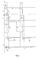
- the control unit 32 is used to provide control voltages by which the states of the controlled switches 15 and 19 are periodically changed as illustrated in diagrams C and D in Fig. 3.
- the duration of period Tp can be adjusted according to actual requirements typically between 2 sec and 0.4 msec.
- the diode 13 receives the voltage of the DC source 16 which is e.g. +1 V and under such a DC voltage its capacitance will be substantially higher than it had been with reverse bias.
- the increase in capacitance can be as high as 2 or 4 decimal orders of magnitude.
- the control pulse C lasts through a period T B and during this time the voltage at the output of the phase-sensitive detector 22 will be as shown in diagram L of Fig. 3.
- control pulse C is composed of a number of shorter pulses within the period T B , which pulses might have even different amplitudes.
- the discrete pulsating excitation offers a possibility e.g. for measuring the capture cross-section not only of the hole but also of the electron of a minority carrier trap.
- the input of the HF amplifier 18 is shunted to earth by the controlled switch 19 during the period T B ; however, the HF signal arriving from the output of the measuring circuit 12 provides even with the grounded amplifier a relatively high voltage response at the output of the phase-sensitive detector 22.
- the controlled switch 15 changes its state and passes the voltage of -10 V of the DC source 17 to the diode 13, and in response to such a bias the capacitance of the diode 13 will rapidly decrease and a corresponding decrease or change in the output voltage of the phase-sensitive detector 22 will be obtained.
- the shunt from the output of the measuring circuit 12 will be released at time t 2 when the controlled switch 19 is operated, and the moment t 2 is delayed by approximately 20 nsec compared to the moment t i . This delay is required due to the fact that the measuring signal can pass to the input of the HF amplifier 18 only when the switching transient processes of the controlled switch 15 have already finished.
- the capacitance of the diode 13 decreases rapidly following the moment t,, and in accordance with the DLTS technique the object of the measurement lies in the correct recording of this capacitance change.
- the voltage at the output of the phase-sensitive detector 22 depends on the difference between the capacitance of the diode 13 and of the compensating capacitor 14 and on the sign of this difference.
- the beginning of the actual measurement period is defined by the moment t 3 determined by the beginning of the square wave coupled to the reference input of the lock-in amplifier 24.
- the control voltage F begins at time t 3 which is delayed by a period T G compared to the starting time to of the control voltage C.
- the frequency of the control voltage F is 1/Tp.
- the time delay T ⁇ is composed of two factors i.e. of the pulse time T. of the control voltage C and of a dead period T H defined between the end moment of the control voltage C and the beginning moment t 3 of the measurement. It should be noted that for illustrating purposes the time scale in Fig. 3, especially between the times to and t 3 , is rather distorted.
- the duration of the period T B is adjustable with a minimum value of about 50 nsec.
- the maximum length of that period depends on the required accuracy and on the repetition frequency.
- the suitable adjustment of the dead period T H is of outstanding importance regarding the reproducibility of different measurements.
- the moment t 3 falls in the rapidly changing section of the capacitance curve, and if the beginning moment of the measuring window is chosen arbitrarily, then the evaluation of data obtained by different measurements carried out with different repetition frequencies might lead to the drawing of incorrect conclusions.
- a basic idea of the present invention lies in that the moment t 3 which defines the beginning of the measurement should be delayed relative to the ending moment t, of the control pulse with such an extent that this delay should represent the same phase shift compared to the control voltage C having a period time Tp and frequency fp.
- the accuracy of the measurement is proportional to the quotient T G /T p . It can be proved that as long as the quotient T s /Tp is smaller than 0.1 the accuracy of the concentration measurement of the examined doping level is better than 1%.
- the response time of the capacitance measuring apparatus shown in Fig. 1 is about 2 psec.
- the response time is the length of the period in which the capacitance following the moment t, decreases from 90% of its value at the moment t, to 10% of the same value.
- the transmission gate 23 protects the signal input of the lock-in amplifier 24 form the high signal amplitude coming out from the output of the phase-sensitive detector 22 during the period T G (Fig. 3 diagram L) which might result in the overdriving of the input circuitry of the lock-in amplifier.
- a signal U M shown in diagram M of Fig, 3 is coupled to the signal input of the lock-in amplifier 24.
- the output of the phase-sensitive detector 22 is coupled by the controlled switch 26 only during the measurement period T M to the input of the lock-in amplifier 24.
- the controlled switches 25 and 26 take the conditions illustrated in Fig. 1 in response to the control voltage E, and in that period the amplifier 27 acts as a track-and-hold type sampling circuit which couples the voltage U M (shown in diagram M of Fig. 3) to the input of the lock-in amplifier 24 through the controlled switch switch 26.
- the integrating member consisting of the resistor 28 and capacitor 29 receives the output signal of the phase-sensitive detector 22. Under real conditions disturbing signals can be superimposed on this output signal as it has been illustrated at section 33 in diagram L of Fig. 3.
- the time constant of about 1 msec of the integrating member provides that the amplifier 27 can receive only the mean value of this output signal averaged for a period of about 1 msec.
- the input of the lock-in amplifier 24 receives the mean value of the rectified measuring signal averaged for a time period of 1 msec directly preceding the moment to and held through the full period T G , and this operation is due to the specific design of the transmission gate 23.
- the design of the transmission gate 23 as a switched track-and-hold stage protects the input of the lock-in amplifier 24 from being overdriven, and the sensitivity and the accuracy of the capacitance measurement is increased by supplying the averaged capacitance value to the lock-in amplifier input during the period T G .
- the various capacitance-change measurements supply evaluable and comparable results even if the period time of the pulses and the pulse-width are changing within wide limits.
- FIG. 2 shows a schematic circuit diagram as an embodiment for the generation of these control voltages which illustrates the control unit 32.
- the HF generator 10 has been indicated also on Fig. 2, and the quartz-controlled output signals of the generator 10 which have a stable frequency are used for the generation of the various control voltages.
- the output of the generator 10 is coupled to a frequency synthesiser 40 which is a conventional unit designed in such a way that in response to the constant frequency signals coupled to its input it generates output pulses having a frequency which is 5000-times higher than the measuring frequency fp which is controlled by a frequency control signal delivered by a handling unit 41.
- the handling unit 41 is used to adjust the measuring frequency fp to a required value between 0.5 Hz and 2.5 kHz.
- the frequency synthesiser 40 is coupled to an output line 42 on which pulses with 5000 fp are present.
- the output line 42 is coupled to counting inputs of counters 43, 44 and 45.
- the counter 43 which in the exemplary embodiment provides a frequency division by 500, is coupled both to the input of a further counter 46 and to set input 48 of a store 47 associated with an error detecting unit.
- the counter 46 provides a frequency division by ten and the 1-0 transitions of the output of the counter 46 determines the starting moments of the control voltage C, i.e. the moment to indicated in Fig. 3.
- the output of the counter 46 is coupled to the starting input of a pulse generator 49 and to the clear input 50 of the store 47 and to the clear input 52 of another store 51.
- the pulse generator 49 is adapted to provide the control voltage C, and for the purpose of setting the duration T B of the voltage pulse C the pulse generator 49 receives a control signal from an appropriate output of the handling unit 41, whereby the width of the voltage pulse C can be adjusted to any required value.
- the upper limit for the adjustment of the duration T B is determined by the fact that the period T G which is closely related to the period T B can be up to a tenth of the period time Tp. This condition is required for attaining the accuracy better than 1 % referred to hereinabove.
- the output of the pulse generator 49 forms the output of the control unit 32 that delivers the control voltage C, and on the other hand it is coupled to the input of a delay member 53.
- the delay member delays the rear 1-0 edge of the control pulse C by a period of about 20 nsec. In this way the output of the delay member 53 provides the control pulses D shown in Fig. 3.
- the output of the pulse generator 49 is coupled additionally to clear input 55 of a store 54.
- the inverted output of the store 54 is connected to the combined enable and clear input 56 of the counter 44.
- the output of the counter 44 is coupled to the set input of the store 54, to the set input of the store 51 and to clear input 58 of a store 57.
- the set input of the store 57 is connected to the output of the counter 45 which carries out a division by 2500.
- the inverted output of the store 57 provides the control voltage F and it is also coupled to the combined enable and clear input of the counter 45.
- the inverter output of the store 51 supplies the pulses of the control voltage E.
- the inverted output of the store 51 is coupled to gating input (clear) 60 of a gated store 59.
- the set input of the store 59 is coupled to the non-inverted output of the store 47, and the output of the store 59 is connected to the input of an error indicating unit 61 comprising preferably indicator lamps.
- the frequency synthesiser 40 supplies pulses having 5000 times as high a frequency as the measuring frequency is, and in response to these pulses the counters 43 and 46, which provide together a combined frequency division by 5000, generate respective 1-0 transition jumps that control the pulse generator 49 in the starting moment to of each pulse of the control voltage C.
- the pulse generator 49 provides the pulses C at its output having a duration T B set by the handling unit 41.
- the delay member 53 delays the rear edge of the pulse C, whereby the pulse D of the control voltage D is obtained.
- the 1-0 transition of the pulse C occurring in the moment t 1 clears the store 54 and the inverted output of the store 54 enables the counting operation for the counter 44 that carries out a division by 200.
- the store 54 In response to such a control the store 54 is set, it stops the enable condition of the counter 44 and resets the same, turns the store 51 into the set condition to deliver a 1-0 transition at its inverted output at the moment t 3 , and the store preserves its set condition (0 at its inverted output) till the moment to of the next period. In such a way the inverted output of the store 51 provides the pulse of the control voltage E.
- the 1-0 transition at the output of the counter 44 occurring in the moment t 3 will additionally clear the store 57 which responds by a 0-1 jump at its inverted output corresponding to the starting 0-1 jump of the control voltage F.
- This jump at the inverted output of the store 57 enables the counting operation of the counter 45 implementing a frequency division by 2500, and the output of the counter 45 provides a jump in the moment t 4 occurring after the 2500th pulse following the moment t 3 , to set the store 57.
- the changed state of the store 57 results in a corresponding change at the output of the control voltage F.
- control voltage F is provided by an appropriate pulse-forming circuit (not shown in the drawing) coupled to the inverted output of the store 57.
- the non-inverted output of the store 47 is in 0 state during the first 10% of the period time Tp which is followed by a 1 state in the remaining part of the period.
- the store 59 is designed in such a way, that the transition coupled to its gating input 60 at the moment t 3 can change its state only if the moment t 3 occurs later than the end of the 0.1 Tp period following the moment to when the output of the store 47 takes a logical 1 state.
- the error indicating unit 61 indicates the change of the state of the store 59 for the operator to adjust a shorter pulse duration by the handling unit 41.
- control unit 32 can supply all the control voltages required for the operation of the capacitance-change measuring apparatus shown in Fig. 1.
Landscapes
- Physics & Mathematics (AREA)
- General Physics & Mathematics (AREA)
- Investigating Or Analyzing Materials By The Use Of Electric Means (AREA)
- Measurement Of Resistance Or Impedance (AREA)
- Testing Of Individual Semiconductor Devices (AREA)
- Testing Or Measuring Of Semiconductors Or The Like (AREA)
Description
- The invention relates to deep level transient spectroscopy (DLTS) and more particularly to a method for carrying out DLTS scanning on a semiconductor junction by measuring a predetermined sequence of the transient capacitance changes of the junction. The invention relates also to an apparatus for carrying out the method.
- It is well-known in the art that by the measurement of the capacitance change versus time curves of the depletion region or space charge layer near PN junctions in semiconductor devices the concentration, activation energy, thermal and optical capture cross-sections of localized states (created by foreign atoms, point defects, dialocations, etc.) in the forbidden band of the semiconductor devices can be determined.
- The change of the occupancy of the localized states in the forbidden band can be measured as a change of the capacitance. During such measurements the localized states are periodically filled and emptied, and the amplitude of the resulting periodical capacitance change is determined by the concentration of the energy states, while the kinetics thereof is determined by the activation energies and thermal capture cross-sections of the localized states as a function of temperature.
- The occupancy of the localized states are changed by voltage-, current- or light-pulses applied to the PN junction. This measuring method is the deep level transient spectroscopy or DLTS method as referred to hereinabove, and instruments utilising this method are indispensable factors in development and quality control work in the field of semiconductor devices.
- The DLTS method is described in the paper of G. L. Miller, D. V. Lang and L. C. Kimberling entitled "Capacitance Transient Spectroscopy" (Ann. Rev. Mater. Sci. 1977, pp 377-448) and here the authors also give a survey of the instrumentation used for the measurement of transient capacitance changes.
- The measurement of the capacitance changes is carried out in such a way that the diode representing the semiconductor junction to be measured is connected into one arm of a bridge, and a compensating capacitance is inserted in the other arm of the bridge having a capacitance equal to that of the diode. A high frequency signal is applied to the two arms of the bridge through a symmetrical high frequency transformer.
- In addition to the application of the high frequency signal a train of pulses is applied to the diode through a pulse transformer. The repetition rate and the duty cycle of the pulsers can be adjusted within wide ranges in accordance with the DLTS method. During the occurrence of the pulses a forward or slightly reverse voltage is applied to the diode, and between the ending moments of the pulses and the starting moments of the subsequent pulses a high reverse voltage is applied to the diode. The capacitance of the diode is substantially different under the two kinds of voltages applied thereto which difference can be as high as 2-3 decimal orders of magnitude, and during the presence of the reverse bias a capacitance transient (a decay) takes place which is typically by 4 decimal orders of magnitude smaller than the d.c. reverse capacitance.
- The task of the measurement is to determine the small capacitance changes during the reverse biasing pulses.
- In the known measuring apparatus the output of the measuring circuit is detected by a phase-sensitive detector following a sufficient amplification, and the so obtained pulsating voltage will be proportional to the capacitive output signal component of the measuring circuit. This voltage is applied to the input of a low-frequency lock-in amplifier synchronized to the starting moments of the measuring periods, and the second lock-in amplifier selects the component from the rectified pulsating input voltage which has the same frequency as the measuring periods have.
- During performance of the DLTS method the temperature and other parameters of the diode to be measured are changed and such changes take place much slower than the rate of pulses applied to the diode. The information characterizing the properties of the diode is carried by the recorded sequence of capacitance changes obtained during the pulse periods with reverse bias.
- There are a number of problems connected with the known apparatus summarized above.
- The application of the excitation pulses is rather complicated, and in the described arrangement the stray capacitance and series inductance of the pulse transformer can result in pulse parameters other than the set values, especially if there are high conductive losses. The true transmission of pulses with durations that can be varied within a wide range, which wide range is required for the measurement of the capture cross-section of majority or minority carriers, can be solved precisely only by using a plurality of pulse transformers.
- The measuring amplifier receives the full driving signal, and following the significant overloading it can recover relatively slowly, i.e. the ineffective dead period of the capacitance measurement will be long, i.e. the starting section of the exponentially decaying capacitance signal will be lost from the measurement, which all result in a substantially decreased signal to noise ratio compared to an ideal case. If the starting of the reference signal of the low-frequency lock-in amplifier is in fixed time relation to the starting or ending moments of the biasing pulses, then the dead periods will have different lengths when the width and repetition rate of the pulses are changed, which results in inaccurate determinations of activation energies (D. S. Day et al. Journal of Applied Physics, 50/8, 5093/1979).
- High sensitivity can be reached by averaging throughout a long period of time defined generally by the integrating time-constant of the low frequency lock-in amplifier. If the high-frequency gain is high, the high-frequency phase-sensitive detector, which can have only a short time constant for the sake of good transient response, might overdrive the low frequency lock-in amplifier that has a long time constant and a corresponding long recovery period following an overdriving. In order to overcome such unwanted side-effects, neither the high-frequency, nor the low frequency gain can be sufficiently high, i.e. the sensitivity of the capacitance measurements cannot be increased as itwould be desirable.
- The primary object of the invention is to improve the DLTS method in such a way that the measurements carried out by different excitation pulses can be compared to each other unambiguously.
- A further object of the invention is to provide an apparatus for carrying out the DLTS method, which is free from the limitations coming from the application of pulse transformers and in which the overloading of the stages following the measuring circuits can be avoided during the duration of the pulses.
- According to a feature of the invention the measurements carried out with different pulse repetition rates will be comparable with each other if following the ending moments of the pulses the respective measuring periods are started in constant phase positions relative to the pulse repetition waveform. This condition means substantially that the length of the dead periods form a constant portion of the period of the pulses.
- Thus the invention provides a method of investigating a semiconductor junction having traps in the neighbourhood thereof by deep level transient spectroscopy scanning, said method comprising the steps of:
- (a) applying to the junction a high frequency signal;
- (b) simultaneously applying to the junction a bias voltage which is alternatively and repetitively switched from a first voltage level biasing the junction in a forward or reverse direction to second voltage level providing a reverse bias stronger than that of the first level, the repetition period of said switching being substantially longer than the period of the high frequency signal;
- (c) detecting the amplitude envelope of the capacitive signal component of said high frequency signal after switching to the second voltage level and applying the detected amplitude envelope to a lock-in amplifier;
- (d) supplying the lock-in amplifier with a synchronising signal in the form of a symmetrical square wave signal having a period of the same duration as the said repetition period but being phase-delayed in respect thereof in such a way that a dead period elapses between the switching to the second voltage level and the start of the square wave signal, the output of the lock-in amplifier representing the transient capacitance change of the junction resulting from the switching of the bias voltage;
- (e) recording said output as a function of the junction temperature or the length of the repetition period or the time interval for which the first voltage level is applied; characterized in that;
- (f) when applying said first voltage level to the junction and during the subsequent dead period, the lock-in amplifier is supplied with a simulated envelope signal coresponding in magnitude to the envelope signal existing prior to the application of the first voltage level;
- (g) the length of said dead period is adjusted to always form a predetermined fraction of the repetition period whatever the length of this period is.
- In the preferred apparatus according to the invention the application of the pulse transformers has been omitted and the pulses are coupled through controlled switches driven by a control unit to the diode to be measured.
- The invention also provides an apparatus for carrying out the method as defined above, comprising:
- (a) means for generating a high frequency signal;
- (b) a bridge circuit including:
- (i) a centrally tapped winding constituting the secondary winding of a transformer excited by said high frequency signal;
- (ii) two branches having first ends connected to opposite terminals of the secondary winding and second ends interconnected with each other, one of said branches containing the junction under test and the other containing a variable reference capacitance;
- (c) means for applying to said junction, alternatingly and with a predetermined repetition period, a first voltage level biasing the junction in a forward or a reverse direction and a second voltage level providing a reverse bias stronger than that of the first level, said repetition period being substantially longer than the period of the high frequency signal;
- (d) a high frequency amplifier connected to the connection of the second ends of said branches;
- (e) a phase-sensitive detector receiving the output signal from the high frequency amplifier and, as a reference signal, the high frequency signal, and providing at its output the amplitude envelope of the signal emerging from the high frequency amplifier;
- (f) a lock-in amplifier receiving the envelope signal from the phase sensitive detector and, as a synchronising signal, a symmetrical square wave signal having a period of the same duration as the said repetition period but being phase-delayed in respect thereof in such a way that a dead period elapses between the termination of the first voltage level and the start of the square wave signal;
- (g) means for recording the output from the lock-in amplifier as a function of the junction temperature or the length of the repetition period or the time interval for which the first voltage level is applied; characterized by
- (h) means for providing to the lock-in amplifier, instead of the envelope signal, a simulated envelope signal while the first voltage level is provided to the junction and also during subsequent dead-period, said simulated envelope signal corresponding in magnitude to the envelope signal corresponding in magnitude to the envelope signal existing prior to the application of the first voltage level;
- (i) a control unit adapted to control the phase-delay between the repetition period and the period of the square wave signal in such a manner that the length of the dead period is always a predetermined fraction of the repetition period, whatever the length of said period is.
- In order to prevent the lock-in amplifier from being overdriven and to simulate the missing measuring signal during the pulses, between the output of the high frequency phase-sensitive amplifier and the input of the low frequency lock-in amplifier a track-and-hold type integrating amplifier is coupled through respective controlled switches, and the measuring signals are passed only in the reepctive measuring periods to the input of the lock-in amplifier. Between the measuring periods a simulated (reconstructed) measuring signal is passed from the gated integrating amplifier to the input of the lock-in amplifier, in which the voltage of the simulated signal corresponds to the average of the measuring signal in the end section of the previous measuring period.
- An embodiment of the invention will now be described by way of example and with reference to the accompanying drawings, in which:
- Fig. 1 shows the block diagram of an embodiment of the apparatus according to the invention,
- Fig. 2 shows the detailed block diagram of the
control unit 32 shown in Fig. 1, and - Fig. 3 shows the time diagrams at various points of the apparatus shown in Figs. 1 and 2.
- Fig. 1 shows the functional block diagram of an apparatus according to the invention for measuring capacitance changes. A
high frequency generator 10 provides sine-waves with constant amplitude and frequency. The frequency of the generated HF signals is typically 1 MHz which, depending on the requirements of actual tasks, can be varied freely between about 1 and 30 MHz. The output of theHF generator 10 is coupled through ahigh frequency transformer 11 to the measuringcircuit 12. The measuringcircuit 12 comprises a diode 13 representing the semiconductor junction which is to be measured and a compensatingcapacitor 14 with adjustable capacitance. TheHF transformer 11 has a symmetrical secondary winding, and the two end terminals thereof are coupled to the measuringcircuit 12, while its central tapping is connected through a controlledswitch 15 to either ofDC sources DC sources DC source 17 is -10 V which can change between about -0.5 V and -20 V and the typical voltage range of theDC source 16 is between -1 V and +2 V. The position of the controlledswitch 15 is defined by the value of a control voltage C coupled to its control input. The output of the measuringcircuit 12 is coupled to ahigh frequency amplifier 18 providing a predetermined selective gain at the operational frequency of theHF generator 10. - A second controlled
switch 19 is connected to the input of theHF amplifier 18 and depending on the value of a control voltage D coupled to its control input either earths the output of the measuringcircuit 12 or isolates the same from the ground. A parallel circuit consisting ofdiode 20 and choke 21 is connected in parallel to the controlled switch between the ground and the output of the measuringcircuit 12, in which thechoke 21 is used for closing the DC path of thediode 20. - The controlled switches 15 and 19 can be realized preferably by VMOS FET devices which can be arranged as shown e.g. in Fig. 1 of APPLICATION NOTE AN77-2 of the Company Silicon-ix Semiconductor Devices, or as published in the article of Walt Heinzer: "Don't Trade Off Analog Switch Specs." (Electronic Design, October 1977). The two branches of the controlled
switch 15 can be implemented preferably by N and P channel transistors. For such applications good results can be obtained by the VMOS FET devices Type: BD 212 and BD 222 of ITT. - The output of the
HF amplifier 18 is coupled to a phase-sensitive detector 22 having a reference input connected to the output of theHF generator 10. The phase of the reference signal of the phase-sensitive detector 22 is adjusted in such a way that the output of the latter represents a DC voltage corresponding to the capacitive voltage component being present at the output of the measuringcircuit 12. - The circuits described hereinabove form substantially a capacitance measuring unit. The output signal of this unit is coupled through a
transmission gate 23 to the signal input of a low frequency lock-inamplifier 24. Thetransmission gate 23 consists of controlledswitches amplifier 27 with an integrating input coupled between the controlled switches 25 and 26. The integrator at the input of the amplifier consists ofresistor 28 andcapacitor 29. The control inputs of theswitches - The lock-in.
amplifier 24 conceives the pulsating DC voltage with specific properties (described later) coming from the output of thetransmission gate 23 and performs a phase-dependent detection function on the input signal phase-related to a square-wave control voltage F coupled to its square-wave input 30. The so obtained DC voltage is recorded by the X channel of anX-Y recorder 31 or fed to any other kind of recorder. - The control voltages C, D, E and F for the controlled switches 15, 19, 25 and 26 and for the lock-in
amplifier 24 are generated by acontrol unit 32 shown in Fig. 2. - The operation of the capacitance-change measuring apparatus shown in Fig. 1 will now be described with reference to the time diagrams of Fig. 3.
- As already mentioned, the
HF generator 10 provides signals with high frequency stability and constant amplitude (e.g. sine waves of 1 MHz) coupled through theHF transformer 11 to the measuringcircuit 12. Before the beginning of a measurement the voltage (e.g. -10 V) of theDC source 17 is coupled to the diode 13 and a voltage minimum is adjusted by the compensatingcapacitor 14 at the output of the phase-sensitive detector 22. The capacitance of the compensatingcapacitor 14 should be adjustable substantially within the expoected range of the reverse-biased junction capacitance of the test diode which falls typically between 1 pF and 100 pF. After balancing the measuringcircuit 12 the measurement of capacitance-changes can be started. The measurement is carried out in accordance with the principle of the DLTS technique referred to hereinbefore, in which the semiconductor to be measured is exposed to various thermal effects. For understanding the measurement process knowledge of the thermal handling of the semiconductor device represented by the diode 13 is not necessary. - The
control unit 32 is used to provide control voltages by which the states of the controlled switches 15 and 19 are periodically changed as illustrated in diagrams C and D in Fig. 3. The duration of period Tp can be adjusted according to actual requirements typically between 2 sec and 0.4 msec. During the occurrence of the control voltage C the diode 13 receives the voltage of theDC source 16 which is e.g. +1 V and under such a DC voltage its capacitance will be substantially higher than it had been with reverse bias. The increase in capacitance can be as high as 2 or 4 decimal orders of magnitude. The control pulse C lasts through a period TB and during this time the voltage at the output of the phase-sensitive detector 22 will be as shown in diagram L of Fig. 3. The essence of the measurement method will not be affected if the control pulse C is composed of a number of shorter pulses within the period TB, which pulses might have even different amplitudes. The discrete pulsating excitation offers a possibility e.g. for measuring the capture cross-section not only of the hole but also of the electron of a minority carrier trap. The input of theHF amplifier 18 is shunted to earth by the controlledswitch 19 during the period TB; however, the HF signal arriving from the output of the measuringcircuit 12 provides even with the grounded amplifier a relatively high voltage response at the output of the phase-sensitive detector 22. - When the control voltage C is finished at time t,, the controlled
switch 15 changes its state and passes the voltage of -10 V of theDC source 17 to the diode 13, and in response to such a bias the capacitance of the diode 13 will rapidly decrease and a corresponding decrease or change in the output voltage of the phase-sensitive detector 22 will be obtained. The shunt from the output of the measuringcircuit 12 will be released at time t2 when the controlledswitch 19 is operated, and the moment t2 is delayed by approximately 20 nsec compared to the moment ti. This delay is required due to the fact that the measuring signal can pass to the input of theHF amplifier 18 only when the switching transient processes of the controlledswitch 15 have already finished. The capacitance of the diode 13 decreases rapidly following the moment t,, and in accordance with the DLTS technique the object of the measurement lies in the correct recording of this capacitance change. - The voltage at the output of the phase-sensitive detector 22 (diagram L in Fig. 3) depends on the difference between the capacitance of the diode 13 and of the compensating
capacitor 14 and on the sign of this difference. - The beginning of the actual measurement period is defined by the moment t3 determined by the beginning of the square wave coupled to the reference input of the lock-in
amplifier 24. The control voltage F begins at time t3 which is delayed by a period TG compared to the starting time to of the control voltage C. The frequency of the control voltage F is 1/Tp. The time delay Tα is composed of two factors i.e. of the pulse time T. of the control voltage C and of a dead period TH defined between the end moment of the control voltage C and the beginning moment t3 of the measurement. It should be noted that for illustrating purposes the time scale in Fig. 3, especially between the times to and t3, is rather distorted. - The duration of the period TB is adjustable with a minimum value of about 50 nsec. The maximum length of that period depends on the required accuracy and on the repetition frequency. The suitable adjustment of the dead period TH is of outstanding importance regarding the reproducibility of different measurements. The moment t3 falls in the rapidly changing section of the capacitance curve, and if the beginning moment of the measuring window is chosen arbitrarily, then the evaluation of data obtained by different measurements carried out with different repetition frequencies might lead to the drawing of incorrect conclusions.
- A basic idea of the present invention lies in that the moment t3 which defines the beginning of the measurement should be delayed relative to the ending moment t, of the control pulse with such an extent that this delay should represent the same phase shift compared to the control voltage C having a period time Tp and frequency fp. This statement is equivalent to the definition that in case of any frequency fp the equation:

- The useful measuring period TM = Tp―Tg, wherein TG = TB+TH.
- The accuracy of the measurement is proportional to the quotient TG/Tp. It can be proved that as long as the quotient Ts/Tp is smaller than 0.1 the accuracy of the concentration measurement of the examined doping level is better than 1%. With such data if the repetition frequency is chosen to be fp = 2 kHz, the pulse width of the control voltage can be TB = 30 µsec and if the frequency is decreased to Fp = 50 Hz, the pulse width can be increased to TB = 1.2 msec with the same accuracy of 1%.
- According to the above conditions the length of the dead period TH should be adjusted to be proportional to the period time Tp. The response time of the capacitance measuring apparatus shown in Fig. 1 is about 2 psec. By way of definition the response time is the length of the period in which the capacitance following the moment t, decreases from 90% of its value at the moment t, to 10% of the same value. In order to reach the original capacitance value (with reverse bias) with an accuracy of ΔC/C = 10-4, eight times as much time should be waited for the beginning of the measuring period i.e. the waiting period is 16 µsec. This period is called a settling time. If the maximum of the repetition frequency fp = 2.5 kHz, then the settling time of 16 µsec is 1/25th part of the period time Tp corresponding to this frequency. This explains the
value 25 for k. - The
transmission gate 23 protects the signal input of the lock-inamplifier 24 form the high signal amplitude coming out from the output of the phase-sensitive detector 22 during the period TG (Fig. 3 diagram L) which might result in the overdriving of the input circuitry of the lock-in amplifier. During the period TG a signal UM shown in diagram M of Fig, 3 is coupled to the signal input of the lock-inamplifier 24. The output of the phase-sensitive detector 22 is coupled by the controlledswitch 26 only during the measurement period TM to the input of the lock-inamplifier 24. During the period TG the controlled switches 25 and 26 take the conditions illustrated in Fig. 1 in response to the control voltage E, and in that period theamplifier 27 acts as a track-and-hold type sampling circuit which couples the voltage UM (shown in diagram M of Fig. 3) to the input of the lock-inamplifier 24 through the controlledswitch switch 26. - During the measurement period Tm the integrating member consisting of the
resistor 28 andcapacitor 29 receives the output signal of the phase-sensitive detector 22. Under real conditions disturbing signals can be superimposed on this output signal as it has been illustrated atsection 33 in diagram L of Fig. 3. The time constant of about 1 msec of the integrating member provides that theamplifier 27 can receive only the mean value of this output signal averaged for a period of about 1 msec. During the period TG the input of the lock-inamplifier 24 receives the mean value of the rectified measuring signal averaged for a time period of 1 msec directly preceding the moment to and held through the full period TG, and this operation is due to the specific design of thetransmission gate 23. - By the above described operation of the apparatus shown in Fig. 1 many of the technical limitations of the previously used DLTS methods can be overcome. Of the advantages outstanding significance can be attributed to the direct application of the switched pulse-like excitation signal to the measuring
circuit 12 without using a pulse transformer, whereby the pulse durations which have substantial influence on the measurements can be adjusted precisely within wide ranges. The application of switching elements implemented by VMOS FET switching devices does not influence the capacitance prevailing at the measuringcircuit 12. By using the controlledswitch 19 to short-circuit the input of theHF amplifier 18 and the following phase-sensitive detector 22 during the period TB of the control voltage C, the overdriving of these stages is prevented or the realization of higher gain is made possible during the measurement period TM. The design of thetransmission gate 23 as a switched track-and-hold stage protects the input of the lock-inamplifier 24 from being overdriven, and the sensitivity and the accuracy of the capacitance measurement is increased by supplying the averaged capacitance value to the lock-in amplifier input during the period TG. - When after the end of the pulse C of the control voltage the measurement period TM is started always in identical phase conditions relative to the period time of the pulses, the various capacitance-change measurements supply evaluable and comparable results even if the period time of the pulses and the pulse-width are changing within wide limits.
- For the operation of the apparatus shown in Fig. 1, the generation of the control voltages C, D, E and F will be necessary. Fig. 2 shows a schematic circuit diagram as an embodiment for the generation of these control voltages which illustrates the
control unit 32. - The
HF generator 10 has been indicated also on Fig. 2, and the quartz-controlled output signals of thegenerator 10 which have a stable frequency are used for the generation of the various control voltages. The output of thegenerator 10 is coupled to afrequency synthesiser 40 which is a conventional unit designed in such a way that in response to the constant frequency signals coupled to its input it generates output pulses having a frequency which is 5000-times higher than the measuring frequency fp which is controlled by a frequency control signal delivered by ahandling unit 41. Thehandling unit 41 is used to adjust the measuring frequency fp to a required value between 0.5 Hz and 2.5 kHz. Thefrequency synthesiser 40 is coupled to anoutput line 42 on which pulses with 5000 fp are present. Theoutput line 42 is coupled to counting inputs ofcounters counter 43 which in the exemplary embodiment provides a frequency division by 500, is coupled both to the input of afurther counter 46 and to setinput 48 of astore 47 associated with an error detecting unit. Thecounter 46 provides a frequency division by ten and the 1-0 transitions of the output of thecounter 46 determines the starting moments of the control voltage C, i.e. the moment to indicated in Fig. 3. The output of thecounter 46 is coupled to the starting input of apulse generator 49 and to theclear input 50 of thestore 47 and to theclear input 52 of anotherstore 51. - The
pulse generator 49 is adapted to provide the control voltage C, and for the purpose of setting the duration TB of the voltage pulse C thepulse generator 49 receives a control signal from an appropriate output of thehandling unit 41, whereby the width of the voltage pulse C can be adjusted to any required value. The upper limit for the adjustment of the duration TB is determined by the fact that the period TG which is closely related to the period TB can be up to a tenth of the period time Tp. This condition is required for attaining the accuracy better than 1 % referred to hereinabove. - The output of the
pulse generator 49 forms the output of thecontrol unit 32 that delivers the control voltage C, and on the other hand it is coupled to the input of adelay member 53. The delay member delays the rear 1-0 edge of the control pulse C by a period of about 20 nsec. In this way the output of thedelay member 53 provides the control pulses D shown in Fig. 3. The output of thepulse generator 49 is coupled additionally to clearinput 55 of astore 54. The inverted output of thestore 54 is connected to the combined enable andclear input 56 of thecounter 44. In the exemplary embodiment thecounter 44 provides a frequency division by 200, and it delivers at its output a 1-0 edge when it receives the 200th control pulse following the incoming of the enabling spike. Since the output of thefrequency synthesiser 40 supplies round 5000 control pulses to thecounter 44 during the period time Tp, the frequency division by 200 realized by thecounter 44 implements a delay of TH = Tp/25 represented by the 1-0 transition of its output. - The output of the
counter 44 is coupled to the set input of thestore 54, to the set input of thestore 51 and to clearinput 58 of astore 57. The set input of thestore 57 is connected to the output of thecounter 45 which carries out a division by 2500. The inverted output of thestore 57 provides the control voltage F and it is also coupled to the combined enable and clear input of thecounter 45. - The inverter output of the
store 51 supplies the pulses of the control voltage E. The inverted output of thestore 51 is coupled to gating input (clear) 60 of agated store 59. The set input of thestore 59 is coupled to the non-inverted output of thestore 47, and the output of thestore 59 is connected to the input of anerror indicating unit 61 comprising preferably indicator lamps. - The operation of the
contol unit 32 shown in Fig. 2 is as follows. - The
frequency synthesiser 40 supplies pulses having 5000 times as high a frequency as the measuring frequency is, and in response to these pulses thecounters pulse generator 49 in the starting moment to of each pulse of the control voltage C. Thepulse generator 49 provides the pulses C at its output having a duration TB set by thehandling unit 41. Thedelay member 53 delays the rear edge of the pulse C, whereby the pulse D of the control voltage D is obtained. - The 1-0 transition of the pulse C occurring in the moment t1 clears the
store 54 and the inverted output of thestore 54 enables the counting operation for thecounter 44 that carries out a division by 200. The output of thecounter 44 provides an 1-0 transition when a time period of TH = Tp/25 hs elapsed since the moment tj, and this 1-0 transition controls the set inputs of thestores clear input 58 of thestore 57. This transition occurs at the momentt3 (Fig. 3). In response to such a control thestore 54 is set, it stops the enable condition of thecounter 44 and resets the same, turns thestore 51 into the set condition to deliver a 1-0 transition at its inverted output at the moment t3, and the store preserves its set condition (0 at its inverted output) till the moment to of the next period. In such a way the inverted output of thestore 51 provides the pulse of the control voltage E. The 1-0 transition at the output of thecounter 44 occurring in the moment t3 will additionally clear thestore 57 which responds by a 0-1 jump at its inverted output corresponding to the starting 0-1 jump of the control voltage F. This jump at the inverted output of thestore 57 enables the counting operation of thecounter 45 implementing a frequency division by 2500, and the output of thecounter 45 provides a jump in the moment t4 occurring after the 2500th pulse following the moment t3, to set thestore 57. The changed state of thestore 57 results in a corresponding change at the output of the control voltage F. - It should be noted that the square-
wave input 30 of the lock-inamplifier 24 requires bipolar pulses, therefore the control voltage F is provided by an appropriate pulse-forming circuit (not shown in the drawing) coupled to the inverted output of thestore 57. - During the time-period of Tp following the moment to the
store 47 is in reset condition, because at the moment to its clear input is actuated, and itsset input 48 will be actuated by the output of thecounter 43 when the time-period ofT pi1 has elapsed. Thus the non-inverted output of thestore 47 is in 0 state during the first 10% of the period time Tp which is followed by a 1 state in the remaining part of the period. Thestore 59 is designed in such a way, that the transition coupled to itsgating input 60 at the moment t3 can change its state only if the moment t3 occurs later than the end of the 0.1 Tp period following the moment to when the output of thestore 47 takes a logical 1 state. This means that the turning on of thestore 59 occurs only in cases when the period TG shown in Fig. 3 is longer than 10% of the full period time Tp. Theerror indicating unit 61 indicates the change of the state of thestore 59 for the operator to adjust a shorter pulse duration by thehandling unit 41. - It can be seen from the above description that the
control unit 32 can supply all the control voltages required for the operation of the capacitance-change measuring apparatus shown in Fig. 1.
Claims (8)
Applications Claiming Priority (2)
| Application Number | Priority Date | Filing Date | Title |
|---|---|---|---|
| HU80801439A HU181136B (en) | 1980-06-07 | 1980-06-07 | Method and instrument for measuring change in transient capacity of semiconducting elements |
| HU143980 | 1980-06-07 |
Publications (2)
| Publication Number | Publication Date |
|---|---|
| EP0041858A1 EP0041858A1 (en) | 1981-12-16 |
| EP0041858B1 true EP0041858B1 (en) | 1986-10-01 |
Family
ID=10954511
Family Applications (1)
| Application Number | Title | Priority Date | Filing Date |
|---|---|---|---|
| EP81302531A Expired EP0041858B1 (en) | 1980-06-07 | 1981-06-08 | Method and apparatus for deep level transient spectroscopy scanning |
Country Status (6)
| Country | Link |
|---|---|
| US (1) | US4437060A (en) |
| EP (1) | EP0041858B1 (en) |
| JP (1) | JPS5724546A (en) |
| DD (1) | DD155655A5 (en) |
| DE (1) | DE3175400D1 (en) |
| HU (1) | HU181136B (en) |
Families Citing this family (17)
| Publication number | Priority date | Publication date | Assignee | Title |
|---|---|---|---|---|
| FR2514903A1 (en) * | 1981-10-21 | 1983-04-22 | Centre Nat Rech Scient | IMPEDANCE MEASURING DEVICE |
| HU182777B (en) * | 1981-11-09 | 1984-03-28 | Mta Mueszaki Fiz Kutato Inteze | Method for determining the charged energy states of semiconductors and insulators by transient spetroscopy of deep equipotential surfaces and device for carrying out the method |
| EP0117259B1 (en) * | 1983-02-23 | 1987-05-06 | Magyar Tudományos Akadémia Müszaki Fizikai Kutato Intézete | A method for determining charged energy states of semiconductor or insulator materials by using deep level transient spectroscopy, and an apparatus for carrying out the method |
| DE3516569A1 (en) * | 1985-05-08 | 1986-11-13 | Rainer Prof. Dr. 3500 Kassel Kassing | BRIDGE FOR THE ABSOLUTE MEASUREMENT OF CAPACITY AND CONDUCTIVE VALUE OF SEMICONDUCTOR SAMPLES |
| JPS63168868U (en) * | 1987-04-23 | 1988-11-02 | ||
| NL8702373A (en) * | 1987-10-05 | 1989-05-01 | Imec Inter Uni Micro Electr | SYSTEM FOR MEASURING STATE DENSITY IN A SEMICONDUCTOR ELEMENT AND METHOD THEREFOR |
| US5042299A (en) * | 1990-07-23 | 1991-08-27 | Iimorrow, Inc. | Capacitive fluid level sensor |
| JP2702807B2 (en) * | 1990-08-09 | 1998-01-26 | 東芝セラミックス株式会社 | Method and apparatus for measuring deep impurity level in semiconductor |
| JP2943474B2 (en) * | 1992-01-20 | 1999-08-30 | 日本電気株式会社 | Waveform analysis method |
| US5521839A (en) * | 1993-09-02 | 1996-05-28 | Georgia Tech Research Corporation | Deep level transient spectroscopy (DLTS) system and method |
| US5701554A (en) * | 1994-06-10 | 1997-12-23 | Seiko Epson Corporation | Fixing apparatus having controller for setting a target temperature and for estimating the amount of heat transferred to a pressure roller |
| US6057701A (en) * | 1998-03-26 | 2000-05-02 | Kolev; Plamen Vassilev | Constant resistance deep level transient spectroscopy (CR-DLTS) system and method, averging methods for DLTS, and apparatus for carrying out the methods |
| US8290726B2 (en) * | 2010-04-28 | 2012-10-16 | Raytheon Company | Photoconductive photodiode built-in test (BIT) |
| JP5817236B2 (en) | 2011-06-17 | 2015-11-18 | 株式会社Sumco | Method for evaluating metal contamination in semiconductor sample and method for manufacturing semiconductor substrate |
| CN102944588A (en) * | 2012-11-23 | 2013-02-27 | 中国科学院微电子研究所 | A method for measuring the interface state parameters induced by etching of AlGaN materials with high Al composition |
| CN111766499B (en) * | 2020-07-28 | 2022-11-25 | 哈尔滨工业大学 | System and method for testing deep energy level transient spectrum of semiconductor material |
| CN111707922B (en) * | 2020-07-28 | 2023-03-14 | 哈尔滨工业大学 | A pulse-triggered deep-level transient spectrum testing system and method |
Family Cites Families (3)
| Publication number | Priority date | Publication date | Assignee | Title |
|---|---|---|---|---|
| US3859595A (en) | 1973-12-06 | 1975-01-07 | Bell Telephone Labor Inc | Method for measuring traps in semiconductors |
| DE2631783C3 (en) | 1976-07-15 | 1979-03-29 | Fraunhofer-Gesellschaft Zur Foerderung Der Angewandten Forschung E.V., 8000 Muenchen | Measuring method for the analysis of traps in semiconductor materials |
| JPS5810853B2 (en) * | 1979-07-03 | 1983-02-28 | 島田理化工業株式会社 | Method for measuring deep impurity levels in semiconductors |
-
1980
- 1980-06-07 HU HU80801439A patent/HU181136B/en unknown
- 1980-12-22 DD DD80226420A patent/DD155655A5/en not_active IP Right Cessation
-
1981
- 1981-06-03 US US06/269,903 patent/US4437060A/en not_active Expired - Lifetime
- 1981-06-06 JP JP8636481A patent/JPS5724546A/en active Pending
- 1981-06-08 DE DE8181302531T patent/DE3175400D1/en not_active Expired
- 1981-06-08 EP EP81302531A patent/EP0041858B1/en not_active Expired
Non-Patent Citations (1)
| Title |
|---|
| Ann. Rev. Mater. Sci. 1977 pages 377-448 * |
Also Published As
| Publication number | Publication date |
|---|---|
| EP0041858A1 (en) | 1981-12-16 |
| DE3175400D1 (en) | 1986-11-06 |
| US4437060A (en) | 1984-03-13 |
| HU181136B (en) | 1983-06-28 |
| JPS5724546A (en) | 1982-02-09 |
| DD155655A5 (en) | 1982-06-23 |
Similar Documents
| Publication | Publication Date | Title |
|---|---|---|
| US4437060A (en) | Method for deep level transient spectroscopy scanning and apparatus for carrying out the method | |
| EP0250683B1 (en) | Tracking sample and hold phase detector | |
| USRE29918E (en) | Contactless LSI junction leakage testing method | |
| JPS6150033A (en) | Time domain reflectometer | |
| EP0067796B1 (en) | Device for indicating pole-zero cancellation, in particular for amplifiers for ionizing radiation spectroscopy | |
| RU2178893C1 (en) | Process determining thermal resistance of junction-package of semiconductor diodes | |
| US4038568A (en) | Pulse peak sample and hold circuit | |
| US3296523A (en) | Apparatus for measuring characteristics of materials through the application of pulses of successively increasing amplitude | |
| EP0209236B1 (en) | Electron beam testing of integrated circuits | |
| US4634972A (en) | Method for measuring low-frequency signal progressions with an electron probe inside integrated circuits | |
| Cova et al. | Digital microspectrofluorometry by multichannel scaling and single photon detection | |
| US4571541A (en) | Method for determining charged energy states of semiconductor or insulator materials by using deep level transient spectroscopy, and an apparatus for carrying out the method | |
| US3445167A (en) | Optical sampling scope-stroboscope using a pulsed laser | |
| EP0268455B1 (en) | Optical detector storage effects reduction | |
| EP0117259B1 (en) | A method for determining charged energy states of semiconductor or insulator materials by using deep level transient spectroscopy, and an apparatus for carrying out the method | |
| CN113701879B (en) | Time-dependent single photon counting circuit and system and method thereof | |
| JPH028732A (en) | Cyclic signal recording method and apparatus | |
| US3475683A (en) | Method and apparatus for measuring signal to noise ratio | |
| RU2003128C1 (en) | Method of determination of thermal resistance of junction-can of semiconductor diodes | |
| US3495174A (en) | Apparatus for evaluating the transient behavior of a repetitively switched test device | |
| US5019707A (en) | High speed waveform sampling with a tunneling microscope | |
| Becchetti et al. | Time-of-flight measurement of the speed of light using a laser and a low-voltage Pockels-cell modulator | |
| USH1458H (en) | Signal amplitude distribution analyzer | |
| US4719408A (en) | Apparatus for indicating proper compensation of an adjustable frequency compensation network | |
| RU2159446C1 (en) | Stroboscopic transducer calibration process |
Legal Events
| Date | Code | Title | Description |
|---|---|---|---|
| PUAI | Public reference made under article 153(3) epc to a published international application that has entered the european phase |
Free format text: ORIGINAL CODE: 0009012 |
|
| AK | Designated contracting states |
Designated state(s): DE FR GB NL SE |
|
| RAP1 | Party data changed (applicant data changed or rights of an application transferred) |
Owner name: MAGYAR TUDOMANYOS AKADEMIA MUESZAKI FIZIKAI KUTATO |
|
| 17P | Request for examination filed |
Effective date: 19811215 |
|
| GRAA | (expected) grant |
Free format text: ORIGINAL CODE: 0009210 |
|
| AK | Designated contracting states |
Kind code of ref document: B1 Designated state(s): DE FR GB NL SE |
|
| PG25 | Lapsed in a contracting state [announced via postgrant information from national office to epo] |
Ref country code: NL Effective date: 19861001 |
|
| PG25 | Lapsed in a contracting state [announced via postgrant information from national office to epo] |
Ref country code: SE Effective date: 19861031 |
|
| REF | Corresponds to: |
Ref document number: 3175400 Country of ref document: DE Date of ref document: 19861106 |
|
| ET | Fr: translation filed | ||
| NLV1 | Nl: lapsed or annulled due to failure to fulfill the requirements of art. 29p and 29m of the patents act | ||
| PLBE | No opposition filed within time limit |
Free format text: ORIGINAL CODE: 0009261 |
|
| STAA | Information on the status of an ep patent application or granted ep patent |
Free format text: STATUS: NO OPPOSITION FILED WITHIN TIME LIMIT |
|
| 26N | No opposition filed | ||
| PGFP | Annual fee paid to national office [announced via postgrant information from national office to epo] |
Ref country code: FR Payment date: 19930527 Year of fee payment: 13 |
|
| PGFP | Annual fee paid to national office [announced via postgrant information from national office to epo] |
Ref country code: GB Payment date: 19930604 Year of fee payment: 13 |
|
| PGFP | Annual fee paid to national office [announced via postgrant information from national office to epo] |
Ref country code: DE Payment date: 19930831 Year of fee payment: 13 |
|
| PG25 | Lapsed in a contracting state [announced via postgrant information from national office to epo] |
Ref country code: GB Effective date: 19940608 |
|
| GBPC | Gb: european patent ceased through non-payment of renewal fee |
Effective date: 19940608 |
|
| PG25 | Lapsed in a contracting state [announced via postgrant information from national office to epo] |
Ref country code: FR Effective date: 19950228 |
|
| PG25 | Lapsed in a contracting state [announced via postgrant information from national office to epo] |
Ref country code: DE Effective date: 19950301 |
|
| REG | Reference to a national code |
Ref country code: FR Ref legal event code: ST |