EP0036354B1 - Dispositif d'acquisition et de moyennage des échantillons d'un signal périodique bruité - Google Patents
Dispositif d'acquisition et de moyennage des échantillons d'un signal périodique bruité Download PDFInfo
- Publication number
- EP0036354B1 EP0036354B1 EP81400335A EP81400335A EP0036354B1 EP 0036354 B1 EP0036354 B1 EP 0036354B1 EP 81400335 A EP81400335 A EP 81400335A EP 81400335 A EP81400335 A EP 81400335A EP 0036354 B1 EP0036354 B1 EP 0036354B1
- Authority
- EP
- European Patent Office
- Prior art keywords
- period
- signal
- digital
- sampling time
- sampling
- Prior art date
- Legal status (The legal status is an assumption and is not a legal conclusion. Google has not performed a legal analysis and makes no representation as to the accuracy of the status listed.)
- Expired
Links
- 230000000737 periodic effect Effects 0.000 title claims description 10
- 238000005070 sampling Methods 0.000 claims description 34
- 238000012935 Averaging Methods 0.000 claims description 12
- 230000001960 triggered effect Effects 0.000 claims 1
- 238000012360 testing method Methods 0.000 description 42
- 238000004364 calculation method Methods 0.000 description 19
- 238000012545 processing Methods 0.000 description 13
- 238000000034 method Methods 0.000 description 12
- 238000010586 diagram Methods 0.000 description 6
- 230000006870 function Effects 0.000 description 5
- 238000012986 modification Methods 0.000 description 4
- 230000004048 modification Effects 0.000 description 4
- 238000001914 filtration Methods 0.000 description 3
- 238000003780 insertion Methods 0.000 description 3
- 230000037431 insertion Effects 0.000 description 3
- 238000005259 measurement Methods 0.000 description 3
- 230000008569 process Effects 0.000 description 3
- 238000012546 transfer Methods 0.000 description 3
- 230000005540 biological transmission Effects 0.000 description 2
- 230000009467 reduction Effects 0.000 description 2
- 230000000630 rising effect Effects 0.000 description 2
- 230000002457 bidirectional effect Effects 0.000 description 1
- 239000003990 capacitor Substances 0.000 description 1
- 230000000295 complement effect Effects 0.000 description 1
- 238000010276 construction Methods 0.000 description 1
- 238000011002 quantification Methods 0.000 description 1
- 238000013139 quantization Methods 0.000 description 1
- 230000008054 signal transmission Effects 0.000 description 1
- 238000001228 spectrum Methods 0.000 description 1
- 230000006641 stabilisation Effects 0.000 description 1
- 238000011105 stabilization Methods 0.000 description 1
- 238000010972 statistical evaluation Methods 0.000 description 1
Images


Classifications
-
- H—ELECTRICITY
- H04—ELECTRIC COMMUNICATION TECHNIQUE
- H04N—PICTORIAL COMMUNICATION, e.g. TELEVISION
- H04N17/00—Diagnosis, testing or measuring for television systems or their details
- H04N17/02—Diagnosis, testing or measuring for television systems or their details for colour television signals
-
- G—PHYSICS
- G01—MEASURING; TESTING
- G01R—MEASURING ELECTRIC VARIABLES; MEASURING MAGNETIC VARIABLES
- G01R29/00—Arrangements for measuring or indicating electric quantities not covered by groups G01R19/00 - G01R27/00
-
- G—PHYSICS
- G01—MEASURING; TESTING
- G01R—MEASURING ELECTRIC VARIABLES; MEASURING MAGNETIC VARIABLES
- G01R29/00—Arrangements for measuring or indicating electric quantities not covered by groups G01R19/00 - G01R27/00
- G01R29/26—Measuring noise figure; Measuring signal-to-noise ratio
Definitions
- the present invention relates to a device for acquiring and averaging the samples of a noisy periodic signal, the period of which is composed of a first part with signal and a second part without signal.
- the noisy periodic signal may in particular be one of the test signals which is inserted in specific lines of the blanking interval of a television signal frame.
- the characteristics of these insertion test signals and the parameters to be measured from them to determine the quality of a television signal transmission system are specified in advisories A 473-2 (1970) and A 569 (1978) published by the International Radio Consultative Committee (CCIR).
- These measuring devices can be classified into two categories.
- analog calculation units made up, for example, of operational amplifiers, calculate the various parameters to be measured from the sampled voltages and deliver the signals representing the parameters in the form of direct voltages.
- a slow analog-to-digital converter which sequentially converts, in digital form, the DC voltages delivered by the computing units.
- the devices of the second category more recent, marketed by the Company Tektronix, Inc. make greater use of digital techniques.
- the noisy signal to be analyzed is sampled at a very high frequency and higher than the Nyquist frequency. Each sample is instantly converted to digital form using a fast analog-to-digital converter.
- the digital values relating to each sample, for several successive periods of the noisy signal are stored in a memory. At the end of these successive periods a microprocessor reads the digital values stored for each sample and calculates, for these successive periods, the average value of the sample, in the mathematical sense of the term. The value of the sample is then very imprecise if the signal is very noisy during said successive periods.
- the object of the present invention is to provide a device for acquiring and averaging a noisy periodic signal overcoming the drawbacks mentioned above by the fact that it uses a high resolution digital-analog converter and lower cost than an analog-digital converter which by construction is low resolution, and a unit for calculating the digital values of the samples to be acquired which essentially comprises digital components, which makes it possible to directly process the samples in digital form of the parameters calculation.
- the device according to the invention ensures acquisition of the digital values of the samples which is both rapid and insensitive to background noise.
- a device for acquiring and averaging the samples of a noisy periodic signal is as characterized in claim 1.
- the basic principle of the device according to the invention is as follows.
- a synthesized analog signal is produced during the first part of each period of the noisy signal.
- the synthesized signal and the noisy signal are compared with pre sampling instants determined whose number and time positions in the first part of the period are selected according to the form of the noisy signal, its spectrum and the nature of the measurements to be carried out.
- a processing unit such as a microprocessor, performs the calculation of the new digital values of the samples as a function of the comparison results and of the digital values of the previous samples, according to a particular algorithm. Then the new digital values of the samples are again converted into the form of an analog signal during the first part of the following period.
- the synthesized signal coincides with the average value of the noisy incoming signal to be analyzed, at the predetermined sampling times.
- the digital calculation means implementing the particular algorithm are as defined in claim 2.
- the algorithm used in the device according to the invention, for the calculation of the synthesized signal makes it possible to obtain an excellent compromise between the speed of acquisition and the reduction of noise.
- the digital values of the synthesized signal are available in memory, after acquisition in steady state, and can be used for the calculation of the parameters to be measured.
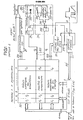
- the acquisition and averaging device consists essentially of a processing unit 1 and a sensor 2.
- the processing unit 1 is intended for calculating the digital values of the samples of the synthesized signal and will be detailed below.
- the sensor 2 is shown in Figure 1 and is intended to capture the characteristics of the error signal, called the difference signal, for each sample.
- the error signal e represents the difference between the synthesized signal calculated by the processing unit 1 and the noisy test signal to be analyzed T.
- the sensor 2 is organized around a random access memory 20 which is entirely under the control of the processing unit 1 when the sensor 2 does not receive the test signal T.
- the memory 20 is divided into three series cells Y, R and t which are each composed of a number of elementary cells equal to or greater than the integer number N of samples to be acquired.
- the first series Y 1 to Y N contains 12-bit words, for example, which represent the digital values of the samples.
- the second series of cells R 1 to R N contains 2-bit words Q 1 , Q 2 which indicate the result of the comparisons of the synthesized signal and the noisy test signal.
- the state of the first bit 0 1 of a word R indicates whether the module
- the state of the second bit Q 2 of a word R indicates the sign of the error signal e.
- the third series of cells t 1 to t N of the memory 20 contains 4-bit words, for example, which represent the digital values of the elementary steps of a sampling cycle.
- the results of the comparisons for each sample are mainly obtained by means of the component circuits 21 to 24.
- the digital sample Y n where n is an integer varying from 1 to N, is read after a duration equal to t n in the memory 20 which transmits it to a digital-analog converter 21, through a bus 200 with 12 wires.
- the analog sample S n is transmitted by the converter 21 to the reverse input (-) of a subtractor 22.
- the direct input (+) of the subtractor 22 receives the noisy periodic test signal T.
- This test signal can be, as already said, a standard signal such as the test signals inserted in lines No. 17 to 22 of a video signal.
- this test signal T has a period of 20 ms - equal to the image frame period - and to a first part having a duration t n of the order of 0.38 ms - that is to say of the order of 6 times the line period of 64 ⁇ s of the corresponding video signal -.
- the maximum time available to process the results of the comparisons is at most equal to the second part of the test signal period, ie of the order of 19.6 ms.
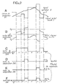
- the start of the test signal according to this example is the instant corresponding to the half-amplitude of the rising edge of the luminance bar of the test signal inserted in the line No. 17 of the video signal, as shown above the wire D in Fig. 1.
- An example of an error signal e is shown in Fig. 2B for a synthesized signal S and a noisy test signal T shown in FIG. 2A.
- the error signal is applied to the direct input (+) of a zero comparison circuit 23 and to direct (+) and inverse (-) inputs of a double threshold comparison circuit 24.
- the circuits 23 and 24 conventionally comprise operational amplifiers operating as a comparator. Circuit 23 includes a zero comparator 230, the output signal of which is shown in Fig. 2C and is transmitted to a flip-flop 231.
- Circuit 24 includes two comparators 240 and 241 which compare the signal ⁇ , respectively to the value of predetermined threshold S o and at its opposite value -S o .
- the output signals of the comparators 240 and 241 are shown in Figs. 2D and 2E.
- the circuit 24 also includes a flip-flop 242 whose input is connected to the outputs of the comparators 240 and 241 through an OR gate 243.
- the logic signal at the output of the OR gate 243 is shown in FIG. 2 F. It is high if
- > S o , which corresponds to the writing of a first bit Q 1 1 in the corresponding cell R n of the memory 20.
- the logic signal transmitted by the output of the comparator 23 (Fig.
- the two previous writes are performed at the end of the corresponding elementary step t n under the control of a clock signal 255 which is applied to the clock inputs of flip-flops 231 and 242.
- variable step sampling t 1 to t N is carried out by means of a variable step clock 25 and an address counter 26.
- the numerical values t 1 to t N are chosen beforehand as a function of the characteristics of the part of the test signal to be analyzed, which is at most equal to said first part of this signal.
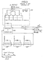
- the clock 25 comprises, according to a preferred example illustrated in FIG. 3, a loop of flip-flops 250 to 253 which is unlocked for the duration separating two signals which indicate the start and the end of the first part of the test signal to be acquired and which are applied to the inputs D and F of the clock 25 , respectively.
- the flip-flop loop comprises three monostable flip-flops 251 to 253 in series which are excited by a falling edge on their inputs in order to each produce a pulse having a duration of 1 ⁇ s for example. Three monostable scales are used instead of one for temperature stabilization purposes.
- the input of the first monostable lever 251 is connected to the output of lever 250 which is a locking lever.
- the output of the last flip-flop 253 constitutes the output 255 of the clock 25 which is connected to the input of the flip-flop 250 and also to the counting input of the address counter 26 and to the clock inputs of the flip-flops 231 and 242 (Fig. 1).
- the clock 25 also includes a JK 256 flip-flop, the inputs J and K are at "O", and an OR gate 257 whose inputs are connected to the output Q of the flip-flop 256 and to the input D of the clock 25 and whose output is connected to the input for controlling the locking of flip-flop 250.
- the reset input RA1 to "1" and the clock input H of flip-flop 256 are connected to inputs D and F.
- the locking control input of flip-flop 250 is at the high level, and consequently, the flip-flop 250 is unlocked, after a start pulse on input D until the next end pulse on input F. Then flip-flop 250 is locked until the next start pulse, that is to say the clock 25 is stopped so that the memory 20 is managed by the processing unit 1.
- a step decoder 258 receives, in parallel, the four bits of the words t 1 to t N which represent the digital values of the elementary clock steps and which are delivered on a bus 202 by the memory 20 on order of the address counter 26.
- the decoder 258 modifies the constant RC determining the width of the pulse of the latch flip-flop 250. It comprises, according to the example illustrated, four switches which each select or short-circuit a resistance as a function of the state of the bit of the associated rank in the received word t n .
- the duration between two samplings is constituted by a constant duration which is equal to the sum of the durations of 1 ⁇ s of the successive pulses supplied by the monostable flip-flops 251 to 253 and by the variable duration of the pulse supplied by the flip-flop 250.
- the rising edge of the start signal on wire D resets (reset) the address counter 26, which transmits through an access circuit 3, the first cell addresses Y 1 , R 1 , t 1 .
- the step decoder 258 of the clock 25 receives the word t 1 through the bus 202.
- the pulse at the output 255 of the clock 25 controls the flip-flops 231 and 242 and increments the address counter 26, which in turn transmits the addresses of cells Y 2 , R 2 and t 2 relating to the second sample to its output bus 260.
- These sequences of variable durations t 1 to t N continue until the address counter 26 has its count equal to N and emits the end of cycle signal on the wire F, which indicates the stopping of the sampling in sensor 2. This sampling will be resumed when a new start signal D appears corresponding to the next period of the test signal T.
- the address counter 26 reads cells Y and t and writes cells R.
- the address counter 26 is included in an internal logic circuit 27 having direct access to the memory 20.
- This logic circuit 27 is connected by a bus 260 to the memory 20 through the access circuit 3 and transmits, in addition addresses under the control of counter 26, certain data and commands such as instructions, depending on the state of counter 26, to allow proper readings and writes of the words contained in the memory 20.
- the words t representing the numerical values of the steps of the clock 25 are preprogrammed in the read-only memory of sequences of instructions of the processing unit 1 - as will be seen below - and are written in the corresponding cells of the memory 20 of the sensor 2 during the second part of each noisy signal period T.
- the processing unit 1 which makes it possible, during each period of the test signal T, after the end signal F, to calculate the new digital values Y of the samples in order to acquire by averaging the noise-free test signal.
- the processing unit 1 is preferably organized around a microprocessor 10, for example of the INTEL 8080 or MOTOROLA 6800 type.
- this microprocessor 10 is associated with a read only memory 11, that is to say - say addressing only in read mode, to a random access memory 12 serving as a buffer, and to an input-output interface 13.
- the circuits 11, 12, 13 are connected to the microprocessor 10 as well as to the sample memory 20 of the sensor 2 via the access circuit 3, through a unidirectional address bus 14, a bidirectional data bus 15 and a unidirectional control bus 16.
- the memory 11 contains, in addition to the various digital values t no clock, the sequences of instructions of the software of the microprocessor 10 which is specific to the calculation of the acquisition and the averaging of the samples.
- the buffer memory 12 stores certain iterative values A, B, C for each cycle of the program corresponding to a period of the test signal T.
- the input / output interface '13 makes it possible to transmit on a bus 17 to means of display, such as a printer or a display console (not shown), the results of the measurements carried out by digital calculation on the synthesized signal after the end of the acquisition procedure.
- the microprocessor 10 and the access circuit 3 receive on a wire 18 an envelope signal of the test signal T so that, during the useful period of the signal (between D and F), the access circuit 3 connects the memory 20 to the internal direct access logic unit 27 of the sensor 2, via the bus 260, in order to carry out the calculations of the characteristics of the error signal e for each sample and so that, for a duration less than or equal to the next period of time when the test signal T is absent, the buses 14, 15 and 16 are connected to the memory 20 and the microprocessor reads the results of the comparisons R 1 to R N and writes the new calculated values of the samples Y 1 at Y N.
- the calculation unit of FIG. 6 essentially comprises three comparison circuits 4, 5 and 6, a sample deviation selection circuit 7, an arithmetic and logic unit 8 and a logic circuit 9 for resetting the other circuits and transmitting the new value Y 'of the sample.
- Each of the comparison circuits 4, 5, 6 comprises a counter 40, 50, 60, a register 41, 51, 61 and a comparator 42, 52, 62 which compares, for each sample, the count of the counter and the content of the register.
- the comparators compare 8-bit words.
- the comparison circuit 4 also includes a flip-flop 43 whose output Q i is connected, through an AND gate 44, to the counting input of counter 40 and whose complementary output Q 1 is connected, through an AND gate 45, at the reset input (RESET) of the counter 40.
- a flip-flop 53 is also included in the comparison circuit 5 and at its output Q 2 which is connected to the counting input of the counter 50 through an AND gate 54.
- the other inputs of AND gates 44, 45, 54 as well as the counting input of the counter 60 are controlled by a so-called counting pulse IC which is transmitted on a wire 46 to initialize the start of the calculation of each sample.
- the comparison circuit 4 also includes an AND gate 47, the output of which is connected to the countdown input of the counter 40.
- One of the inputs of the AND gate 47 is connected to the output of the comparator 42, which is itself connected to one of the inputs of an OR gate 90 of the logic circuit 9 and to the selector control input 70 and 71 of the selection circuit 7.
- the other input of the AND gate 47 is connected to a wire 48 which transmits so-called ICA calculation pulses also to an input of an AND gate 91 of the logic circuit 9, the other input of which is connected to the output of the OR gate 90.
- the selector 70 has two input buses connected to two registers 72 and 73 which are respectively assigned to the fast and slow procedures, that is to say which include the increment or decrement rate raised to Y of the sample and the increment or decrement rate small ⁇ y of the sample.
- the selector 70 selects the content of one of the registers 72 and 73 according to the logic state a of the output of the comparator 42 to transmit it to a first buffer input register 80 of the arithmetic and logic unit 8.
- the selector 71 selects the output Q 2 of the flip-flop 53 or a first output 520 of the comparator 52 under the command of the logic state a of the output of comparator 42.
- the unit 8 comprises a second input buffer register 81 containing the preceding digital value Y n of the sample and an output buffer register 82 which receives the result Y ′ n of the addition or the subtraction.
- the logic circuit 9 comprises, in addition to the AND gate 91 and the OR gate 90, the other input of which is connected to the output of the comparator 62, also an inverter 92, an AND gate 93 and a register 94 in which the new value is loaded. of the sample contained in the output register 82 under the control of the output of the gate 93.
- the output of the gate 91 controls the resetting to zero (RESET) of the counters 50 and 60 and is connected to an input of the gate ET 93.
- the other input of the AND gate 93 is connected through the inverter 92 to a second output 521 of the comparator 52.
- the pulses IC and ICA as well as others necessary for the control of certain components of FIG. 6 are assumed to be transmitted by a control unit and a clock in relation to the instruction memory 11.
- a counting pulse IC is transmitted on the wire 46 which triggers the incrementation of a unit of the counter 60 and selectively as a function of the state of Q 1 and Q 2 the incrementation of a unit of the counters 40 and 50.
- > S o which puts the count of counter 40 at A ' n A n + 1
- ⁇ S o which puts through the gate AND 45 the count to zero of the counter 40: A ' n 0.
- the counter 40 therefore contains the number of successive periods where the module of the error signal ⁇ for the sample considered is greater than S o .
- the count of the counter 50 therefore contains the number of periods in which the corresponding sample of the error signal is positive.
- the comparator 42 compares the account A ' n of the counter 40 with a first predetermined number A o which is contained in the register 41. If the state a of the output of the comparator 42 is "1", this means that A' n ⁇ A o , that is to say that the sample of the synthesized signal S is very statistically different from that of the test signal T (
- the selector 70 transfers the content ⁇ y of the register 73 into the input register 80 of the unit 8 and the selector 71 transfers the state b of the first output 520 of the comparator 52 in the unit 8.
- the register 51 contains a number C 0/2 equal to half of a second predetermined even number C o contained in the register 61.
- the new value Y ′ n is transmitted to the memory 20 of the sensor 2 for the comparison during the following period of the test signal T. This comparison is followed by a new calculation of the value of the sample from the values of the results R ' n and parameters Y' n , A ' n , B' n and C ' n and so on for each sample according to the pre-described algorithm.
- the processing unit 1 with microprocessor 10 of FIG. 5 can be designed to manage several sensors 2 which operate on different test signals. These test signals can be, relatively to the television domain, the unfiltered test signal, the luminance waveform, the chrominance waveform detected in amplitude, the chrominance waveform detected in phase and waveform of the multisalve signal detected in amplitude.
Landscapes
- Physics & Mathematics (AREA)
- General Physics & Mathematics (AREA)
- Engineering & Computer Science (AREA)
- Health & Medical Sciences (AREA)
- Biomedical Technology (AREA)
- General Health & Medical Sciences (AREA)
- Multimedia (AREA)
- Signal Processing (AREA)
- Analogue/Digital Conversion (AREA)
- Measurement Of Current Or Voltage (AREA)
- Testing, Inspecting, Measuring Of Stereoscopic Televisions And Televisions (AREA)
- Noise Elimination (AREA)
Applications Claiming Priority (2)
| Application Number | Priority Date | Filing Date | Title |
|---|---|---|---|
| FR8005928A FR2478320A1 (fr) | 1980-03-17 | 1980-03-17 | Dispositif d'acquisition et de moyennage des echantillons d'un signal periodique bruite |
| FR8005928 | 1980-03-17 |
Publications (2)
| Publication Number | Publication Date |
|---|---|
| EP0036354A1 EP0036354A1 (fr) | 1981-09-23 |
| EP0036354B1 true EP0036354B1 (fr) | 1984-06-13 |
Family
ID=9239743
Family Applications (1)
| Application Number | Title | Priority Date | Filing Date |
|---|---|---|---|
| EP81400335A Expired EP0036354B1 (fr) | 1980-03-17 | 1981-03-04 | Dispositif d'acquisition et de moyennage des échantillons d'un signal périodique bruité |
Country Status (7)
| Country | Link |
|---|---|
| US (1) | US4352094A (en:Method) |
| EP (1) | EP0036354B1 (en:Method) |
| JP (1) | JPS5739680A (en:Method) |
| DE (1) | DE3164056D1 (en:Method) |
| ES (1) | ES8202998A1 (en:Method) |
| FR (1) | FR2478320A1 (en:Method) |
| GR (1) | GR74166B (en:Method) |
Families Citing this family (22)
| Publication number | Priority date | Publication date | Assignee | Title |
|---|---|---|---|---|
| FR2523791B1 (fr) * | 1982-03-19 | 1985-01-04 | Thomson Csf | Dispositif et appareil de test d'equipements electroniques notamment de television |
| US4493047A (en) * | 1982-04-05 | 1985-01-08 | The United States Of America As Represented By The Secretary Of The Navy | Real time data smoother and significant values selector |
| US4519025A (en) * | 1982-11-08 | 1985-05-21 | Gte Communication Systems Corporation | Sense point monitor circuit |
| FR2535854A1 (fr) * | 1982-11-10 | 1984-05-11 | Cit Alcatel | Procede et dispositif d'evaluation du niveau de bruit sur une voie telephonique |
| US4596024A (en) * | 1983-05-23 | 1986-06-17 | At&T Bell Laboratories | Data detector using probabalistic information in received signals |
| JPS6011119A (ja) * | 1983-06-30 | 1985-01-21 | Shimadzu Corp | 電子天びん |
| CA1306504C (en) * | 1986-03-05 | 1992-08-18 | Nec Corporation | Noise detection by sampling digital baseband signal at eye openings |
| US4868885A (en) * | 1986-05-05 | 1989-09-19 | General Electric Company | Apparatus and method for high-speed determination of received RF signal strength indicator |
| US4825379A (en) * | 1986-08-29 | 1989-04-25 | Tektronix, Inc. | Method and apparatus for processing waveform records for jitter elimination prior to averaging in determining signal to noise ratio |
| US4769760A (en) * | 1987-03-13 | 1988-09-06 | Cherne Medical, Inc. | Terrain biased dynamic multiple threshold synchronization method and apparatus |
| US5424961A (en) * | 1988-03-04 | 1995-06-13 | Brust; Hans-Detlef | Process and system for measuring the temporal course of a periodic signal having high time resolution according to a "Boxcar-like" process |
| ATE92639T1 (de) * | 1988-06-13 | 1993-08-15 | Siemens Ag | Verfahren zur stoerunterdrueckung bei ultraschall- abstandsmessungen. |
| US5119321A (en) * | 1990-05-14 | 1992-06-02 | Harris Corporation | Adaptive threshold suppression of impulse noise |
| FR2670016A1 (fr) * | 1990-11-30 | 1992-06-05 | Sqchlumberger Ind | Dispositif de mesure de bruit. |
| US5465227A (en) * | 1993-10-14 | 1995-11-07 | Simmonds Precision Products, Inc. | Real time auto-correlation filter method and apparatus |
| DE19944985B4 (de) * | 1999-09-20 | 2005-04-28 | Siemens Ag | Messverfahren zur Strommessung mit Rauschunterdrückung |
| DE10243564B4 (de) * | 2002-09-19 | 2006-11-30 | Siemens Ag | Schaltungsanordnung zur Mittelwertbildung |
| US20040119455A1 (en) * | 2002-12-18 | 2004-06-24 | Sunter Stephen K. | Method for testing parameters of high speed data signals |
| US8031169B2 (en) * | 2003-12-17 | 2011-10-04 | Riip, Inc. | Automated system and method for high-frequency signal attenuation compensation |
| JP6061675B2 (ja) * | 2012-12-28 | 2017-01-18 | 株式会社アドバンテスト | 測定装置および電子デバイス |
| US9261026B2 (en) * | 2013-06-27 | 2016-02-16 | Pratt & Whitney Canada Corp. | System and method for conditioning noisy signals |
| US11695283B2 (en) * | 2018-05-11 | 2023-07-04 | Texas Instruments Incorporated | Shoot-through current limiting circuit |
Citations (2)
| Publication number | Priority date | Publication date | Assignee | Title |
|---|---|---|---|---|
| FR2031132A5 (en:Method) * | 1969-02-04 | 1970-11-13 | Rai Radiotelevisione Italiana | |
| FR2290114A1 (fr) * | 1974-11-01 | 1976-05-28 | Indep Broadcasting Authority | Controle de qualite de signaux de television par addition de signaux de test d'insertion |
Family Cites Families (2)
| Publication number | Priority date | Publication date | Assignee | Title |
|---|---|---|---|---|
| US3441720A (en) * | 1964-12-10 | 1969-04-29 | United Aircraft Corp | Apparatus for providing a digital average of a plurality of analogue input samples |
| DE2700772A1 (de) * | 1977-01-10 | 1978-07-13 | Bosch Gmbh Robert | Verfahren zur feststellung des rauschanteils eines elektrischen signals |
-
1980
- 1980-03-17 FR FR8005928A patent/FR2478320A1/fr active Granted
-
1981
- 1981-03-04 EP EP81400335A patent/EP0036354B1/fr not_active Expired
- 1981-03-04 DE DE8181400335T patent/DE3164056D1/de not_active Expired
- 1981-03-11 US US06/242,623 patent/US4352094A/en not_active Expired - Lifetime
- 1981-03-16 GR GR64400A patent/GR74166B/el unknown
- 1981-03-17 JP JP56037346A patent/JPS5739680A/ja active Pending
- 1981-03-17 ES ES500436A patent/ES8202998A1/es not_active Expired
Patent Citations (2)
| Publication number | Priority date | Publication date | Assignee | Title |
|---|---|---|---|---|
| FR2031132A5 (en:Method) * | 1969-02-04 | 1970-11-13 | Rai Radiotelevisione Italiana | |
| FR2290114A1 (fr) * | 1974-11-01 | 1976-05-28 | Indep Broadcasting Authority | Controle de qualite de signaux de television par addition de signaux de test d'insertion |
Also Published As
| Publication number | Publication date |
|---|---|
| ES500436A0 (es) | 1982-02-01 |
| DE3164056D1 (en) | 1984-07-19 |
| JPS5739680A (en) | 1982-03-04 |
| FR2478320B1 (en:Method) | 1983-07-18 |
| GR74166B (en:Method) | 1984-06-07 |
| ES8202998A1 (es) | 1982-02-01 |
| US4352094A (en) | 1982-09-28 |
| FR2478320A1 (fr) | 1981-09-18 |
| EP0036354A1 (fr) | 1981-09-23 |
Similar Documents
| Publication | Publication Date | Title |
|---|---|---|
| EP0036354B1 (fr) | Dispositif d'acquisition et de moyennage des échantillons d'un signal périodique bruité | |
| US4495586A (en) | Waveform acquisition apparatus and method | |
| FR2462760A1 (fr) | Systeme de memoire pour une forme d'onde electromagnetique | |
| EP1080432B1 (fr) | Systeme d'acquisition de donnees comprenant des moyens d'analyse et de stockage en temps reel | |
| KR100272626B1 (ko) | 스큐우 타이밍 에러 측정용 장치 | |
| EP0089873A1 (fr) | Dispositif et appareil de test d'équipements électroniques, notamment de télévision | |
| FR2519147A1 (fr) | Analyseur logique | |
| EP0071506B1 (fr) | Procédé et dispositif numérique de correction d'erreur de phase d'un signal échantillonné et son application à la correction de signaux de télévision | |
| FR2532504A1 (fr) | Dispositif pour ameliorer le rapport signal-bruit du canal de couleur dans un recepteur de television numerique | |
| FR2464479A1 (fr) | Oscilloscope numerique a reduction du vacillement du a l'incertitude des echantillons | |
| FR2665541A1 (fr) | Appareil de manipulation de valeurs numeriques, ainsi que son procede de mise en óoeuvre, notamment en vue de la production d'un affichage graphique. | |
| JP2574038B2 (ja) | 同期サンプリング・システムおよび方法 | |
| FR2610773A1 (fr) | Systeme de synchronisation sur un signal semi-numerique | |
| EP0674302B1 (fr) | Procédé de reconnaissence de standard vidéo, et circuit mettant en oeuvre ce procédé | |
| FR2548490A1 (fr) | Circuit programmable de transformation serie-parallele d'un signal numerique, et son application a un recepteur de signaux video numeriques | |
| US5008940A (en) | Method and apparatus for analyzing and reconstructing an analog signal | |
| EP0462654A1 (fr) | Procédé de réglage d'un décodeur à seuil pour un signal à plusieurs niveaux et récepteur de télévision muni d'un tel décodeur | |
| FR2510330A1 (fr) | Procede et dispositif pour l'echantillonnage d'un signal sinusoidal de frequence determinee par un signal de frequence multiple de cette frequence determinee | |
| EP3140910B1 (fr) | Convertisseur analogique-numérique à rampe apte à fournir directement une moyenne de deux signaux | |
| FR2562290A1 (fr) | Dispositif de traitement de signaux electro-oculographiques | |
| TN | Introduction to digital signal processing | |
| JPH01284069A (ja) | 画像入力装置 | |
| FR2473825A1 (fr) | Appareil pour controler des transmissions de donnees numeriques, et procede a cet effet | |
| FR2501941A1 (fr) | Procede et dispositif d'accentuation des traits d'une image en noir et blanc reproduite a partir d'une transcription numerique | |
| EP0336336A1 (fr) | Circuit de mesure de taux d'erreurs pour équipement de transmission numérique synchrone |
Legal Events
| Date | Code | Title | Description |
|---|---|---|---|
| PUAI | Public reference made under article 153(3) epc to a published international application that has entered the european phase |
Free format text: ORIGINAL CODE: 0009012 |
|
| AK | Designated contracting states |
Designated state(s): BE CH DE GB IT NL SE |
|
| 17P | Request for examination filed |
Effective date: 19811013 |
|
| ITF | It: translation for a ep patent filed | ||
| GRAA | (expected) grant |
Free format text: ORIGINAL CODE: 0009210 |
|
| AK | Designated contracting states |
Designated state(s): BE CH DE GB IT LI NL SE |
|
| REF | Corresponds to: |
Ref document number: 3164056 Country of ref document: DE Date of ref document: 19840719 |
|
| PLBE | No opposition filed within time limit |
Free format text: ORIGINAL CODE: 0009261 |
|
| STAA | Information on the status of an ep patent application or granted ep patent |
Free format text: STATUS: NO OPPOSITION FILED WITHIN TIME LIMIT |
|
| 26N | No opposition filed | ||
| ITTA | It: last paid annual fee | ||
| EAL | Se: european patent in force in sweden |
Ref document number: 81400335.6 |
|
| PGFP | Annual fee paid to national office [announced via postgrant information from national office to epo] |
Ref country code: NL Payment date: 19960111 Year of fee payment: 16 |
|
| PGFP | Annual fee paid to national office [announced via postgrant information from national office to epo] |
Ref country code: CH Payment date: 19960212 Year of fee payment: 16 |
|
| PGFP | Annual fee paid to national office [announced via postgrant information from national office to epo] |
Ref country code: GB Payment date: 19960219 Year of fee payment: 16 Ref country code: DE Payment date: 19960219 Year of fee payment: 16 |
|
| PGFP | Annual fee paid to national office [announced via postgrant information from national office to epo] |
Ref country code: BE Payment date: 19960305 Year of fee payment: 16 |
|
| PGFP | Annual fee paid to national office [announced via postgrant information from national office to epo] |
Ref country code: SE Payment date: 19960320 Year of fee payment: 16 |
|
| PG25 | Lapsed in a contracting state [announced via postgrant information from national office to epo] |
Ref country code: GB Effective date: 19970304 |
|
| PG25 | Lapsed in a contracting state [announced via postgrant information from national office to epo] |
Ref country code: SE Effective date: 19970305 |
|
| PG25 | Lapsed in a contracting state [announced via postgrant information from national office to epo] |
Ref country code: LI Effective date: 19970331 Ref country code: CH Effective date: 19970331 Ref country code: BE Effective date: 19970331 |
|
| BERE | Be: lapsed |
Owner name: ETS PUBLIC TELEDIFFUSION DE FRANCE Effective date: 19970331 |
|
| PG25 | Lapsed in a contracting state [announced via postgrant information from national office to epo] |
Ref country code: NL Effective date: 19971001 |
|
| GBPC | Gb: european patent ceased through non-payment of renewal fee |
Effective date: 19970304 |
|
| REG | Reference to a national code |
Ref country code: CH Ref legal event code: PL |
|
| NLV4 | Nl: lapsed or anulled due to non-payment of the annual fee |
Effective date: 19971001 |
|
| EUG | Se: european patent has lapsed |
Ref document number: 81400335.6 |
|
| PG25 | Lapsed in a contracting state [announced via postgrant information from national office to epo] |
Ref country code: DE Free format text: LAPSE BECAUSE OF NON-PAYMENT OF DUE FEES Effective date: 19980203 |