EP0033162A2 - Digitaler Tonfrequenz-Wecker - Google Patents
Digitaler Tonfrequenz-Wecker Download PDFInfo
- Publication number
- EP0033162A2 EP0033162A2 EP81100623A EP81100623A EP0033162A2 EP 0033162 A2 EP0033162 A2 EP 0033162A2 EP 81100623 A EP81100623 A EP 81100623A EP 81100623 A EP81100623 A EP 81100623A EP 0033162 A2 EP0033162 A2 EP 0033162A2
- Authority
- EP
- European Patent Office
- Prior art keywords
- signal
- frequency
- wire
- call
- apt
- Prior art date
- Legal status (The legal status is an assumption and is not a legal conclusion. Google has not performed a legal analysis and makes no representation as to the accuracy of the status listed.)
- Granted
Links
- 230000005284 excitation Effects 0.000 claims 1
- 239000013256 coordination polymer Substances 0.000 description 8
- 230000000694 effects Effects 0.000 description 7
- 239000002775 capsule Substances 0.000 description 4
- 238000012986 modification Methods 0.000 description 3
- 230000004048 modification Effects 0.000 description 3
- 238000010586 diagram Methods 0.000 description 2
- 238000010521 absorption reaction Methods 0.000 description 1
- 230000008030 elimination Effects 0.000 description 1
- 238000003379 elimination reaction Methods 0.000 description 1
- 238000003780 insertion Methods 0.000 description 1
- 230000037431 insertion Effects 0.000 description 1
- 238000004519 manufacturing process Methods 0.000 description 1
Images

Classifications
-
- H—ELECTRICITY
- H04—ELECTRIC COMMUNICATION TECHNIQUE
- H04M—TELEPHONIC COMMUNICATION
- H04M19/00—Current supply arrangements for telephone systems
- H04M19/02—Current supply arrangements for telephone systems providing ringing current or supervisory tones, e.g. dialling tone or busy tone
- H04M19/04—Current supply arrangements for telephone systems providing ringing current or supervisory tones, e.g. dialling tone or busy tone the ringing-current being generated at the substations
Definitions
- This invention relates to tone ringers for use in telephone sets and more particularly it concerns a digital telephone ringer able to receive call signals coming both from conventional electro mechanical exchanges and from up-to-date electronic exchanges.
- the telephone service is controlled either by conventional electro mechanical or electronic exchanges.
- As known said signals are able to directly excite a conventional tone ringer of electro mechanical type.
- Electronic exchanges generally emit a voice-band tone ringer whose frequency range is 400 to 500 Hz and whose voltage level is much lower (of the order of a few volts) and thus cannot directly excite electro-mechanical tone-ringer. Consequently, in telephone sets connected with electronic exchanges a suitable electronic tone ringer is provided. However, electronic tone ringers cannot be directly excited by the call signals of electro mechanical exchanges.
- control of the call signal of the electromechanical type is unsatisfactory because only an amplitude check and an insufficient duration check are made that cannot filter the noises of 50Hz induced by the electrical networks as well as those due to the dialling operated by telephone sets in parallel.
- a further disadvantage of the tone ringer described in said Italian Patent Application is that it can be activated also by the voice during a call, because no protection means able to switch off during the call the devices designed to detect the call signals coming from exchanges I of the electronic type are provided.
- an analog ringer entails insufficient protection against noises; high fabrication costs as said ringer is difficult to make by integrated technology; high power dissipation in the absence of a call signal.
- tone ringer of the digital type whose operation requires no polarity inversion on the subscriber's loop, but is protected against accidental polaritys inversions; it is directly fed from the loop and is designed thus as to limit current absorption from the line so as to allow the insertion of at least five parallel tone ringers; that, by recognizing the amplitude, the frequency, and the duration of the call signal is protected against noises present along the line; that can produce a sound having equal characteristics independently of the call signal; that being of the digital type is easy to integrate and therefore cheap and reliable; that has independent circuits for the operation both with signals of the conventional type and with signals coming from electronic exchanges so that circuits judged unnecessary can be cut-off.
- Another characteristic of the considered tone ringer is that by easy modifications can be made apt to recognize call frequencies also different from the abovementioned ones.
- An object of the present invention is to provide a tone ringer of digital kind which is apt to energize an electro acoustic transducer on the basis of a call signal coming along the line from a telephone exchange, that identifies the call signal by operating a series of amplitude, frequency and duration checks on said call signal and in which independent circuits that can be mutually excluded are provided, designed to make such identification on the call signals coming both from telephone electronic exchanges and from electromechanical telephone exchanges.
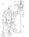
- Reference GP in Fig. 1 denotes a circuit protecting against polarity inversion composed for instance of a diode bridge, able to protect the remaining circuit from accidental polarity inversion that might occur on the subscriber's loop denoted by L; GP receives the call signal from line L and emits at the output on wire 1 a signal whose polarity never changes.
- Reference II denotes an input interface able to match the voltage levels of the signals coming from line L and present on wire 1 to levels compatible with the circuits placed after; afterwards besides II emits at the output a pulsive signal of the same frequency as the signal received at the input.
- Reference IN denotes a usual signal detector, able to emit at the output on wire 3 an enabling signal when at its input, connected to II through wire 2, any signal may be present.
- Reference RS denotes a usual detector of threshold signal, able to emit at the output on wire 4 a logic signal where at its input, connected to wire 1, a signal is present of amplitude exceeding a pre- determined threshold.
- Said threshold is dimensioned in accordance with the minimum acceptable value of the call signal coming from telephone exchanges of electromechanical type.
- References Al and A2 denote two conventional power regulators of the series type able to stabilize the voltage, present on wire 1, coming from line L, so as to match it to the voltages needed for feeding some blocks of the ringing circuit.
- A provides at the output a d. c. voltage supply apt to driving a conventional output interface IO, that in turn is apt to driving an electroacoustic transducer, for instance a telephone capsule CP used to reproduce the ringing tone.
- Interface IO receives, as it will be seen, from wire 7 the signal that is to be reproduced by capsule CP.
- A2 receives from A1, by means of wire 5, a dc- voltage already stabilized and emits at the output on wire 6 a dc- voltage, reduced with respect to the one oi the input, just when the input voltage, is beyond a pre-determined value; otherwise it produces at the output a voltage level near zero.
- This behaviour of A2 is obtained by simply introducing a threshold system, for instance a zener diode, at its input.
- Reference CR denotes a circuit able to effect the recognition of the call signal; CR, that will be examined in details in connection with Fig. 2, receives: the supply from A2 by means of wire 6; the signal to be recognized from II by means of wire 2; a signal enabling to the operation arriving from IN via wire 3, and an enabling signal, arriving from RS via wire 4, that will be used, as seen hereinafter, to transfer inside circuit CR the signal indicating the possible occurrence of the recognition of a call signal.
- CR emits at the output on wire 7 towards IO the ringing signal that must be reproduced by CP.
- Reference G in Fig. 2 denotes a circuit of the known type apt to divide by two the frequency of the pulsive signal it receives at the input from wire 2, so that it emits at the output on wire 8 a signal that with respect to that present on wire 2 has half frequency and then duty cycle equal to 50%.
- Reference OS denotes a conventional oscillator apt to generate on wire 9 a pulsive signal of frequency fb that serves, as will be seen hereinafter, for the measure of the frequency of the call signal present on wire 8.
- Reference PI denotes a usual AND gate, apt to receive at the two inpuls the signals present on wires 8 and 9 and to emit at the output on wire 10 the logic AND of the two signals, basically consisting of a signal of frequency fb for as long as the pulsive signal, present on wire 8, is at logic value "I".
- Reference CL denotes a usual delay circuit apt to emit at the output on wire 11 a reset signal after a pre-determined time interval since the level of the logic signal that receives at the input on wire 8 has reached logic level "0".
- Reference CM denotes a usual comiter able to count the number of signal periods at frequency fb received by PI via wire 10; CM that is reset by the signal it receives from CL via wire 11, emits at the output on connection 12 the binary signal corresponding to the effected counting.
- Reference LD denotes a logic network able to recognize, upon receiving the enabling (signal) from wire 3, the binary number received from CM through connection 12. This recognition is repeated whenever the signal present on wire 8 is at logic level "1", said condition is detected by LD through the signal present on wire 11 at the output of CL.
- LD basically consists of two combinatory logics RF1, RF2, of two gates of AND type P4, P5,and of an inverter I.
- Both combinatory logics RFI, RF2 receive at the input from connection 12 the binary signal emitted by CM, corresponding to the value of the frequency of the call signal.
- RF is provided for the recognition of the frequency of call signals of the conventional type; RF2 for the recognition of the signals of the electronic type.
- RF1 effects the recognition and emits at the output a pulse towards gate P4, while RF2 remains in rest condition (i. e. is not activated ). If said binary number present on connection 12 corresponds, on the contrary, to a call of the electronic type, RF2 effects its recognition by emitting a pulse at the input towards gate P5, while RF1 remains in rest condition.
- RF1 and RF2 are enabled to effect the recognition by the signal present on wire 3, that as mentioned is present only when a signal is present on line L (Fig. 1); moreover RF1 and RF2 (Fig. 2) repeat the recognition operation whenever the signal present on wire 8 is at logic level "1" what is possible because RF1 and RF2 are rearrangedforthe recognition bythe"reset signal” coming from wire 11 that, as previously seen, depends on the logic level present on wire 8.
- Gates P4 and P5 are enabled by the signal present on wire 4 to the transfer, on wires 13 and 14 respectively, of the signal that may be present on the outputs of RF] and RF2. More particularly if the signal present on wire 4 is at logic level "0" gate P4 is inhibited while gate P5 is enabled due to the operation of inverter I.
- Reference C1 denotes a usual counter of the presettable type, able to receive from wire 13 the pulses coming from LD relative to a call of an electromechanical kind, to count on the basis of the enabling signal received from wire 8, a determined number of said pulses fixed during the presetting step and to emit at the output on wire 15 a signal of occurred call recognition of electromechanical type; the signal on wire 15 lasts for as long as the signal received by C1 from wire 16 is at logic level "1"
- Reference C2 denotes a conventional counter equal to C1, but preset on a different basis, that carries out the same functions as to what concerns the pulses coming, via wire 14, from LD concerning a call of electronic type.
- C2 emits at the output on wire 17 a signal of occurred recognition of a signal of the electronic type, whose duration, analogously to what takes place for Cl, depends on logic level "1" of the signal it receives from wire 16.
- Reference P2 denotes a conventional logic gate of the OR type, apt to transfer at the output on wire 18 either the signals of occurred recognition that exclude one another, received at the input from wires 15 and 17.
- Reference GSC denotes a circuit, whose structure will be examined hereinafter, apt to generate on wire 7 the actual ringing tone signal to be sent to IO (Fig. 1) and reproduced by capsule CP.
- GSC receives from wire 9 the signal at frequency fb, generated by OS; from wire 18 the enable signal designed to emit the ringing signal, on wire 7. GSC emits on wire 16 a signal that is to interrupt, in accordance with suitable criteria to be examined hereinafter the generation of the ringing signal.
- GSC is also designed to adapt to the specifications the shape and the duration of the ringing tone.
- the ringing signal frequency is of 1KHz (or 500 Hz) modulated at 20 Hz for the duration of one second.
- circuit GSC has been implemented for instance as in Fig. 2 by blocks DV1, DV2, DV3 and P3.
- Reference DV1 denotes a frequency divider able to divide frequency fb, received from wire 9, so as to obtain the frequency of 1KHz (500 Hz) at the output on wire 19 as long as it receives the enabling signal of wire 18.
- Reference DV2 denotes a frequency divider, analogous to DV1, apt to convert the signal at 1 KHz (500-Hz) it receives from DV1 via wire 19, into a signal at 20 Hz that it emits at the output on wire 20 for the whole time during which it receives the enabling signal from wire 18.
- Reference DV3 denotes a frequency divider, analogous to DV1 and DV2, able to receive the signal at 20 Hz from DV2 via wire 20 and to amit at the output on wire 16 a signal at logic level "0" just a secondafter the enabling signal, already examined, appears on wire 18.
- Reference P3 denotes a usual AND gate, able to supply at the output on wire 7 the logic AND of the two signals received at the input from wire 19 and 20, that is a signal consisting of subsequent trains of pulses at 1 KHz of the duration of 25 milliseconds.
- circuit GSC must have a different structure apt to the purpose; in any case its practical embodiment is not a problem to the person skilled in the art.
- the call signal that may be present on line L (Fig. 1), consists, as well known, in the superimposition of the alternating voltage of the proper call signal upon the dc supply voltage, coming from the exchange.
- GP (Fig. 1) transfers the call signal, it receives from L, onto wire 1, so that the polarity on wire 1 may remain unchanged, for instance positive with respect to ground potential.
- the voltage present on wire 1 is stabilized by regulator Al and converted into d. c. voltage emitted on wire 5 apt to drive, by means of interface IO, telephone capsule CP.
- Said d. c. voltage, present on wire 5 is reduced by A2 so as to obtain on wire 6 the d.c. voltage, necessary to supply blocks II and CR, only when the d. c. voltage present on wire 5 is higherthanapre- determined value (for instance: higher than 20 V).
- A2 generates at the output on wire 6 a voltage level near zero so as to inhibit the operation of blocks II and CR.
- circuit GSC that has the only task of producing thewaveform required for the ringing signal to send, through wires 7 and IO, to CP, once the logic circuits prior to GSC have detected the presence of the call signal on line L and have identified the signal type.
- GSC once it has been activated by the enable signal coming from P2 through wire 18, emits at the output on wire 16 towards C and C2 a signal that is generally at logic level “1” and goes into logic level “0” for a short time period, exactly with the delay of one second from the instant at which GSC has received from P2 the enable signal; logic "0" emitted on wire 16 resets counters Cl and C2.
- circuit of Fig. 1 is generally designed to recognize a possible call signal of the electronic type.
- G (Fig. 2) emits at the output on wire 8 a pulsive signal having frequency equal to half the signal present on wire 1, and then on wire 2; whenever the logic level on wire 8 is at logic value "1", Cl and C2 are enabled to the counting and Pl is enabled to transfer at the output on wire 10 towards CM the frequency signal fb it receives from OS via wire 9.
- CM counts the pulses of fb and emits the result of this counting with binary coding on connection 12 towards LD, that decodes the meaning.
- LD emits on wire 14 towards C2 a pulse every time the level of the signal present on wire 8 is at logic level "I".
- Said ringing signal will last a second, because after that time the reset signal for C2 will be emitted from GSC on wire 16.
- Said signal is recognized by RS, as it has an amplitude sufficiently higher than the threshold fixed for it; as a consequence RS sends a logic "I" to LD (Fig. 2), via wire 4, so as to disable gate P5 and therefore the output connected to wire 14 and so as to enable gate P4 and therefore the output connected to wire 13.
- the most frequent and dangerous is that at 50 Hz induced by the electrical supply netwo rk.
- LD would refuse said signal at 50 Hz; but that generally is impossible because in a number of telephone networks, as for instance the Italian one, the frequency at 50 Hz is utilized as call signal in a number of exchanges.
- the actual call signal at 50 Hz is different from the noise at the same frequency for two main reasons: the amplitude, that for noises can hardly exceed the value of 60 V peak-to peak, equal to that of the threshold provided in RS; the duration, that in case )f an actual call signal is of the order of one second while a noise at a frequency of 50 Hz cannot easily maintain the amplitude at a value exceeding 60 volts for nearly one second.
- the ringing circuit object of the invention filters also the noises deriving from other auxiliary telephone sets, connected in parallel with the calling one, as, for instance, the noises due to the telephone dial and to off-hook.
- noises generally correspond to a sequence of pulses at 10 Hz and as such they are filtered by the frequency identifiers RF1, RF2 of LD.
- a variation of the just described tone ringer consists in providing the frequency divider DV3 (Fig. 2) contained in GSC with a simple counter modulo 2 so as to allow DV3 to discriminate the first ringing pulse, consequent to the apparence of signal on wire 8, with respect to the remaining ringing pulses.
Landscapes
- Engineering & Computer Science (AREA)
- Signal Processing (AREA)
- Telephonic Communication Services (AREA)
- Devices For Supply Of Signal Current (AREA)
- Monitoring And Testing Of Exchanges (AREA)
Applications Claiming Priority (2)
| Application Number | Priority Date | Filing Date | Title |
|---|---|---|---|
| IT67119/80A IT1127993B (it) | 1980-01-29 | 1980-01-29 | Suoneria telefonica di tipo digitale |
| IT6711980 | 1980-01-29 |
Publications (3)
| Publication Number | Publication Date |
|---|---|
| EP0033162A2 true EP0033162A2 (de) | 1981-08-05 |
| EP0033162A3 EP0033162A3 (en) | 1981-08-19 |
| EP0033162B1 EP0033162B1 (de) | 1984-10-17 |
Family
ID=11299733
Family Applications (1)
| Application Number | Title | Priority Date | Filing Date |
|---|---|---|---|
| EP81100623A Expired EP0033162B1 (de) | 1980-01-29 | 1981-01-28 | Digitaler Tonfrequenz-Wecker |
Country Status (10)
| Country | Link |
|---|---|
| US (1) | US4365116A (de) |
| EP (1) | EP0033162B1 (de) |
| JP (1) | JPS56114467A (de) |
| BR (1) | BR8100379A (de) |
| CA (1) | CA1162337A (de) |
| DE (1) | DE3166657D1 (de) |
| DK (1) | DK154598B (de) |
| ES (1) | ES8202219A1 (de) |
| IT (1) | IT1127993B (de) |
| MX (1) | MX149525A (de) |
Cited By (1)
| Publication number | Priority date | Publication date | Assignee | Title |
|---|---|---|---|---|
| EP0135538A4 (de) * | 1983-02-28 | 1987-12-08 | American Telephone & Telegraph | Elektronische wählsignale. |
Families Citing this family (4)
| Publication number | Priority date | Publication date | Assignee | Title |
|---|---|---|---|---|
| JP2535532Y2 (ja) * | 1989-02-10 | 1997-05-14 | ローム 株式会社 | マイコンダイアラ |
| US6775531B1 (en) | 1994-07-21 | 2004-08-10 | Interdigital Technology Corporation | Subscriber terminal temperature regulation |
| US6243399B1 (en) * | 1994-07-21 | 2001-06-05 | Interdigital Technology Corporation | Ring signal generator |
| US5610978A (en) * | 1994-12-30 | 1997-03-11 | Mitel Corporation | Ring discriminator |
Family Cites Families (7)
| Publication number | Priority date | Publication date | Assignee | Title |
|---|---|---|---|---|
| NL112535C (de) * | 1956-06-07 | |||
| US3508012A (en) * | 1967-11-24 | 1970-04-21 | Bell Telephone Labor Inc | Compatible tone ringer |
| US3603740A (en) * | 1969-08-18 | 1971-09-07 | Northern Electric Co | Method and means for ringing a telephone subset |
| US3808379A (en) * | 1972-05-30 | 1974-04-30 | Gte Automatic Electric Lab Inc | Telephone tone ringer |
| DE2520532B2 (de) * | 1975-05-07 | 1978-09-21 | Siemens Ag, 1000 Berlin Und 8000 Muenchen | Schaltungsanordnung für eine Ruftoneinrichtung für Fernmelde-, insbesondere Fernsprechanlagen |
| IT1143632B (it) * | 1977-01-24 | 1986-10-22 | Sits Soc It Telecom Siemens | Circuito rivelatore di chiamata acustica,specialmente per apparecchi telefonici |
| IT1083388B (it) * | 1977-06-20 | 1985-05-21 | Cselt Centro Studi Lab Telecom | Suoneria elettronica per apparecchi telefonici |
-
1980
- 1980-01-29 IT IT67119/80A patent/IT1127993B/it active
-
1981
- 1981-01-14 MX MX185562A patent/MX149525A/es unknown
- 1981-01-16 DK DK019981AA patent/DK154598B/da unknown
- 1981-01-21 ES ES498704A patent/ES8202219A1/es not_active Expired
- 1981-01-23 BR BR8100379A patent/BR8100379A/pt unknown
- 1981-01-23 CA CA000369184A patent/CA1162337A/en not_active Expired
- 1981-01-26 JP JP914081A patent/JPS56114467A/ja active Pending
- 1981-01-28 EP EP81100623A patent/EP0033162B1/de not_active Expired
- 1981-01-28 US US06/229,174 patent/US4365116A/en not_active Expired - Fee Related
- 1981-01-28 DE DE8181100623T patent/DE3166657D1/de not_active Expired
Cited By (1)
| Publication number | Priority date | Publication date | Assignee | Title |
|---|---|---|---|---|
| EP0135538A4 (de) * | 1983-02-28 | 1987-12-08 | American Telephone & Telegraph | Elektronische wählsignale. |
Also Published As
| Publication number | Publication date |
|---|---|
| ES498704A0 (es) | 1982-01-01 |
| IT8067119A0 (it) | 1980-01-29 |
| DK19981A (da) | 1981-07-30 |
| DE3166657D1 (en) | 1984-11-22 |
| BR8100379A (pt) | 1981-08-11 |
| EP0033162A3 (en) | 1981-08-19 |
| ES8202219A1 (es) | 1982-01-01 |
| JPS56114467A (en) | 1981-09-09 |
| MX149525A (es) | 1983-11-18 |
| IT1127993B (it) | 1986-05-28 |
| US4365116A (en) | 1982-12-21 |
| DK154598B (da) | 1988-11-28 |
| EP0033162B1 (de) | 1984-10-17 |
| CA1162337A (en) | 1984-02-14 |
Similar Documents
| Publication | Publication Date | Title |
|---|---|---|
| US5327493A (en) | Device for detecting tones on telephone lines | |
| US4146754A (en) | Telephone signalling method and apparatus | |
| US4066848A (en) | Telephone ring detector circuit | |
| US3867585A (en) | Electronic tone ringer | |
| US4508937A (en) | Method and circuitry for encoding telephone ringing signals | |
| EP0143481B1 (de) | Zweitonmehrfrequenz-Fernsprecher mit Vielfachgebrauch der Logika des digitalen Frequenz-Generators | |
| US20020080924A1 (en) | Telephone line monitoring and alarm apparatus | |
| EP0033162B1 (de) | Digitaler Tonfrequenz-Wecker | |
| GB2158677A (en) | Line powered flasher circuit for providing visual indication of telephone ringing signal | |
| US4367376A (en) | Electronic telephone ringer including anti-bell tap provisions | |
| US3808379A (en) | Telephone tone ringer | |
| Meacham et al. | Tone Ringing and Pushbutton Calling: Two Integrated Exploratory Developments | |
| US3965307A (en) | Electronic tone ringer | |
| US4491691A (en) | Electronic tone ringer | |
| US4112261A (en) | Key telephone system and method | |
| US3466403A (en) | Telephone calling tone circuit | |
| US3420963A (en) | Communication system line circuit particularly for key telephone systems | |
| US3936617A (en) | Code-controlled ringer attachment for telephones | |
| EP0165516B1 (de) | Rufsignalübertragungsanordnung | |
| US4152549A (en) | Suppressor of spurious ringing currents for telephone apparatus | |
| US3746795A (en) | Long line adapter circuit usable with increased power supply | |
| US4154989A (en) | Call-signal receiver for station of telecommunication system | |
| EP0454262A1 (de) | Elektronische Schaltung zur Meldung und/oder Verhinderung einer unbefugten Benutzung einer Fernsprechteilnehmerleitung | |
| US4140884A (en) | Electronic tone ringer | |
| US4748659A (en) | Calling signal transmission apparatus |
Legal Events
| Date | Code | Title | Description |
|---|---|---|---|
| PUAI | Public reference made under article 153(3) epc to a published international application that has entered the european phase |
Free format text: ORIGINAL CODE: 0009012 |
|
| PUAL | Search report despatched |
Free format text: ORIGINAL CODE: 0009013 |
|
| AK | Designated contracting states |
Designated state(s): BE CH DE FR GB LI NL SE |
|
| AK | Designated contracting states |
Designated state(s): BE CH DE FR GB LI NL SE |
|
| 17P | Request for examination filed |
Effective date: 19811217 |
|
| TCNL | Nl: translation of patent claims filed | ||
| TCNL | Nl: translation of patent claims filed | ||
| DET | De: translation of patent claims | ||
| GRAA | (expected) grant |
Free format text: ORIGINAL CODE: 0009210 |
|
| AK | Designated contracting states |
Designated state(s): BE CH DE FR GB LI NL SE |
|
| REF | Corresponds to: |
Ref document number: 3166657 Country of ref document: DE Date of ref document: 19841122 |
|
| ET | Fr: translation filed | ||
| PGFP | Annual fee paid to national office [announced via postgrant information from national office to epo] |
Ref country code: DE Payment date: 19850126 Year of fee payment: 5 |
|
| PLBE | No opposition filed within time limit |
Free format text: ORIGINAL CODE: 0009261 |
|
| STAA | Information on the status of an ep patent application or granted ep patent |
Free format text: STATUS: NO OPPOSITION FILED WITHIN TIME LIMIT |
|
| 26N | No opposition filed | ||
| PGFP | Annual fee paid to national office [announced via postgrant information from national office to epo] |
Ref country code: NL Payment date: 19870131 Year of fee payment: 7 |
|
| PG25 | Lapsed in a contracting state [announced via postgrant information from national office to epo] |
Ref country code: GB Effective date: 19890128 |
|
| PG25 | Lapsed in a contracting state [announced via postgrant information from national office to epo] |
Ref country code: SE Effective date: 19890129 |
|
| PG25 | Lapsed in a contracting state [announced via postgrant information from national office to epo] |
Ref country code: CH Effective date: 19890131 Ref country code: LI Effective date: 19890131 Ref country code: BE Effective date: 19890131 |
|
| PGFP | Annual fee paid to national office [announced via postgrant information from national office to epo] |
Ref country code: FR Payment date: 19890131 Year of fee payment: 9 |
|
| BERE | Be: lapsed |
Owner name: CSELT CENTRO STUDI E LABORATORI TELECOMMUNICAZION Effective date: 19890131 |
|
| PG25 | Lapsed in a contracting state [announced via postgrant information from national office to epo] |
Ref country code: NL Effective date: 19890801 |
|
| NLV4 | Nl: lapsed or anulled due to non-payment of the annual fee | ||
| GBPC | Gb: european patent ceased through non-payment of renewal fee | ||
| REG | Reference to a national code |
Ref country code: CH Ref legal event code: PL |
|
| PG25 | Lapsed in a contracting state [announced via postgrant information from national office to epo] |
Ref country code: DE Effective date: 19891003 |
|
| PG25 | Lapsed in a contracting state [announced via postgrant information from national office to epo] |
Ref country code: FR Effective date: 19900928 |
|
| REG | Reference to a national code |
Ref country code: FR Ref legal event code: ST |
|
| EUG | Se: european patent has lapsed |
Ref document number: 81100623.8 Effective date: 19891204 |