EP0032014B1 - Semiconductor memory circuit - Google Patents
Semiconductor memory circuit Download PDFInfo
- Publication number
- EP0032014B1 EP0032014B1 EP80304529A EP80304529A EP0032014B1 EP 0032014 B1 EP0032014 B1 EP 0032014B1 EP 80304529 A EP80304529 A EP 80304529A EP 80304529 A EP80304529 A EP 80304529A EP 0032014 B1 EP0032014 B1 EP 0032014B1
- Authority
- EP
- European Patent Office
- Prior art keywords
- memory cell
- word
- cell group
- group selection
- semiconductor memory
- Prior art date
- Legal status (The legal status is an assumption and is not a legal conclusion. Google has not performed a legal analysis and makes no representation as to the accuracy of the status listed.)
- Expired
Links
Images

Classifications
-
- G—PHYSICS
- G11—INFORMATION STORAGE
- G11C—STATIC STORES
- G11C11/00—Digital stores characterised by the use of particular electric or magnetic storage elements; Storage elements therefor
- G11C11/21—Digital stores characterised by the use of particular electric or magnetic storage elements; Storage elements therefor using electric elements
- G11C11/34—Digital stores characterised by the use of particular electric or magnetic storage elements; Storage elements therefor using electric elements using semiconductor devices
- G11C11/40—Digital stores characterised by the use of particular electric or magnetic storage elements; Storage elements therefor using electric elements using semiconductor devices using transistors
- G11C11/41—Digital stores characterised by the use of particular electric or magnetic storage elements; Storage elements therefor using electric elements using semiconductor devices using transistors forming static cells with positive feedback, i.e. cells not needing refreshing or charge regeneration, e.g. bistable multivibrator or Schmitt trigger
- G11C11/412—Digital stores characterised by the use of particular electric or magnetic storage elements; Storage elements therefor using electric elements using semiconductor devices using transistors forming static cells with positive feedback, i.e. cells not needing refreshing or charge regeneration, e.g. bistable multivibrator or Schmitt trigger using field-effect transistors only
-
- G—PHYSICS
- G11—INFORMATION STORAGE
- G11C—STATIC STORES
- G11C11/00—Digital stores characterised by the use of particular electric or magnetic storage elements; Storage elements therefor
- G11C11/21—Digital stores characterised by the use of particular electric or magnetic storage elements; Storage elements therefor using electric elements
- G11C11/34—Digital stores characterised by the use of particular electric or magnetic storage elements; Storage elements therefor using electric elements using semiconductor devices
- G11C11/40—Digital stores characterised by the use of particular electric or magnetic storage elements; Storage elements therefor using electric elements using semiconductor devices using transistors
- G11C11/41—Digital stores characterised by the use of particular electric or magnetic storage elements; Storage elements therefor using electric elements using semiconductor devices using transistors forming static cells with positive feedback, i.e. cells not needing refreshing or charge regeneration, e.g. bistable multivibrator or Schmitt trigger
- G11C11/413—Auxiliary circuits, e.g. for addressing, decoding, driving, writing, sensing, timing or power reduction
- G11C11/417—Auxiliary circuits, e.g. for addressing, decoding, driving, writing, sensing, timing or power reduction for memory cells of the field-effect type
- G11C11/418—Address circuits
-
- G—PHYSICS
- G11—INFORMATION STORAGE
- G11C—STATIC STORES
- G11C5/00—Details of stores covered by group G11C11/00
- G11C5/02—Disposition of storage elements, e.g. in the form of a matrix array
- G11C5/025—Geometric lay-out considerations of storage- and peripheral-blocks in a semiconductor storage device
-
- G—PHYSICS
- G11—INFORMATION STORAGE
- G11C—STATIC STORES
- G11C8/00—Arrangements for selecting an address in a digital store
- G11C8/12—Group selection circuits, e.g. for memory block selection, chip selection, array selection
Definitions
- This invention relates to a semiconductor memory circuit, and more particularly to a static type semiconductor memory circuit.
- a semiconductor memory circuit for example, a static type semiconductor memory circuit basically comprises many memory cells, for storing data, arranged in a matrix, word decoders for specifying the address of memory cells in the matrix from the word direction and column decoders for specifying the address of memory cells from the colomn direction. These word decoders and column decoders are respectively arranged along one side of the memory cell matrix in a vertical direction and along one side of the memory cell matrix in a lateral direction, and can enable the data stored in one memory cell, specified in both vertical and lateral directions, to be read.
- the memory cells are divided into two groups:- a right memory cell group and a left memory cell group, and word decoders are arranged centrally between the right and left memory cell groups (see e.g. DE-A-2853204).
- word decoders are located centrally between the right and left memory cell groups in order to reduce a voltage drop along such an electrode by half, and to share equally the voltage drop between the right and left memory cell groups, thereby improving memory functions.
- the first disadvantage is high power consumption
- the second disadvantage is that output operation speed cannot be made very high even at the expense of such disadvantageous high power consumption.
- This latter disadvantage arises as follows. Namely, bit current flows to all memory cells storing data "L" (low level data) among memory cells associated with one selected word decoder, as a result of the structure of the semiconductor memory circuit, without regard to whether or not the relevant memory cells are also selected in the bit direction. Therefore, if that bit current, which is mostly unwanted and used in vain, can be at least reduced by half, this would be a measure going a considerable way towards removing such disadvantage above.
- US-A-3 848 237 discloses a dynamic memory with X-decoders between left and right dynamic cell arrays. Lines extending from these decoders include left and right side switches, and there are provided left and right drivers for controlling those switches.
- a semiconductor memory circuit of static type having a plurality of word lines each extending through right and left memory cell groups and corresponding respectively to respective rows of the memory cell groups, and having word decoders, corresponding to respective word lines, located between the right and left memory cell groups, each memory cell having a pair of transfer transistors having gates connected to one of the word lines, characterised in that the semiconductor memory circuit further comprises a respective right memory cell group selection and drive gate and a respective left memory cell group selection and drive gate provided for each word decoder and including discriminating means, for discriminating to which of the right and left memory cell groups a memory cell to be accessed belongs, and providing a discrimination result, either the right or the left memory cell group selection and drive gate being closed in dependence upon the discrimination result, and each memory call group selection and drive gate further including a clamping means, connected respectively between a voltage source and the right and left memory cell groups, for clamping the corresponding word line on the side of the closed gate.
- An embodiment of the present invention can provide a semiconductor memory circuit which can provide for a reduced bit current and thereby reduced power consumption.
- An embodiment of the present invention can provide a semiconductor memory circuit which can reduce power consumption by means of a simple additional construction. Further, an embodiment of the present invention can provide a semiconductor memory circuit which can provide for speed up of output operation.
- An embodiment of the present invention provides discrimination means which discriminate to which of right and left memory cell groups a specified memory cell belongs, right and left memory cell group drive gates provided for each word decoder, one or other of the right and left memory cell group drive gates being closed in accordance with the result of discrimination of the discrimination means.
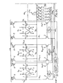
- ML is a left memory cell group and MR is a right memory cell group, and word decoders are provided between the memory cell groups in correspondence to cell rows.
- word decoder WDk of the kth row is indicated.
- the word decoder WDk drives in common all the bits on the word line WLk.
- n memory cells CL1 to CLn are connected along the word line WLk and each of those memory cells comprises a pair of FETs (1, 2) which operate in the complementary mode and a pair of transfer FETs (7, 8).
- To the pairs of FETs (1, 2) of the memory cells respective bit line pairs (BL1, BL1 B) to (BLn, BLnB) are connected.
- the bit lines BL1, BL1B) to (BLn, BLnB) respectively output complementary logical bit data.
- the complementary bits of this bit data on respective bit line pairs are led to respective pairs of FETs (3, 4) connected to respective column decoders CDL1 to CDLn, and input to a sense circuit 21 after being wire ORed for all FETs (3, 4) associated with all column decoders CDL1 to CDLn, and output as a memory output Mout via an output circuit 22.
- the FETs (5, 6) inserted in each of the bit lines BL1B, BL1...BLnB, BLn are load FETs.
- CDR1 to CDRn are column decoders
- BR1, BR1B...BRn, BRnB are bit lines
- CR1 to CRn are memory cells.
- the word decoder WDk connected to that memory cell CL1 is selected from among the word decoders by a word address ADWk.
- the word address ADWk consists of address bits AO (or AO), A1 (or A1), A2 (or A2), A3 (or A3), and A4 (or A4) when the number of memory cells in the column direction is 32.
- word decoder WDk When the word decoder WDk is specified by the word address ADWk, all FETs (9, 10, 11, 12, and 13) constituting word decoder WDk become OFF and therefore word line WDk becomes of "H" (high) level so that the transfer FETs (7, 8) of the corresponding memory cells become ON. Thereby, bit currents iL1 to iLn and iR1 to iRn flow to each FET (7 or 8) on the side of that FET (1 or 2) storing data "L” in each pair of FETs (1, 2) of the memory cells CL1 to CLn and CR1 to CRn on the word line WLk, from power supply Vcc to power supply Vss.
- the column decoder CDL1 corresponding to the relevant memory cell CL1 from among all the column decoders (CDL1 to CDLn and CDR1 to CDRn) is designated by a column address ADCL1, and the data stored in the memory cell CL1 is output through the sense circuit 21 and output circuit 22 via the bit lines (BL1, BL1B).
- the Column address ADCL consists of address bits A5 (or A5), A6 (or A6), A7 (or A7) A8 (or A8) and A9 (or A9) when the number of memory cells in the word direction is 32.
- the total (unwanted) bit current becomes very heavy and is as high as indicated by the following equation. This means that power consumption becomes high and a high speed operation is considerably restricted because all memory cells must be driven at one time.
- FIG. 2 shows an embodiment of the present invention.
- a left memory cell group (ML) drive gate 31 and a right memory cell group (MR) drive gate 31 R are provided on the left and right sides of each word decoder, and these left and right memory cell group drive gates 31 R and 31 L are closed alternatively.
- the gates 31 L and 31 R receive respectively the lowest (last) column address bit A9 and its complementary bit A9, for example, which discriminates whether a memory cell specified for access is of the left or the right memory cell group (MR, ML). Since memory cell CL1 of the left memory cell group ML is designated, the address bit A9 is logic "1" i.e. "H” level. Thus, the left memory cell group drive gate 31 opens and simultaneously the right memory cell group drive gate 31R closes. Thus the right side of the word line WLk is not driven and the current indicated by in the total bit current above becomes zero. On the other hand, if a memory cell in the right memory cell group MR is accessed, the address bit A9 is logic "0" i.e.
- the right and left memory cell group drive gates 31R and 31L L respectively comprise transistors (32, 33) and transistors (34, 35).
- the transistor 32 and transistor 34 are inserted in series in the word line WDk but transistor 33 and transistor 35 are connected in parallel betweenbeginn line WDk and power supply Vss.
- the desired gate function can be obtained by transistor 32 and transistor 34 alone, but it is desirable to keep the corresponding right or left word line forcibly to a specified potential (Vss) by means of transistor 33 or 35 which becomes ON simultaneously with the transistors 34 or 32 when they become ON, in order to prevent that right or left word line floating (i.e. for clamping), which floating could result in erroneous operation when the transistor 32 or 34 becomes OFF.
- the transistors 32 and 33 are ON or OFF complementarily and the transistors 34 and 35 also are ON or OFF complementarily.
- transistors 32 and 34 must become ON or OFF alternatively and therefore they require the discrimination results A9 and A9 as input signals.
- the memory cells in the right side can be put into the not-driven condition without being placed in a floating mode.
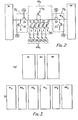
- Figure 3 shows examples or arrangement patterns of word decoders and memory cell groups to which the present invention can be applied.
- FIG 3 shows an arrangement pattern in which two word decoders (WD A , WD B ) are provided between a first right memory cell group MR A and a first left memory cell group ML A , and a second right memory cell group MR B and a second left memory cell group ML B , respectively.
- embodiments of the present invention can realise semiconductor memory circuits in which power consumption is reduced to almost one half that of a existing circuits and which are also suitable for high speed operation.
- a semiconductor memory circuit embodying this invention is provided with a right memory cell group and a left memory cell group, divided to the right and left, and word decoders corresponding to respective rows of the memory cell groups which are located between the right and left memory cell groups and which specify an address in the word direction of the memory cell groups, and column decoders corresponding to respective columns and which specify an address in the bit direction of the memory cell groups.
- the semiconductor memory circuit comprises right and left memory cell group selection and drive gates provided for each word decoder and means for discriminating whether a memory cell to be accessed is of the right or left memory cell groups.
Landscapes
- Engineering & Computer Science (AREA)
- Microelectronics & Electronic Packaging (AREA)
- Computer Hardware Design (AREA)
- Static Random-Access Memory (AREA)
- Semiconductor Memories (AREA)
Description
- This invention relates to a semiconductor memory circuit, and more particularly to a static type semiconductor memory circuit.
- A semiconductor memory circuit, for example, a static type semiconductor memory circuit basically comprises many memory cells, for storing data, arranged in a matrix, word decoders for specifying the address of memory cells in the matrix from the word direction and column decoders for specifying the address of memory cells from the colomn direction. These word decoders and column decoders are respectively arranged along one side of the memory cell matrix in a vertical direction and along one side of the memory cell matrix in a lateral direction, and can enable the data stored in one memory cell, specified in both vertical and lateral directions, to be read. In reality, the memory cells are divided into two groups:- a right memory cell group and a left memory cell group, and word decoders are arranged centrally between the right and left memory cell groups (see e.g. DE-A-2853204). This is because if the word decoders were arranged in the vertical direction on one side of the memory cell matrix a voltage drop between one end and the other of polysilicon electrodes extending in the lateral direction across the matrix from the decoders would be of considerable size. Therefore, the word decoders are located centrally between the right and left memory cell groups in order to reduce a voltage drop along such an electrode by half, and to share equally the voltage drop between the right and left memory cell groups, thereby improving memory functions.
- However, a semiconductor memory circuit as mentioned above has inevitable disadvantages. the first disadvantage is high power consumption, and the second disadvantage is that output operation speed cannot be made very high even at the expense of such disadvantageous high power consumption. This latter disadvantage arises as follows. Namely, bit current flows to all memory cells storing data "L" (low level data) among memory cells associated with one selected word decoder, as a result of the structure of the semiconductor memory circuit, without regard to whether or not the relevant memory cells are also selected in the bit direction. Therefore, if that bit current, which is mostly unwanted and used in vain, can be at least reduced by half, this would be a measure going a considerable way towards removing such disadvantage above.
- US-A-3 848 237 discloses a dynamic memory with X-decoders between left and right dynamic cell arrays. Lines extending from these decoders include left and right side switches, and there are provided left and right drivers for controlling those switches.
- According to the present invention there is provided a semiconductor memory circuit of static type having a plurality of word lines each extending through right and left memory cell groups and corresponding respectively to respective rows of the memory cell groups, and having word decoders, corresponding to respective word lines, located between the right and left memory cell groups, each memory cell having a pair of transfer transistors having gates connected to one of the word lines, characterised in that the semiconductor memory circuit further comprises a respective right memory cell group selection and drive gate and a respective left memory cell group selection and drive gate provided for each word decoder and including discriminating means, for discriminating to which of the right and left memory cell groups a memory cell to be accessed belongs, and providing a discrimination result, either the right or the left memory cell group selection and drive gate being closed in dependence upon the discrimination result, and each memory call group selection and drive gate further including a clamping means, connected respectively between a voltage source and the right and left memory cell groups, for clamping the corresponding word line on the side of the closed gate.
- An embodiment of the present invention can provide a semiconductor memory circuit which can provide for a reduced bit current and thereby reduced power consumption.
- An embodiment of the present invention can provide a semiconductor memory circuit which can reduce power consumption by means of a simple additional construction. Further, an embodiment of the present invention can provide a semiconductor memory circuit which can provide for speed up of output operation.
- An embodiment of the present invention provides discrimination means which discriminate to which of right and left memory cell groups a specified memory cell belongs, right and left memory cell group drive gates provided for each word decoder, one or other of the right and left memory cell group drive gates being closed in accordance with the result of discrimination of the discrimination means.
- Reference is made, by way of example, to the accompanying drawings, in which:-
- Figure 1 is a schematic circuit diagram for assistance in explanation of the structure and operation of a general semiconductor memory circuit;
- Figure 2 is a schematic circuit diagram illustrating an embodiment of the present invention; and
- Figure 3 is a schematic diagram illustrating arrangement patterns of word decoders and memory cell groups different from that of Figure 2 to which embodiments of the present invention can also be applied.
- In Figure 1, ML is a left memory cell group and MR is a right memory cell group, and word decoders are provided between the memory cell groups in correspondence to cell rows. However, in Figure 1, only word decoder WDk of the kth row is indicated. The word decoder WDk drives in common all the bits on the word line WLk.
- Considering the left memory cell group ML, n memory cells CL1 to CLn are connected along the word line WLk and each of those memory cells comprises a pair of FETs (1, 2) which operate in the complementary mode and a pair of transfer FETs (7, 8). To the pairs of FETs (1, 2) of the memory cells respective bit line pairs (BL1, BL1 B) to (BLn, BLnB) are connected. The bit lines BL1, BL1B) to (BLn, BLnB) respectively output complementary logical bit data. The complementary bits of this bit data on respective bit line pairs are led to respective pairs of FETs (3, 4) connected to respective column decoders CDL1 to CDLn, and input to a
sense circuit 21 after being wire ORed for all FETs (3, 4) associated with all column decoders CDL1 to CDLn, and output as a memory output Mout via anoutput circuit 22. The FETs (5, 6) inserted in each of the bit lines BL1B, BL1...BLnB, BLn are load FETs. - The abovementioned structure is also adopted for the right memory cell group MR, where CDR1 to CDRn are column decoders, BR1, BR1B...BRn, BRnB are bit lines, CR1 to CRn are memory cells.
- If an address is specified for memory cell CL1 (the memory cell connected to the first bit lines (BL1, BL1B) within the left memory cell group ML), the word decoder WDk connected to that memory cell CL1 is selected from among the word decoders by a word address ADWk.
- The word address ADWk consists of address bits AO (or AO), A1 (or A1), A2 (or A2), A3 (or A3), and A4 (or A4) when the number of memory cells in the column direction is 32.
- When the word decoder WDk is specified by the word address ADWk, all FETs (9, 10, 11, 12, and 13) constituting word decoder WDk become OFF and therefore word line WDk becomes of "H" (high) level so that the transfer FETs (7, 8) of the corresponding memory cells become ON. Thereby, bit currents iL1 to iLn and iR1 to iRn flow to each FET (7 or 8) on the side of that FET (1 or 2) storing data "L" in each pair of FETs (1, 2) of the memory cells CL1 to CLn and CR1 to CRn on the word line WLk, from power supply Vcc to power supply Vss. Then, the column decoder CDL1 corresponding to the relevant memory cell CL1 from among all the column decoders (CDL1 to CDLn and CDR1 to CDRn) is designated by a column address ADCL1, and the data stored in the memory cell CL1 is output through the
sense circuit 21 andoutput circuit 22 via the bit lines (BL1, BL1B). The Column address ADCL, consists of address bits A5 (or A5), A6 (or A6), A7 (or A7) A8 (or A8) and A9 (or A9) when the number of memory cells in the word direction is 32. - Focusing attention on the bit currents, even when an address is specified only for memory cell CL1, unwanted and useless bit currents also flow into all memory cells other than the memory cell CL1.
- The total (unwanted) bit current becomes very heavy and is as high as indicated by the following equation.

- In an embodiment of the present invention, some additional circuits are connected to each word decoder with a view to reducing the total amount of the bit current by half. Figure 2 shows an embodiment of the present invention. In this Figure, a left memory cell group (ML) drive gate 31 and a right memory cell group (MR)
drive gate 31 R are provided on the left and right sides of each word decoder, and these left and right memory cellgroup drive gates - The
gates group drive gate 31R closes. Thus the right side of the word line WLk is not driven and the current indicated by
group drive gate 31 R opens and simultaneously the left memory cellgroup drive gate 31 L closes. Therefore, the left part of the word line WLk is not driven and the current indicated by
- The right and left memory cell
group drive gates transistor 32 andtransistor 34 are inserted in series in the word line WDk buttransistor 33 andtransistor 35 are connected in parallel between wird line WDk and power supply Vss. In principle, the desired gate function can be obtained bytransistor 32 andtransistor 34 alone, but it is desirable to keep the corresponding right or left word line forcibly to a specified potential (Vss) by means oftransistor transistors transistor transistors transistors - In addition,
transistors transistor 34 becomes ON because A9="H" and thetransistor 35 becomes OFF because A9="L". On the other hand, thetransistor 32 becomes OFF because A9="L" and thetransistor 33 becomes ON because A9="H". In this case, the memory cells in the right side can be put into the not-driven condition without being placed in a floating mode. - Figure 3 shows examples or arrangement patterns of word decoders and memory cell groups to which the present invention can be applied.
- In Figure 3, (a) shows an arrangement pattern corresponding to Figure 1.
- In Figure 3, (b) shows an arrangement pattern in which two word decoders (WDA, WDB) are provided between a first right memory cell group MRA and a first left memory cell group MLA, and a second right memory cell group MRB and a second left memory cell group MLB, respectively.
- As explained above, embodiments of the present invention can realise semiconductor memory circuits in which power consumption is reduced to almost one half that of a existing circuits and which are also suitable for high speed operation.
- A semiconductor memory circuit embodying this invention is provided with a right memory cell group and a left memory cell group, divided to the right and left, and word decoders corresponding to respective rows of the memory cell groups which are located between the right and left memory cell groups and which specify an address in the word direction of the memory cell groups, and column decoders corresponding to respective columns and which specify an address in the bit direction of the memory cell groups. The semiconductor memory circuit comprises right and left memory cell group selection and drive gates provided for each word decoder and means for discriminating whether a memory cell to be accessed is of the right or left memory cell groups.
- Thereby, the right or left memory cell group selection and drive gates are closed alternatively in accordance with the discrimination result provided by the discrimination means.
Claims (3)
Applications Claiming Priority (2)
| Application Number | Priority Date | Filing Date | Title |
|---|---|---|---|
| JP16918779A JPS56101687A (en) | 1979-12-27 | 1979-12-27 | Semiconductor memory circuit |
| JP169187/79 | 1979-12-27 |
Publications (3)
| Publication Number | Publication Date |
|---|---|
| EP0032014A2 EP0032014A2 (en) | 1981-07-15 |
| EP0032014A3 EP0032014A3 (en) | 1983-08-24 |
| EP0032014B1 true EP0032014B1 (en) | 1987-07-08 |
Family
ID=15881839
Family Applications (1)
| Application Number | Title | Priority Date | Filing Date |
|---|---|---|---|
| EP80304529A Expired EP0032014B1 (en) | 1979-12-27 | 1980-12-16 | Semiconductor memory circuit |
Country Status (5)
| Country | Link |
|---|---|
| US (1) | US4393472A (en) |
| EP (1) | EP0032014B1 (en) |
| JP (1) | JPS56101687A (en) |
| DE (1) | DE3071990D1 (en) |
| IE (1) | IE52927B1 (en) |
Families Citing this family (20)
| Publication number | Priority date | Publication date | Assignee | Title |
|---|---|---|---|---|
| US4608672A (en) * | 1983-07-14 | 1986-08-26 | Honeywell Inc. | Semiconductor memory |
| US4611131A (en) * | 1983-08-31 | 1986-09-09 | Texas Instruments Incorporated | Low power decoder-driver circuit |
| JPS61199297A (en) * | 1985-02-28 | 1986-09-03 | Toshiba Corp | Semiconductor memory device |
| US5237532A (en) * | 1986-06-30 | 1993-08-17 | Kabushiki Kaisha Toshiba | Serially-accessed type memory device for providing an interleaved data read operation |
| JP3016392B2 (en) * | 1987-08-28 | 2000-03-06 | 株式会社日立製作所 | Static RAM |
| JPH0766669B2 (en) * | 1988-02-19 | 1995-07-19 | 日本電気株式会社 | Decoder buffer circuit |
| US5335336A (en) * | 1988-03-28 | 1994-08-02 | Hitachi, Ltd. | Memory device having refresh mode returning previous page address for resumed page mode |
| US5724540A (en) * | 1988-03-28 | 1998-03-03 | Hitachi, Ltd. | Memory system having a column address counter and a page address counter |
| JP2895488B2 (en) * | 1988-04-18 | 1999-05-24 | 株式会社東芝 | Semiconductor storage device and semiconductor storage system |
| US5016216A (en) * | 1988-10-17 | 1991-05-14 | Waferscale Integration, Inc. | Decoder for a floating gate memory |
| US5128897A (en) * | 1990-09-26 | 1992-07-07 | Sgs-Thomson Microelectronics, Inc. | Semiconductor memory having improved latched repeaters for memory row line selection |
| US5121358A (en) * | 1990-09-26 | 1992-06-09 | Sgs-Thomson Microelectronics, Inc. | Semiconductor memory with power-on reset controlled latched row line repeaters |
| US5119340A (en) * | 1990-09-26 | 1992-06-02 | Sgs-Thomson Microelectronics, Inc. | Semiconductor memory having latched repeaters for memory row line selection |
| US5388072A (en) * | 1992-04-10 | 1995-02-07 | International Business Machines Corporation | Bit line switch array for electronic computer memory |
| US6038634A (en) * | 1998-02-02 | 2000-03-14 | International Business Machines Corporation | Intra-unit block addressing system for memory |
| US6246630B1 (en) | 1998-02-02 | 2001-06-12 | International Business Machines Corporation | Intra-unit column address increment system for memory |
| US6118726A (en) * | 1998-02-02 | 2000-09-12 | International Business Machines Corporation | Shared row decoder |
| US6002275A (en) * | 1998-02-02 | 1999-12-14 | International Business Machines Corporation | Single ended read write drive for memory |
| US6407961B1 (en) * | 1998-06-11 | 2002-06-18 | Dsp Group, Ltd. | Dual access memory array |
| IL124863A (en) * | 1998-06-11 | 2004-05-12 | Dsp Group Ltd | Dual access memory array |
Family Cites Families (6)
| Publication number | Priority date | Publication date | Assignee | Title |
|---|---|---|---|---|
| US3848237A (en) * | 1973-02-20 | 1974-11-12 | Advanced Memory Syst | High speed mos random access read/write memory device |
| JPS5235951A (en) * | 1975-09-16 | 1977-03-18 | Nippon Telegr & Teleph Corp <Ntt> | Memory signal detection unit |
| US4074237A (en) * | 1976-03-08 | 1978-02-14 | International Business Machines Corporation | Word line clamping circuit and decoder |
| JPS6023432B2 (en) * | 1977-12-09 | 1985-06-07 | 株式会社日立製作所 | MOS memory |
| DE2842547A1 (en) * | 1978-09-29 | 1980-04-10 | Siemens Ag | CIRCUIT ARRANGEMENT FOR READING AND REGENERATING INFORMATION STORED IN A TRANSISTOR MEMORY ELEMENTS |
| US4453175A (en) * | 1979-09-19 | 1984-06-05 | Tokyo Shibaura Denki Kabushiki Kaisha | MOS Static RAM layout with polysilicon resistors over FET gates |
-
1979
- 1979-12-27 JP JP16918779A patent/JPS56101687A/en active Pending
-
1980
- 1980-12-16 DE DE8080304529T patent/DE3071990D1/en not_active Expired
- 1980-12-16 IE IE2649/80A patent/IE52927B1/en not_active IP Right Cessation
- 1980-12-16 EP EP80304529A patent/EP0032014B1/en not_active Expired
- 1980-12-18 US US06/217,803 patent/US4393472A/en not_active Expired - Lifetime
Also Published As
| Publication number | Publication date |
|---|---|
| DE3071990D1 (en) | 1987-08-13 |
| IE802649L (en) | 1981-06-27 |
| JPS56101687A (en) | 1981-08-14 |
| EP0032014A2 (en) | 1981-07-15 |
| EP0032014A3 (en) | 1983-08-24 |
| IE52927B1 (en) | 1988-04-13 |
| US4393472A (en) | 1983-07-12 |
Similar Documents
| Publication | Publication Date | Title |
|---|---|---|
| EP0032014B1 (en) | Semiconductor memory circuit | |
| EP0050022A2 (en) | Static type semiconductor memory device | |
| US4745579A (en) | Electrically erasable programmable logic array (EEPLA) | |
| KR0179361B1 (en) | Bitline segmentation in logic memory arrays c 16/06 | |
| EP0072845B1 (en) | Memory system having memory cells capable of storing more than two states | |
| US5933387A (en) | Divided word line architecture for embedded memories using multiple metal layers | |
| KR950010758B1 (en) | Dynamic memory | |
| KR890012312A (en) | Semiconductor memory | |
| RU2089943C1 (en) | Permanent storage | |
| US5396124A (en) | Circuit redundancy having a variable impedance circuit | |
| KR880000968A (en) | Semiconductor memory | |
| US5453950A (en) | Five transistor memory cell with shared power line | |
| US6362994B1 (en) | Memory architecture and decoder addressing | |
| US6038162A (en) | Semiconductor memory device | |
| EP0801397B1 (en) | Improvements in or relating to semiconductor memory devices | |
| US5757689A (en) | Semiconductor memory activated by plurality of word lines on same row | |
| EP0172112A2 (en) | Semiconductor memory device | |
| US5570312A (en) | SRAM cell using word line controlled pull-up NMOS transistors | |
| EP0565024B1 (en) | Row decoder for driving word line at a plurality of points thereof | |
| JPH0368479B2 (en) | ||
| EP0321847B1 (en) | Semiconductor memory capable of improving data rewrite speed | |
| EP0271283A2 (en) | Static semiconductor memory device having improved pull-up operation for bit lines | |
| US20040119105A1 (en) | Ferroelectric memory | |
| JPH041957B2 (en) | ||
| KR100335267B1 (en) | Semiconductor memory device reduces the consumption of sensing current |
Legal Events
| Date | Code | Title | Description |
|---|---|---|---|
| PUAI | Public reference made under article 153(3) epc to a published international application that has entered the european phase |
Free format text: ORIGINAL CODE: 0009012 |
|
| AK | Designated contracting states |
Designated state(s): DE FR GB NL |
|
| RBV | Designated contracting states (corrected) |
Designated state(s): DE FR GB NL |
|
| 17P | Request for examination filed |
Effective date: 19811027 |
|
| PUAL | Search report despatched |
Free format text: ORIGINAL CODE: 0009013 |
|
| AK | Designated contracting states |
Designated state(s): DE FR GB NL |
|
| GRAA | (expected) grant |
Free format text: ORIGINAL CODE: 0009210 |
|
| AK | Designated contracting states |
Kind code of ref document: B1 Designated state(s): DE FR GB |
|
| ET | Fr: translation filed | ||
| REF | Corresponds to: |
Ref document number: 3071990 Country of ref document: DE Date of ref document: 19870813 |
|
| PLBE | No opposition filed within time limit |
Free format text: ORIGINAL CODE: 0009261 |
|
| STAA | Information on the status of an ep patent application or granted ep patent |
Free format text: STATUS: NO OPPOSITION FILED WITHIN TIME LIMIT |
|
| 26N | No opposition filed | ||
| PGFP | Annual fee paid to national office [announced via postgrant information from national office to epo] |
Ref country code: GB Payment date: 19921013 Year of fee payment: 13 |
|
| PGFP | Annual fee paid to national office [announced via postgrant information from national office to epo] |
Ref country code: FR Payment date: 19921221 Year of fee payment: 13 |
|
| PGFP | Annual fee paid to national office [announced via postgrant information from national office to epo] |
Ref country code: DE Payment date: 19930226 Year of fee payment: 13 |
|
| PG25 | Lapsed in a contracting state [announced via postgrant information from national office to epo] |
Ref country code: GB Effective date: 19931216 |
|
| GBPC | Gb: european patent ceased through non-payment of renewal fee |
Effective date: 19931216 |
|
| PG25 | Lapsed in a contracting state [announced via postgrant information from national office to epo] |
Ref country code: FR Effective date: 19940831 |
|
| PG25 | Lapsed in a contracting state [announced via postgrant information from national office to epo] |
Ref country code: DE Effective date: 19940901 |
|
| REG | Reference to a national code |
Ref country code: FR Ref legal event code: ST |