EP0031769B1 - Perfectionnements aux échantillonneurs à très large bande - Google Patents
Perfectionnements aux échantillonneurs à très large bande Download PDFInfo
- Publication number
- EP0031769B1 EP0031769B1 EP80401825A EP80401825A EP0031769B1 EP 0031769 B1 EP0031769 B1 EP 0031769B1 EP 80401825 A EP80401825 A EP 80401825A EP 80401825 A EP80401825 A EP 80401825A EP 0031769 B1 EP0031769 B1 EP 0031769B1
- Authority
- EP
- European Patent Office
- Prior art keywords
- section
- frequency
- diode
- wave guide
- diodes
- Prior art date
- Legal status (The legal status is an assumption and is not a legal conclusion. Google has not performed a legal analysis and makes no representation as to the accuracy of the status listed.)
- Expired
Links
- 239000004020 conductor Substances 0.000 claims description 15
- 238000001228 spectrum Methods 0.000 claims description 9
- 230000005684 electric field Effects 0.000 claims description 6
- 230000006978 adaptation Effects 0.000 claims description 3
- 239000002184 metal Substances 0.000 claims description 3
- 230000000694 effects Effects 0.000 claims description 2
- 238000010586 diagram Methods 0.000 description 3
- 238000009826 distribution Methods 0.000 description 3
- 238000001914 filtration Methods 0.000 description 3
- 230000035559 beat frequency Effects 0.000 description 2
- 238000010009 beating Methods 0.000 description 2
- 238000004519 manufacturing process Methods 0.000 description 2
- 229910001369 Brass Inorganic materials 0.000 description 1
- 230000002745 absorbent Effects 0.000 description 1
- 239000002250 absorbent Substances 0.000 description 1
- 230000005540 biological transmission Effects 0.000 description 1
- 239000010951 brass Substances 0.000 description 1
- 239000003990 capacitor Substances 0.000 description 1
- 230000008878 coupling Effects 0.000 description 1
- 238000010168 coupling process Methods 0.000 description 1
- 238000005859 coupling reaction Methods 0.000 description 1
- 238000005520 cutting process Methods 0.000 description 1
- 230000003247 decreasing effect Effects 0.000 description 1
- 230000008030 elimination Effects 0.000 description 1
- 238000003379 elimination reaction Methods 0.000 description 1
- 238000005516 engineering process Methods 0.000 description 1
- 238000005259 measurement Methods 0.000 description 1
- 238000000034 method Methods 0.000 description 1
- 230000001902 propagating effect Effects 0.000 description 1
- 238000005070 sampling Methods 0.000 description 1
- 230000002459 sustained effect Effects 0.000 description 1
Images

Classifications
-
- G—PHYSICS
- G01—MEASURING; TESTING
- G01R—MEASURING ELECTRIC VARIABLES; MEASURING MAGNETIC VARIABLES
- G01R23/00—Arrangements for measuring frequencies; Arrangements for analysing frequency spectra
- G01R23/02—Arrangements for measuring frequency, e.g. pulse repetition rate; Arrangements for measuring period of current or voltage
- G01R23/14—Arrangements for measuring frequency, e.g. pulse repetition rate; Arrangements for measuring period of current or voltage by heterodyning; by beat-frequency comparison
-
- G—PHYSICS
- G01—MEASURING; TESTING
- G01R—MEASURING ELECTRIC VARIABLES; MEASURING MAGNETIC VARIABLES
- G01R23/00—Arrangements for measuring frequencies; Arrangements for analysing frequency spectra
- G01R23/16—Spectrum analysis; Fourier analysis
- G01R23/163—Spectrum analysis; Fourier analysis adapted for measuring in circuits having distributed constants
-
- H—ELECTRICITY
- H03—ELECTRONIC CIRCUITRY
- H03D—DEMODULATION OR TRANSFERENCE OF MODULATION FROM ONE CARRIER TO ANOTHER
- H03D9/00—Demodulation or transference of modulation of modulated electromagnetic waves
- H03D9/06—Transference of modulation using distributed inductance and capacitance
- H03D9/0608—Transference of modulation using distributed inductance and capacitance by means of diodes
- H03D9/0616—Transference of modulation using distributed inductance and capacitance by means of diodes mounted in a hollow waveguide
Definitions
- the present invention relates to a sampler covering a frequency band extending from the lower end of the frequency spectrum to several tens of gigahertz.
- a sampler in accordance with the use which is made of this term in metrology, a circuit comprising a local source of brief pulses, the spectrum of which consists of a discrete series of lines at multiple frequencies. of the recurrence frequency, associated with a non-linear element ensuring the beat with an applied signal whose frequency is to be determined.
- a low frequency output filter transmits the signal at the beat frequency (between that of the applied signal and that of a line of the spectrum of the local source) located in its bandwidth, for measurement. The determination of the frequency therefore requires the determination of the line which participated in the beat.
- the most expensive component is the sampler.
- the object of the present invention is the simple production of such a circuit, allowing a reduction in the cost price of the measuring assembly.
- the present invention is based on the use of the properties of waveguides, and more particularly of waveguides of rectangular section, as a high-pass filter. It is more particularly characterized in that the same waveguide section is used for the transmission of the pulses from the local source, for filtering by elimination of the low frequency components of the spectrum, for beating with the signal whose frequency is to be measured in a known circuit consisting of two diodes arranged in series in said guide section.
- a very wide-band sampler comprising: a source of brief pulses of frequency of recurrence F and of duration t determined to produce a spectrum of lines at multiple frequencies nF, n being an integer , that of recurrence, the source being constituted by means of a first diode defining said frequency of recurrence F and said duration t connected to a high frequency generator circuit annex; and a non-linear circuit coupled to the first diode and constituted by a second and a third diode connected in series by a conductor also connected to an input for receiving the signal to be analyzed and to an adaptation resistor, each of these second and third diodes being connected by its end other than that connected to the other diode to an associated output through a low-frequency circuit; the sampler being characterized in that it is produced in microwave circuit to cover a band going from continuous to several tens of gigahertz using a section of waveguide of rectangular straight sector and invariable
- the pulse source is a diode disposed in said guide section and placed in the same way as the mixing diodes in a cross section of the guide.
- the sampler according to the invention is particu lly simple to make, of reduced size and great robustness, which makes it particularly suitable for use as a measuring device.
- FIG. 1 shows the diagram equivalent to the sampling circuit.
- This circuit is known per se.
- the local oscillator has been depicted cutting pulses from the high frequency energy supplied by a source 2.
- the diode Di defines the shape and frequency of recurrence of the pulses. These are transmitted to the mixer circuit consisting essentially of diodes D 2 and D 3 connected in series.
- the coupling between D l and the mixer circuit is represented diagrammatically by arrows 3 and 4.
- Each of the diodes D 2 and D 3 is connected to a low frequency output S 2 and S 3 respectively by means of a pass-filter bottom, respectively F 2 and F 3 , consisting of an inductor and a capacitor.
- the diodes are self-polarized by resistors R '.
- the signal whose frequency is to be measured is applied in E l .
- the resistor R connected to the point common to the two diodes ensures the adaptation of the impedance in Ei.
- the diagram corresponds to a circuit well known to those skilled in the art, the invention residing in the realization of the circuit in waveguide technology.
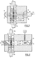
- FIG. 2 the pulse source, constituted by a diode D 1 , associated with the source 2 of sustained wave, is arranged in a wave guide 10 of rectangular section. Near the diode D 1 is disposed a load 11 absorbing the energy which propagates to the right in the guide. The energy propagating towards the left is transmitted in the guide 10 according to the arrows 3 and 4 towards the diodes D 2 and D 3 constituting the nonlinear circuit at a fixed level, independent of the frequency of the source 2.
- the part of guide between D l and D 2 -D 3 plays the role of a high-pass filter transmitting only the high frequency lines of the frequency spectrum of the pulses coming from the diode D I.
- the cutoff frequency of the guide is only defined by the dimensions a and b of its cross section.
- a second load 12 is placed to the left of the non-linear circuit so as to avoid any reflection of the energy which has not been used.
- the diodes D 2 and D 3 are mechanically integral with a bar 13 arranged along the large dimension of the guide, perpendicular to the direction of propagation, as can be seen more clearly in FIG. 3. One of the electrodes of each diode is in contact with this conductive bar.
- each of the diodes is connected to the central conductor, respectively 14 and 15, of a coaxial line ending in a coaxial output, respectively S 2 and S 3 .
- the filters F 2 and F 3 are constituted, as is well known, by the section of coaxial line disposed between the diode and the associated output. As is best seen in FIG. 3, the bar 13 is held parallel to the large walls of the rectangular guide 10 between the central conductor of the connector 16 constituting the input E 1 and the adapted load 17.
- the traces of the section planes of Figures 2 and 3 are shown in YY and XX respectively in the other figure.
- the diodes D 2 and D 3 are arranged in the rectangular cross section of the guide 10, not along the axis of symmetry, but at a distance from the small left wall equal to a quarter of the large dimension of the guide. This particular arrangement promotes the operation of the high frequency sampler circuit. Indeed, the energy which propagates in the guide 10 without attenuation consists of the upper part of the spectrum of the pulses formed by D i .
- Various modes of propagation are therefore established in the guide; the distribution of electric field in the cross section differs from one mode to another as is known.
- the location of the mixing diodes in the plane of symmetry of the guide corresponds to the location of the diodes at the maximum intensity of the electric field for the fundamental mode TE 01 .
- the location of the diodes at a distance from a small side equal to 1/4 of the large dimension of the guide places the diodes in the vicinity of the maximum electric field for order mode 2.
- the position chosen corresponds to a high intensity of the field distributions of the first three TEon modes.
- the positioning of the diodes is a compromise between bringing together a small side of the guide which corresponds to the maximum electric field of the higher modes and decreasing the value of the maximum field with the rank of the mode.
- the conductor 13 of the preferred embodiment which has just been described is a rod of circular section and of length equal to the largest dimension of the guide.
- the cross section of the conductor 13 influences the impedance at the input Ei of the sampler.
- Such a sampler delivers a constant level of ⁇ 2 dB when the frequency of the applied signal is a sine wave covering the frequency band between 0.1 and 24 GHz.
Landscapes
- Physics & Mathematics (AREA)
- General Physics & Mathematics (AREA)
- Electromagnetism (AREA)
- Engineering & Computer Science (AREA)
- Power Engineering (AREA)
- Mathematical Physics (AREA)
- Control Of Motors That Do Not Use Commutators (AREA)
- Measurement Of Resistance Or Impedance (AREA)
Applications Claiming Priority (2)
| Application Number | Priority Date | Filing Date | Title |
|---|---|---|---|
| FR7931798 | 1979-12-27 | ||
| FR7931798A FR2472757A1 (fr) | 1979-12-27 | 1979-12-27 | Perfectionnements aux echantillonneurs a tres large bande |
Publications (3)
| Publication Number | Publication Date |
|---|---|
| EP0031769A2 EP0031769A2 (fr) | 1981-07-08 |
| EP0031769A3 EP0031769A3 (en) | 1981-08-05 |
| EP0031769B1 true EP0031769B1 (fr) | 1984-03-14 |
Family
ID=9233203
Family Applications (1)
| Application Number | Title | Priority Date | Filing Date |
|---|---|---|---|
| EP80401825A Expired EP0031769B1 (fr) | 1979-12-27 | 1980-12-18 | Perfectionnements aux échantillonneurs à très large bande |
Country Status (4)
| Country | Link |
|---|---|
| US (1) | US4427938A (enExample) |
| EP (1) | EP0031769B1 (enExample) |
| DE (1) | DE3067062D1 (enExample) |
| FR (1) | FR2472757A1 (enExample) |
Families Citing this family (3)
| Publication number | Priority date | Publication date | Assignee | Title |
|---|---|---|---|---|
| US6242899B1 (en) | 1998-06-13 | 2001-06-05 | Lecroy Corporation | Waveform translator for DC to 75 GHz oscillography |
| US6407557B1 (en) * | 1998-08-27 | 2002-06-18 | Canon Kabushiki Kaisha | Process for measuring the electrical resistance of a resistive body for example for checking the conformity of a liquid product and devices for carrying out such a process |
| JP4130323B2 (ja) * | 2002-03-28 | 2008-08-06 | 株式会社東芝 | 高周波フィルタ及び高周波集積回路 |
Family Cites Families (4)
| Publication number | Priority date | Publication date | Assignee | Title |
|---|---|---|---|---|
| DE1061392B (de) * | 1955-08-20 | 1959-07-16 | Siemens Ag | Mischanordnung fuer sehr kurze elektromagnetische Wellen |
| US2832885A (en) | 1956-10-30 | 1958-04-29 | Brett Herbert | Superheterodyne receiver with local oscillator operating at intermediate frequency for simultaneously monitoring plural channels |
| DE1137486B (de) * | 1960-08-05 | 1962-10-04 | Felten & Guilleaume Gmbh | Gegentaktmischanordnung fuer Mikrowellen |
| US3609559A (en) | 1970-06-18 | 1971-09-28 | Bell Telephone Labor Inc | Coaxial microwave modulator |
-
1979
- 1979-12-27 FR FR7931798A patent/FR2472757A1/fr active Granted
-
1980
- 1980-12-05 US US06/213,580 patent/US4427938A/en not_active Expired - Lifetime
- 1980-12-18 DE DE8080401825T patent/DE3067062D1/de not_active Expired
- 1980-12-18 EP EP80401825A patent/EP0031769B1/fr not_active Expired
Also Published As
| Publication number | Publication date |
|---|---|
| FR2472757B1 (enExample) | 1983-01-28 |
| US4427938A (en) | 1984-01-24 |
| EP0031769A2 (fr) | 1981-07-08 |
| DE3067062D1 (en) | 1984-04-19 |
| EP0031769A3 (en) | 1981-08-05 |
| FR2472757A1 (fr) | 1981-07-03 |
Similar Documents
| Publication | Publication Date | Title |
|---|---|---|
| EP2156201B1 (fr) | Système d'émission d'impulsion électrique et dispositif de découplage capacitif pour un tel système | |
| EP0335767A1 (fr) | Dispositif pour réaliser une mesure de la teneur en eau d'un substrat, notamment de la peau | |
| EP0114140A1 (fr) | Filtre hyperfréquence accordable, à résonateurs diélectriques en mode TM010 | |
| FR3095303A1 (fr) | Ecran polariseur a cellule(s) polarisante(s) radiofrequence(s) large bande | |
| EP0048189A1 (fr) | Oscillateur à transistor comportant un résonateur diélectrique qui lui confère une stabilité maximale et un bruit minimal en très haute fréquence | |
| EP0031769B1 (fr) | Perfectionnements aux échantillonneurs à très large bande | |
| EP0084311A1 (fr) | Dispositif de protection d'un câble coaxial contre les impulsions parasites de basse fréquence et de forte puissance | |
| FR2704358A1 (fr) | Duplexeur de polarissation à guide d'ondes. | |
| FR3030909A1 (fr) | Antenne fil-plaque ayant un toit capacitif incorporant une fente entre la sonde d'alimentation et le fil de court-circuit | |
| Lim et al. | Design and test of an electric field sensor for the measurement of high-voltage nanosecond pulses | |
| EP2443467A1 (fr) | Dispositif de surveillance d'un poste electrique haute tension isole au gaz par mesure de decharges partielles | |
| EP0021872B1 (fr) | Tête hyperfréquence d'émission et de réception simultanées, émetteur-récepteur en ondes millimétriques et radar utilisant une telle tête | |
| EP0078188A1 (fr) | Dispositif hyperfréquence à large bande générateur des harmoniques d'ordre pair d'un signal incident, et utilisation d'un tel dispositif dans un système hyperfréquence | |
| EP1685389A1 (fr) | Capteur et ensemble de mesures hydrometriques | |
| EP0073165B1 (fr) | Commutateur d'ondes électromagnétiques | |
| FR2803692A1 (fr) | Transition de lignes dielectriques hybrides non rayonnantes et appareil incorporant cette transition | |
| FR2509535A1 (fr) | Filtre hyperfrequence comportant des troncons de lignes couples et des moyens de reglage | |
| JPH10500817A (ja) | 超広帯域アンテナ | |
| EP0005396B1 (fr) | Circuit hyperfréquence à cavité résonnante équipée de paires de diodes périphériques | |
| FR2515432A1 (fr) | Coupleur de puissance micro-onde de dimensions reduites | |
| EP0013223A1 (fr) | Dispositif de filtrage d'harmoniques pour émetteur radioélectrique | |
| FR2611989A1 (fr) | Dispositif hyperfrequence a diodes comportant une ligne triplaque | |
| EP0221608A1 (fr) | Oscillateur hyperfréquence modulé linéairement en fréquence et à coefficient de surtension externe élevé | |
| FR2500707A1 (fr) | Dispositif de traitement de materiaux par hyper-frequences a elements modulaires | |
| EP0769213A1 (fr) | Transformateur d'impedance a haute frequence |
Legal Events
| Date | Code | Title | Description |
|---|---|---|---|
| PUAI | Public reference made under article 153(3) epc to a published international application that has entered the european phase |
Free format text: ORIGINAL CODE: 0009012 |
|
| PUAL | Search report despatched |
Free format text: ORIGINAL CODE: 0009013 |
|
| AK | Designated contracting states |
Designated state(s): DE GB IT |
|
| AK | Designated contracting states |
Designated state(s): DE GB IT |
|
| 17P | Request for examination filed |
Effective date: 19820125 |
|
| ITF | It: translation for a ep patent filed | ||
| GRAA | (expected) grant |
Free format text: ORIGINAL CODE: 0009210 |
|
| RBV | Designated contracting states (corrected) |
Designated state(s): DE GB IT |
|
| AK | Designated contracting states |
Designated state(s): DE GB IT |
|
| REF | Corresponds to: |
Ref document number: 3067062 Country of ref document: DE Date of ref document: 19840419 |
|
| PGFP | Annual fee paid to national office [announced via postgrant information from national office to epo] |
Ref country code: DE Payment date: 19841022 Year of fee payment: 5 |
|
| PLBE | No opposition filed within time limit |
Free format text: ORIGINAL CODE: 0009261 |
|
| STAA | Information on the status of an ep patent application or granted ep patent |
Free format text: STATUS: NO OPPOSITION FILED WITHIN TIME LIMIT |
|
| 26N | No opposition filed | ||
| GBPC | Gb: european patent ceased through non-payment of renewal fee | ||
| PG25 | Lapsed in a contracting state [announced via postgrant information from national office to epo] |
Ref country code: DE Effective date: 19860902 |
|
| PG25 | Lapsed in a contracting state [announced via postgrant information from national office to epo] |
Ref country code: GB Effective date: 19881118 |