EP0031751B1 - Générateur de tension codée à transfert de charges, codeur et décodeur analogique-numérique comportant un tel générateur - Google Patents
Générateur de tension codée à transfert de charges, codeur et décodeur analogique-numérique comportant un tel générateur Download PDFInfo
- Publication number
- EP0031751B1 EP0031751B1 EP80401781A EP80401781A EP0031751B1 EP 0031751 B1 EP0031751 B1 EP 0031751B1 EP 80401781 A EP80401781 A EP 80401781A EP 80401781 A EP80401781 A EP 80401781A EP 0031751 B1 EP0031751 B1 EP 0031751B1
- Authority
- EP
- European Patent Office
- Prior art keywords
- charges
- charge
- generator
- transfer
- voltage
- Prior art date
- Legal status (The legal status is an assumption and is not a legal conclusion. Google has not performed a legal analysis and makes no representation as to the accuracy of the status listed.)
- Expired
Links
- 238000002347 injection Methods 0.000 claims description 14
- 239000007924 injection Substances 0.000 claims description 14
- 239000000758 substrate Substances 0.000 claims description 7
- 238000009792 diffusion process Methods 0.000 claims description 6
- 238000009826 distribution Methods 0.000 claims description 4
- 238000002513 implantation Methods 0.000 claims description 3
- LFQCEHFDDXELDD-UHFFFAOYSA-N tetramethyl orthosilicate Chemical compound CO[Si](OC)(OC)OC LFQCEHFDDXELDD-UHFFFAOYSA-N 0.000 description 17
- 239000003990 capacitor Substances 0.000 description 4
- 238000010586 diagram Methods 0.000 description 4
- 238000002955 isolation Methods 0.000 description 4
- 239000004065 semiconductor Substances 0.000 description 4
- 238000006243 chemical reaction Methods 0.000 description 3
- 230000036316 preload Effects 0.000 description 3
- 238000000034 method Methods 0.000 description 2
- 244000045947 parasite Species 0.000 description 2
- 230000000737 periodic effect Effects 0.000 description 2
- 238000000926 separation method Methods 0.000 description 2
- 241000607057 Stenodus Species 0.000 description 1
- 240000008042 Zea mays Species 0.000 description 1
- 230000004888 barrier function Effects 0.000 description 1
- 230000001066 destructive effect Effects 0.000 description 1
- 230000008520 organization Effects 0.000 description 1
- 238000005036 potential barrier Methods 0.000 description 1
- 238000005096 rolling process Methods 0.000 description 1
- 208000006379 syphilis Diseases 0.000 description 1
- 238000009827 uniform distribution Methods 0.000 description 1
Images

Classifications
-
- H—ELECTRICITY
- H03—ELECTRONIC CIRCUITRY
- H03M—CODING; DECODING; CODE CONVERSION IN GENERAL
- H03M1/00—Analogue/digital conversion; Digital/analogue conversion
-
- H—ELECTRICITY
- H03—ELECTRONIC CIRCUITRY
- H03M—CODING; DECODING; CODE CONVERSION IN GENERAL
- H03M1/00—Analogue/digital conversion; Digital/analogue conversion
- H03M1/12—Analogue/digital converters
- H03M1/14—Conversion in steps with each step involving the same or a different conversion means and delivering more than one bit
Definitions
- the present invention relates to a coded voltage generator with charge transfer. It also relates to digital analog encoders and decoders comprising such a generator.
- the voltages V R and V R can be generated by networks of resistance or capacities whose values vary according to the powers of 2. This is the case for example in an article in the names of McCreary and Gray, which was published in the journal IEEE Journal of Solid- State Circuits, volume SC 10, N ° 6, December 1975, pages 371 to 385.
- the coded voltage generator according to the present invention also uses the redistribution of the charges but differs completely in its structure from the known device previously described.
- the generator according to the invention has all the advantages of the device according to FR-A-2 343 369 from the point of view of the reduced bulk and speed in particular. In addition, it has increased precision compared to the device according to FR-A-2 343 369.
- the quantities of charges Q R / 2, Q R / 2 2 ... Q R / 2 n are obtained see Figures 3 to 5 using two storage electrodes separated by a transfer electrode.
- a quantity of charges Q R is stored under one of the storage electrodes.
- the redistribution of the charges under the two storage electrodes, then their separation by the transfer electrode makes it possible to obtain Q R / 2 under each storage electrode.
- the charges under one of the storage electrodes are removed and a redistribution is then carried out, followed by a separation which makes it possible to obtain Q R / 4, and so on.
- the generator according to the invention in the case where the voltage V x is available and the coefficients a o ... a n are unknown, it is possible to avoid any reference voltage source outdoor, convert the voltage to be coded V x into a quantity of charges Q x using a charge injection device identical to that which is used to generate 2Q R. A reading of Q x , ie V Lx , is then carried out using a device identical to that which is used to read the charges under G 2 and G 4 . The advantage of the conversion, then of the reading of Q x is to compare signals V Lx and V Ri having the same continuous component and the same amplitude scale.
- the generator according to the invention has the advantage of being able to be used in analog-digital coders or decoders as described in the article under the names of Gray and Hodges, published under the title “All MOS analogic-digital conversion techniques” published in the journal IEEE Transactions on circuits and systems, volume CAS-25, number 7, July 78, pages 482 to 489.
- Figure 1 shows a top view of the charge transfer device constituting the generator according to the invention and the electrical diagram of the device consisting of MOS transistors, capacitors and resistances associated therewith. ''
- This charge transfer device is preferably of the C.C.D. (Charge Coupled Devices).
- the transfer of the charges can be done on the surface or in volume.
- the active area of the semiconductor substrate where the transfer and storage of the charges takes place is located inside line 1 in broken lines. Outside the zone delimited by this line, an overdoping of the substrate raises the inversion threshold and thus opposes any storage of the charges.
- a diode De which makes it possible to introduce a reference charge 2Q R under a storage grid G e by means of a transfer grid T 0 .
- the diode De and the gates T 0 and G e constitute the device for injecting the reference charge 2Q R into the generator.
- the diode De is also used for the removal of excess charges during the operation of the generator.
- the grid G e is followed by a transfer grid T 1 and a storage grid G 0 .
- an isolation diffusion advances, at half the width of the active charge transfer zone in order to pre-share the charge stored under G o into two equal charge quantities.
- This isolation diffusion divides the active area after G o into two parallel channels, generally of the same width.
- G 1 and G 2 located on each channel after Go and separated from Go by the transfer grids T 2 and T 3 , two quantities of charges will be transferred equal to half the charge stored under G o .
- This sharing of a quantity of charges by a diffused area is known from the prior art.
- One of the channels therefore ends with the storage grid G 2 , while the other channel comprises after the storage grid G 1 two storage grids G 3 and G 4 and three transfer grids, T 4 between G 1 and G 3 , Ts between G 3 and G 4 and T e between G 4 and a collector diode D c .
- the collecting diode D c which terminates the channel is connected to a direct voltage V DD and allows the charges to be discharged at the end of processing of a sample V x or of a series a 0 ... a n .
- the grids G 2 and G 4 or the grid G 4 only are connected at a point P to a device for reading the charges which performs a reading non-destructive of the charges stored under G 2 and G 4 or under G 4 only.
- This reading device can be a device for reading current charges known in the prior art, such as that described by French patent application No. 77.13857 published under No. 2,389,899 in the name of THOMSON- CSF.
- the potential of point P is kept constant during the arrival of the charges thanks to a MOS transistor Q 2 , connected between point P and a point A.
- the transistor Q 2 controlled by a periodic clock signal ⁇ 2 , is then finds polarized in saturation.
- the current flowing through Q 2 during the inflow of charges is integrated into a capacitor C A connected between point A and ground.
- the voltage at point A is read by a MQS or TMOS Q 5 transistor mounted as a follower, the gate of which is connected to point A, one of whose electrodes is connected to a voltage V DD and whose other electrode supplies the voltage reading across a resistor R s .
- the TMOS Q 5 can be replaced to read the voltage at point A by an operational gain amplifier I.
- a TMOS Q 3 is also connected, the grid of which is connected to B.
- a capacitor C B is connected between point B and the clock signal ⁇ 2 .
- a TMOS Q 4 is connected between point B and the voltage V DD , the gate of Q 4 is also connected to V DD .
- a TMOS Q 1 is connected between the grids G 2 and G 4 and the mass or between the grid G 2 only and the mass.
- the TMOS Q 1 is controlled by a periodic clock signal ⁇ 1 and causes when it conducts the resetting of the gates to which it is connected.
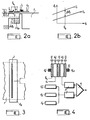
- the gates T 0 and G e receive the same voltage V GE , as shown in FIG. 2a which represents a sectional view of the device for injecting the charges and the surface potentials when the charge 2Q R is stored under G e .
- the quantity of reference charges 2QR is stable at first order, that is to say independent of variations in the voltage V GE applied to T 0 and G E , if the surface potential curves as a function of the voltage of this couple of grids are parallel.
- the threshold voltages are adjusted under T 0 and G e by implantation 5 under T 0 so that the barrier height ⁇ Q s is independent at first order of V GE .
- FIG. 2b represents the curves obtained for To and G e .
- T 4 and G 3 are set to zero and T 5 to an intermediate fixed potential, which corresponds to the transfer of a possible charge from G 3 to G 4 .
- the grids G 1 and G 2 preferably have an area equal to half that of G 0 .
- the charge Q R / 2 i is transferred from G 2 to Go. Before being able to transfer this charge again under the grids G 1 and G 2 to divide it by 2, it is essential that it has had time to distribute itself uniformly under G o .
- a grid G 0 is used whose width perpendicular to the direction of charge transfer is relatively large, of the order of 300 ⁇ m for example. The time for homogeneous distribution of a charge under an electrode of such a width is relatively long. To reduce this distribution time significantly, there is available over the entire width of G o a diffused zone of the type opposite to that of the semiconductor substrate 1.
- the voltage to be coded V x can be converted into a quantity of charges Q x using an injection device identical to that which is used to generate 2Q R.
- This device is shown in FIG. 4 and includes a diode D e 'followed by a transfer grid To' connected to Vce and a storage grid G e 'connected to V x .
- a reading of Q x is then carried out on a storage grid G 0 'adjacent to the injection device using a reading device identical to that which is used to read the charges under G 2 and G 4 .
- the generation of Q x must be done for the determination of each coefficient a i .
- the surface of G e ′ is preferably chosen to be identical to that of G e .
- the maximum load 2Q R which can be processed by the generator is then introduced under G e 'when V x equals V GE .
- the voltage excursion on G e 'then goes from V 0 to V 0 + V GE .
- the quantities of charges under G e 'therefore vary between Q 0 and Q 0 + 2Q R.
- the 2Q R , Q x + Q 0 and Q 0 injection devices must be close enough to each other on the semiconductor substrate to avoid variations in the technological parameters from one device to another with regard to the threshold voltage , the oxide thickness, etc. Having taken these precautions, it is possible to avoid the use of an external reference voltage source.
Landscapes
- Engineering & Computer Science (AREA)
- Theoretical Computer Science (AREA)
- Solid State Image Pick-Up Elements (AREA)
- Analogue/Digital Conversion (AREA)
- Semiconductor Memories (AREA)
Applications Claiming Priority (2)
| Application Number | Priority Date | Filing Date | Title |
|---|---|---|---|
| FR7931801A FR2474257A1 (fr) | 1979-12-27 | 1979-12-27 | Generateur de tension codee a transfert de charges, codeur et decodeur analogique-numerique comportant un tel generateur |
| FR7931801 | 1979-12-27 |
Publications (2)
| Publication Number | Publication Date |
|---|---|
| EP0031751A1 EP0031751A1 (fr) | 1981-07-08 |
| EP0031751B1 true EP0031751B1 (fr) | 1983-05-04 |
Family
ID=9233206
Family Applications (1)
| Application Number | Title | Priority Date | Filing Date |
|---|---|---|---|
| EP80401781A Expired EP0031751B1 (fr) | 1979-12-27 | 1980-12-12 | Générateur de tension codée à transfert de charges, codeur et décodeur analogique-numérique comportant un tel générateur |
Country Status (5)
| Country | Link |
|---|---|
| US (1) | US4350976A (https=) |
| EP (1) | EP0031751B1 (https=) |
| JP (1) | JPS56100521A (https=) |
| DE (1) | DE3062988D1 (https=) |
| FR (1) | FR2474257A1 (https=) |
Families Citing this family (5)
| Publication number | Priority date | Publication date | Assignee | Title |
|---|---|---|---|---|
| US4555770A (en) * | 1983-10-13 | 1985-11-26 | The United States Of America As Represented By The Secretary Of The Air Force | Charge-coupled device Gaussian convolution method |
| FR2597647B1 (fr) * | 1986-04-18 | 1992-06-12 | Thomson Csf | Registre a decalage a transfert de charge muni d'un dispositif de lecture en tension sur diode flottante |
| US5113365A (en) * | 1989-05-16 | 1992-05-12 | Massachusetts Institute Of Technology | Method and charge coupled apparatus for algorithmic computations |
| JP3028074B2 (ja) * | 1997-05-26 | 2000-04-04 | 日本電気株式会社 | 電荷転送素子とその駆動方法 |
| US6556589B2 (en) * | 1998-04-17 | 2003-04-29 | Advanced Micro Devices, Inc. | Network transceiver for steering network data to selected paths based on determined link speeds |
Family Cites Families (9)
| Publication number | Priority date | Publication date | Assignee | Title |
|---|---|---|---|---|
| JPS5644613B2 (https=) * | 1972-03-02 | 1981-10-21 | ||
| US3906488A (en) * | 1974-02-14 | 1975-09-16 | Univ California | Reversible analog/digital (digital/analog) converter |
| JPS5267250A (en) * | 1975-11-03 | 1977-06-03 | Gen Electric | Analoggtoodigital converter |
| US4087812A (en) * | 1975-12-23 | 1978-05-02 | International Business Machines Corporation | Digital-to-analog and analog-to-digital converter circuit |
| US4099175A (en) * | 1976-10-29 | 1978-07-04 | International Business Machines Corporation | Charge-coupled device digital-to-analog converter |
| US4206446A (en) * | 1977-05-23 | 1980-06-03 | Rca Corporation | CCD A-to-D converter |
| US4306221A (en) * | 1977-06-02 | 1981-12-15 | Hughes Aircraft Company | Charge-coupled analog-to-digital converter |
| US4213120A (en) * | 1978-03-06 | 1980-07-15 | Westinghouse Electric Corp. | CCD Digital-to-analog converter |
| US4164734A (en) * | 1978-06-26 | 1979-08-14 | Hughes Aircraft Company | Charge transfer multiplying feedback A/D converter |
-
1979
- 1979-12-27 FR FR7931801A patent/FR2474257A1/fr active Granted
-
1980
- 1980-12-10 US US06/215,134 patent/US4350976A/en not_active Expired - Lifetime
- 1980-12-12 DE DE8080401781T patent/DE3062988D1/de not_active Expired
- 1980-12-12 EP EP80401781A patent/EP0031751B1/fr not_active Expired
- 1980-12-25 JP JP18296380A patent/JPS56100521A/ja active Pending
Also Published As
| Publication number | Publication date |
|---|---|
| JPS56100521A (en) | 1981-08-12 |
| DE3062988D1 (en) | 1983-06-09 |
| EP0031751A1 (fr) | 1981-07-08 |
| US4350976A (en) | 1982-09-21 |
| FR2474257B1 (https=) | 1982-01-15 |
| FR2474257A1 (fr) | 1981-07-24 |
Similar Documents
| Publication | Publication Date | Title |
|---|---|---|
| EP0038725B1 (fr) | Dispositif photosensible lu par transfert de charges, et caméra de télévision comportant un tel dispositif | |
| US4156818A (en) | Operating circuitry for semiconductor charge coupled devices | |
| FR2577366A1 (fr) | Reseau resistance | |
| EP0115225B1 (fr) | Procédé d'analyse d'un dispositif photosensible à transfert de ligne et dispositif de mise en oeuvre d'un tel procédé | |
| EP0031751B1 (fr) | Générateur de tension codée à transfert de charges, codeur et décodeur analogique-numérique comportant un tel générateur | |
| EP0169754B1 (fr) | Comparateur analogique à transfert de charge, et dispositifs utilisant un tel comparateur | |
| EP0230809B1 (fr) | Caméra thermique à balayage parallèle | |
| EP0068947B1 (fr) | Ensemble détecteur photonique, lecteur à transfert de charges adapté, et cible de prise de vues utilisant un tel ensemble | |
| EP0182679B1 (fr) | Dispositif photosensible à transfert de ligne muni d'amplificateurs de contre-réaction | |
| EP0038762B1 (fr) | Codeur analogique-numérique comportant un générateur de tension codée à transfert de charges | |
| FR2476916A1 (fr) | Dispositif de detection et de traitement de rayonnement electromagnetique | |
| EP0149948B1 (fr) | Perfectionnement aux dispositifs photosensibles à l'état solide | |
| FR2511545A1 (fr) | Dispositif semi-conducteur comportant un dispositif a couplage de charges a quatre phases | |
| EP0163554B1 (fr) | Accumulateur analogique | |
| EP0958545B1 (fr) | Circuit integrateur de charges photogenerees a linearite amelioree | |
| EP0323924B1 (fr) | Procédé et circuit de lecture à faible bruit pour matrice photosensible à transfert de ligne | |
| EP0012667B1 (fr) | Procédé de filtrage d'un signal électrique par transfert de charges dans un semi-conducteur et filtre à capacités commutées utilisant un tel procédé | |
| EP0325524B1 (fr) | Mémoire à transfert de charges et procédé de fabrication de cette mémoire | |
| EP0322303B1 (fr) | Dispositif de transfert de charges à abaissement de potentiel de transfert en sortie, et procédé de fabrication de ce dispositif | |
| EP0021908B1 (fr) | Dispositif inverseur de phase à transfert de charges et amplificateur différentiel comportant un tel dispositif | |
| EP0334735B1 (fr) | Dispositif de lecture des quantités de charges électriques fournies par des photodiodes à substrat semi-conducteur | |
| EP0019506B1 (fr) | Dispositif à transfert de charges de soustraction et de génération de quantités de charges | |
| EP0323925B1 (fr) | Duplicateur de charges pour dispositif à transfert de charges | |
| FR2462822A1 (fr) | Convertisseur analogique-numerique utilisant un dispositif a transfert de charges | |
| EP0017541B1 (fr) | Filtre transversal à transfert de charges électriques |
Legal Events
| Date | Code | Title | Description |
|---|---|---|---|
| PUAI | Public reference made under article 153(3) epc to a published international application that has entered the european phase |
Free format text: ORIGINAL CODE: 0009012 |
|
| AK | Designated contracting states |
Designated state(s): DE GB NL |
|
| 17P | Request for examination filed |
Effective date: 19810803 |
|
| GRAA | (expected) grant |
Free format text: ORIGINAL CODE: 0009210 |
|
| AK | Designated contracting states |
Designated state(s): DE GB NL |
|
| REF | Corresponds to: |
Ref document number: 3062988 Country of ref document: DE Date of ref document: 19830609 |
|
| PLBE | No opposition filed within time limit |
Free format text: ORIGINAL CODE: 0009261 |
|
| STAA | Information on the status of an ep patent application or granted ep patent |
Free format text: STATUS: NO OPPOSITION FILED WITHIN TIME LIMIT |
|
| 26N | No opposition filed | ||
| PGFP | Annual fee paid to national office [announced via postgrant information from national office to epo] |
Ref country code: NL Payment date: 19871231 Year of fee payment: 8 |
|
| PG25 | Lapsed in a contracting state [announced via postgrant information from national office to epo] |
Ref country code: NL Effective date: 19890701 |
|
| NLV4 | Nl: lapsed or anulled due to non-payment of the annual fee | ||
| PGFP | Annual fee paid to national office [announced via postgrant information from national office to epo] |
Ref country code: GB Payment date: 19901122 Year of fee payment: 11 |
|
| PGFP | Annual fee paid to national office [announced via postgrant information from national office to epo] |
Ref country code: DE Payment date: 19901126 Year of fee payment: 11 |
|
| PG25 | Lapsed in a contracting state [announced via postgrant information from national office to epo] |
Ref country code: GB Effective date: 19911212 |
|
| GBPC | Gb: european patent ceased through non-payment of renewal fee | ||
| PG25 | Lapsed in a contracting state [announced via postgrant information from national office to epo] |
Ref country code: DE Effective date: 19920901 |