EP0029896A2 - Kompakte fluoreszierende Lichtquelle mit metallisierten Elektroden - Google Patents
Kompakte fluoreszierende Lichtquelle mit metallisierten Elektroden Download PDFInfo
- Publication number
- EP0029896A2 EP0029896A2 EP80106189A EP80106189A EP0029896A2 EP 0029896 A2 EP0029896 A2 EP 0029896A2 EP 80106189 A EP80106189 A EP 80106189A EP 80106189 A EP80106189 A EP 80106189A EP 0029896 A2 EP0029896 A2 EP 0029896A2
- Authority
- EP
- European Patent Office
- Prior art keywords
- lamp
- high frequency
- conductor
- envelope
- discharge
- Prior art date
- Legal status (The legal status is an assumption and is not a legal conclusion. Google has not performed a legal analysis and makes no representation as to the accuracy of the status listed.)
- Granted
Links
Images

Classifications
-
- H—ELECTRICITY
- H01—ELECTRIC ELEMENTS
- H01J—ELECTRIC DISCHARGE TUBES OR DISCHARGE LAMPS
- H01J65/00—Lamps without any electrode inside the vessel; Lamps with at least one main electrode outside the vessel
- H01J65/04—Lamps in which a gas filling is excited to luminesce by an external electromagnetic field or by external corpuscular radiation, e.g. for indicating plasma display panels
- H01J65/042—Lamps in which a gas filling is excited to luminesce by an external electromagnetic field or by external corpuscular radiation, e.g. for indicating plasma display panels by an external electromagnetic field
- H01J65/046—Lamps in which a gas filling is excited to luminesce by an external electromagnetic field or by external corpuscular radiation, e.g. for indicating plasma display panels by an external electromagnetic field the field being produced by using capacitive means around the vessel
Definitions
- This invention relates to fluorescent light sources and, more particularly, to capacitively coupled compart fluorescent light sources wherein at least one of the power coupling conductors is a conductive coating disposed on an external surface of the lamp envelope.
- the incandescent lamp has been widely used, especially in interior lighting applications. While simple and inexpensive, the incandescent lamp has very low efficacies, typically producing 15 to 20 lumens per watt of electrical power. The operating life of the incandescent lamp is relatively short and unpredictable.
- the fluorescent lamp by contrast, exhibits a very long life and a high efficacy, typically 80 lumens per watt of electrical power. Fluorescent sources have been optimized for overhead lighting in the form of straight or circular tubes which are not well adapted to many lighting needs presently met by the incandescent lamp. While conventional electroded fluorescent lamps provide long life and high efficiency, they require large, heavy, and expensive ballasting circuits for operation at line frequencies.
- inductive coupling has been used to transfer high frequency electromagnetic power to a low pressure discharge containing a noble gas and mercury vapor.
- the discharge generates ultraviolet light which is converted to visible light by a phosphor coating on the lamp envelope.
- Inductive coupling generally utilizes a coil to generate within its volume and the surrounding region an alternating magnetic field and an associated electric field, the latter field lines generally defining a closed path within the conductive plasma discharge.
- the current flow within the discharge is such as to form a secondary current in relationship to the driving coil similar to the relationship between the secondary and primary windings of a transformer. Due to collisions, the secondary current in the plasma discharge is somewhat resistive and therefore lossy, part of the loss being con- "- verted to light. While the generation of light can be most efficiently accomplished by a uniform excitation of the plasma, the development of closed secondary current paths in the plasma results in non-uniform excitation. Therefore, inductive coupling is not an optimal method for light generation.
- Electrodeless fluorescent light sources utilizing inductive coupling have been disclosed in various U. S. Patents.
- a closed loop magnetic core transformer contained within a re-entrant cavity in the lamp envelope, induces a discharge in an electrodeless fluorescent lamp in U. S. Patent No. 4,005,330 issued January 25, 1977 to Glascock et al.
- Discharge is induced by a magnetic core coil within the envelope of an electrodeless fluorescent lamp in the light source disclosed in U. S. Patent No. 4.017,764 issued April 12, 1977 to Anderson.
- th 2 operating frequency is limited to about 50 KHz because of the lossy nature of magnetic materials at high frequency.
- An electrodeless fluorescent light source utilizing frequencies in the 100 MHz to 300 GHz range, was disclosed by Haugsjaa et al in pending U. S. Application Serial No. 959,823 filed November 13, 1978 and assigned to the assignee of the present invention.
- High frequency power typically at 915 MHz, is coupled to an ultraviolet- producing low pressure discharge in a phosphor-coated electrodeless lamp which acts as a termination load within a termination fixture.
- the excitation of a plasma by capacitive coupling produces a stable and uniform plasma, a condition conducive to maximal light generation.
- the electric field lines of the applied oscillatory electromagnetic signal originate on one external electrode, pass through the envelope containing the discharge and terminate on a second external electrode. No closed current paths exist within the plasma in contrast to the situation occurring in inductively coupled plasma discharges described hereinabove.
- Capacitive coupling of an electromagnetic pulse to a low pressure discharge in an elongated laser discharge tube is disclosed by Proud et al in pending U. S. Application Serial No. 20,576 filed March 15, 1979 and assigned to the assignee of the present invention.
- External electrodes are coupled to end portions of the laser discharge tube.
- the generation of a light emitting, low pressure discharge in a resonant device including an inner elec- t rode and a coaxial outer electrode is disclosed in U. S. Patent No. 4,063,132 issued December 13, 1977 to Proud e : al.
- the resonant cavity between the electrodes is occupied in part by an annular electrodeless lamp. Repetitive bursts of high frequency oscillations occurring within the cavity are capacitively coupled to a discharge within the electrodeless lamp.
- E lectrodeless fluorescent light sources typically have ;, pear-shaped lamp envelope with a re-entrant cavity extending into the lamp envelope for coupling of high frequency power to the discharge.
- the re-entrant cavity contains a coil in the case of inductive coupling or a solid or hollow electrode in the case of capacitive coupling. While solid or hollow electrodes are generally satisfactory, they have certain disadvantages. Since the electrodes must be inserted into the re-entrant cavity, electrode and re-entrant cavity shapes other than cylindrical are impractical. With a cylindrical re-entrant cavity and a pear-shaped outer envelope, the distance between the re-entrant cavity and the outer surface is non-uniform and the well known phenomenon of self-trapping of emitted radiation can occur. Furthermore, solid or hollow electrodes add appreciable mass to the light source.
- an electromagnetic discharge apparatus for capacitive excitation of a low pressure discharge by high frequency power includes a discharge lamp, an outer conductor, an inner conductor, and means for coupling the apparatus to a source of high frequency power.
- the discharge lamp includes a lamp envelope made of a light transmitting substance.
- the lamp envelope includes an outer surface and at least one re-entrant cavity having an inner surface and encloses a fill material which forms during discharge a plasma which emits ultraviolet radiation and has an effective electrical impedance.
- the outer conductor is disposed around the outer surface of the envelope such that the outer conductor and the plasma act as a first electrode pair, separated by the lamp envelope, of a first capacitor which is configured to have an impedance at the frequency of operation which is much less than the impedance of the plasma.
- the inner conductor is a conductive coating disposed on the inner surface of the re-entrant cavity such that the inner conductor and the plasma act as a second electrode pair, separated by the lamp envelope, of a second capacitor which is configured to have an impedance at the frequency of operation which is much less than the impedance of the plasma.
- the inner and outer conductors are positioned so that when a high frequency voltage is applied between the inner and outer conductors, inducing an electric field therebetween, substantially all of the electric field is confined within the discharge lamp. High frequency power applied to the inner and outer conductors induces an electric field in the lamp and causes discharge therein.
- the discharge lamp envelope can include on its inner surface a phosphor coating which emits visible light upon absorption of ultraviolet radiation.
- the lamp envelope can include a base region through which the re-entrant cavity passes and an enlarged region wherein the re-entrant cavity terminates and which has a larger cross-sectional area than the base region.
- the lamp envelope is tapered inwardly from the enlarged region to the base region to form a continuous outer surface.
- the outer conductor can be a conductive coating disposed on the outer surface of the lamp envelope in a pattern which permits e cape of light from the apparatus.
- the apparatus can include a high frequency power source.
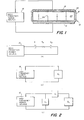
- FIG. 1 An electromagnetic discharge apparatus wherein high frequency power is capacitively coupled to the discharge is depicted in Figure 1 as a planar fluorescent light source in order to aid in understanding the principles of capacitive coupling to a low pressure discharge.
- the light source includes a discharge lamp 10, first conductor 12, and second conductor 14 and can include high frequency power source 16.
- Discharge lamp 10 includes lamp envelope 18 made of a light transmitting substance such as glass which encloses in interior region 20 a fill material which forms during discharge a plasma which emits ultraviolet radiation. Lamp 10 has no metal electrodes internal to lamp envelope 18 and no conductors passing through lamp envelope 18.
- Lamp envelope 18, shown in Figure 1 is generally planar in shape with two external surface regions which are parallel.
- the fill material typically includes at least one noble gas and mercury vapcr in equilibrium with a small droplet of mercury within envelope 18. Alternatively, a mercury-containing amalgam can be used in place of the mercury droplet.
- a thin phosphor coating 22 is applied to the inner surface of lamp envelope 18.
- First conductor 12 and second conductor 14 are located in close proximity to the first and second external surface regions, respectively, of lamp envelope 18. At least one of the conductors is optically transparent to permit light to exit from the apparatus.
- conductive wire mesh can be used as illustrated by first conductor 12 in Figure 1.
- the term "high frequency" refers to frequencies in the range from 10 MHz to 10 GHz.
- a preferred frequency range is the ISM band (industrial, scientific, and medical band) which ranges from 902 MHz to 928 MHz.
- One preferred frequency of operation is 915 MHz.
- Another preferred frequency is approximately 40 MHz.
- FIG. 2a A simplified equivalent circuit of discharge lamp 10 and conductors 12 and 14 is shown in Figure 2b wherein the series combination of R , C 1 , and C 2 is coupled to the output of high frequency power source 16. Since the plasma discharge in region 20 is conductive, its effective electrical impedance is represented by resistor Rp.
- C 1 represents the capacitance between first conductor 12 and the plasma in region 20 which is viewed as an electrode of C l .
- C 2 represents the capacitance between second conductor 14 and the plasma in region 20 which is viewed as an electrode of C 2 .
- Lamp envelope 18 is the dislectric material between the electrodes of both C 1 and C 2 .
- the representation herein of discharge lamps and associated conductors by an equivalent circuit including C 1 , C , and R is a simplified characterization of the actual apparatus. While the plasma is characterized as forming resistor R p and one electrode of each of capacitors C 1 and C 2 , the plasma'in fact is a gas which has a complex impedance and which is distributed throughout the lamp envelope. The plasma, there- fore, is not to be misunderstood as being a lumped, highly conductive capacitor electrode in the conventional sense.
- the reflection coefficient approaches zero and power is optimally delivered to the plasma discharge.
- high frequencies and large values of C 1 and C 2 are utilized.
- High values of C 1 and C 2 are obtained by using conductors 12 and 14 with large surface area.
- the value of C 1 and C 2 is also increased by decreasing the spacing between the electrodes of C 1 and C 2 , that is, by decreasing the thickness of lamp envelope 18.
- the impedances of C 1 and C 2 are, preferably, less than about 10% of the impedance of the plasma, R , at the operating frequency.
- any given light source configuration has an associated minimum frequency of operation below which power transfer becomes inefficient and matching components are necessary. This minimum frequency of operation varies with discharge lamp size and shape, conductor area, lamp envelope thickness, and lamp fill material. While the value of R depends on the fill material used, it has been found that when lamp envelope 18 contains neon at a pressure of a few torr with mercury present, the value of R p is approximately 50 ohms.
- the capacitive impedances of C 1 and C 2 are negligible at frequencies above about 500 MHz.
- a high frequency power source having a 50 ohm output impedance can efficiently deliver power to a plasma discharge without the use of additional matching elements when the operating frequency is above about 500 MHz.
- Virtually reflectionless discharges have been obtained at 915 MHz.
- circuit elements such as Z 1 and Z 2 as shown in Figure 2c can be used to accomplish matching between high frequency power source 16 having output impedance Z 0 and the discharge apparatus having impedance Z L .
- Such techniques for matching are well known L and described in P. M. Smith, Electronic Applications of the Smith Chart, pp. 115-128, McGraw-Hill, New York.
- Z 2 is coupled directly across the output of high frequency power source 16.
- Z is connected in series with load impedance Z L and the series combination of Z L and Z 1 is coupled directly across the output of high frequency power source 16.
- Z and Z 2 can be inductors or capacitors or combinations thereof with values depending on the frequen- c y of operation and the values of impedances Z 0 and Z L . Matching components are undesirable because of the increased cost and reduced reliability associated with their use.
- Capacitive coupling of high frequency power to low pressure discharges in lamps of the type described above can therefore be accomplished by performing the following steps.
- a first conductor 12 is positioned in close proximity to a first external surface region of discharge lamp 10 such that first conductor 12 and the plasma in region 20 act as a f.irst electrode pair, separated by lamp envelope 18, of a first capacitor C which is configured to have an impedance, at said high frequency, which is much less than the impedance R P of the plasma.
- a second conductor 14 is positioned in close proximity to a second external surfare region of discharge lamp 10 such that second conductor 14 and the plasma in region 20 act as a second electrode pair, separated by lamp envelope 18, of a second capacitor C 2 which is configured to have an impedance, at said high frequency, which is much less than the impedance R P of the plasma.
- the impedances of C 1 and C 2 at the frequency of operation are, preferably, less than about 10% of the plasma impedance R to avoid the necessity for matching components as described hereinabove.
- First conductor 12 and second conductor 14 are positioned so that, when a high frequency voltage is applied between conductors 12 and 14, inducing an electric field 24 therebetween, substantially all of electric field 24 is confined within discharge lamp 10.
- High frequency power is applied to first conductor 12 and second conductor 14 for inducing electric fields 24 in envelope 18 and causing discharge in the plasma. It has been found that capacitively coupled discharges operated in accordance with the above method tend toward uniformly distributed plasma within lamp envelope 18 and are, therefore, those which are optimal with respect to light generation.
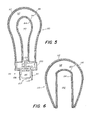
- An electromagnetic discharge apparatus is illustrated in Figure 3 as a compact fluorescent light source including discharge lamp 30, outer conductor 32, and inner conducto'- 34, and can include high frequency power source 35.
- Discharge lamp 30 includes lamp envelope 36 which has an outer surface which is generally pear-shaped and is similar in size and shape to commonly used incandescent lamps which are generally pear-shaped.
- Lamp envelope 36 includes a re-entrant cavity 38 which is generally cylin- drical in shape.
- a re-entrant cavity can be defined for the purposes of this disclosure as an open-ended cavity extending into a lamp envelope but not passing through the wall of the lamp.
- the re-entrant cavity is surrounded by the material of the lamp envelope except for the opening on the outer surface of the lamp envelope.
- the inner surface of the re-entrant cavity is external to the volume enclosed by the lamp envelope. While re-entrant cavity 38 is cylindrical in shape, re-entrant cavities, in general, can be of any shape.
- the fill material in interior region 40 forms during discharge a plasma which emits ultraviolet radiation.
- a small droplet of mercury with a noble gas (helium, neon, argon, kr pton, xenon) or mixtures of noble gases are typically used.
- Mercury-containing amalgams can be used in place of mercury.
- One preferred fill material is neon at a pressure of a few torr and about 3 milligrams of mercury.
- Lamp envelope 36 has on its inner surface a phosphor coating 42 which emits visible light upon absorption of ultraviolet light.
- Phosphors commonly used in commercially available fluorescent lamps are suitable for use in the present invention.
- One suitable phosphor is calcium halophosphate.
- known rare earth phosphors and blends thereof are preferred because of their ability to withstand the relatively high wall loading characteristic of the light source according to the present invention.
- Wall loading is the lamp power dissipation per unit area of light emitting surface.
- Inner conductor 34 can be solid or hollow and preferably fills re-entrant cavity 38. It has been found that the efficiency of the light source is increased if the surface of inner conductor 34 is polished to reflect light generated by discharge lamp 30 back into and through discharge lamp 30.
- Outer conductor 32 which is an optically transparent conductor such as metal mesh, substantially surrounds the outer surface of lamp envelope 36. In this discussion, the outer surface of lamp envelope 36 is defined as excluding the surface of re-entrant cavity 38.
- the plasma discharge is confined in a generally annular region 40 bounded by a relatively large diameter inner conductor 34 and an optically transparent outer conductor 32 which is generally coaxial with inner conductor 34.
- an electrical field running radially between outer conductor 32 and inner conductor 34 causes the gas t in region 40 to undergo electrical breakdown and subsequently a substantially steady plasma discharge forms throughout region 40.
- the discharge is a source of ultraviolet light, particularly at 254 nanometers.
- Phosphor coating 42 emits visible light upon absorption of ultraviolet light from the plasma discharge.
- phosphor coating 42 is omitted and envelope 36 is fabricated from material such as fused silica which is transparent to ultraviolet light.
- Inner conductor 34 is disposed in re-entrant cavity 38 such that inner conductor 34 and the plasma in region 40 act as a second electrode pair, separated by lamp envelope 36, of a second capacitor which is configured to have an impedance at the frequency of operation which is much less than the impedance of the plasma.
- the impedances of the first and second capacitors at the frequency of operation are preferably less than about 10% of the impedance of the plasma to avoid the necessity for matching components as described hereinabove.
- Conductors 32 and 34 are positioned so that when a high frequency voltage is applied between conductors 32 and 34, inducing an electric field therebetween, substantially all of the electric field is confined within discharge lamp 30.
- lamp envelopes of the present invention include a base region through which the re-entrant cavity passes and an enlarged region wherein the re-entrant cavity terminates and which has a larger cross-sectional area than the base region. These lamp envelopes are tapered inwardly from the enlarged region to the base region to form a continuous outer surface.
- the lamp envelope for example, can have an enlarged region which is generally spherical or can have an enlarged region which is generally cylindrical.
- a lamp envelope having an overall cylindrical outer shape is satisfactory, although less desirable.
- the crudely spherical shape of this lamp has an approximately isotropic radiation pattern similar to that of a frosted incandescent lamp.
- the replacement of an incandescent lamp by the apparatus of Figure 3 does not cause noticeable changes in illumination pattern.
- the equivalent light production of a standard 100 watt incandescent lamp is provided by the light source shown in Figure 3 with only 15 to 20 watts of high frequency power.
- the relatively easy starting conditions of the present lamp permit starting of the light source by the application of normal running power.
- an important feature of the present light source is that no starting circuits or other starting aids are required to initiate discharge.
- a compact fluorescent light source utilizing metallized electrodes is shown in Figure 4 and includes discharge lamp 50, outer conductor 52, and inner conductor 54 and can include high frequency power source 56.
- Discharge lamp 50 includes lamp envelope 58, which has an outer surface which is generally pear-shaped, and re-entrant cavity 60 which is generally cylindrical in shape.
- Lamp 50 also includes in interior region 62 a fill material which forms during discharge a plasma which emits ultraviolet radiation and has on its inner surface a phosphor coating 64 which emits visible light upon absorption of ultraviolet light.
- Outer conductor 52 which is an optically transparent conductor such as metal mesh, substantially surrounds the outer surface of lamp envelope 36 except for the surface of re-entrant cavity 60.
- Inner conductor 54 is a conductive coating disposed on the inner surface of re-entrant cavity 60 to form a metallized electrode. Electrical contact to inner conductor 54 is made by conductive resilient fingers 66 which are coupled to conductive member 68 which in turn is coupled to conductive member 70.
- Conductive member 72 is coupled to outer conductor 52.
- Conductive members 70 and 72 are also coupled to high frequency power source 56.
- Conductive members 68, 70, and 72 and resilient fingers 66 are operative to support discharge lamp 50 and to electrically couple outer conductor 52 and inner conductor 54 to high frequency power source 56. While the configuration shown in Figure 4 is satisfactory, numerous other coupling and lamp support arrangements can be used without departing from the scope of the present invention.
- Inner conductor 54 can be fabricated by any convenient metallization technique. Well known vacuum deposition techniques can be used. A layer of chrome is first applied to the inner surface of re-entrant cavity 60. Then a layer of conductive metal such as aluminum is applied over the chrome layer. Inner conductor 54 can also be formed by painting the inner surface of re-entrant cavity 60 with a conductive epoxy. It is preferred that inner conductor 54 have a light reflecting surface which is operative to reflect light emitted from discharge lamp 50 back to and through discharge lamp 50.
- Outer conductor 52 which is typically a conductive mesh, can alternatively be a conductive coating disposed on the outer surface of lamp envelope 58. The conductive coating is typically in a pattern which permits light to escape from the apparatus. 'One example is a grid pattern.
- Skin depth is a well known quantity which is related to the fact that high frequency power travels near the surface of a conductor rather than being uniformly distributed in the conductor. Skin depth is a measure of the depth to which high frequency power penetrates the conductor and decreases as the frequency of operation of the light source increases. Furthermore, when outer conductor 52 is substantially more than one skin depth in thickness, the light source is prevented from radiating power at high frequency.
- aluminum has a skin depth of about 3 microns for an operating frequency of 915 MHz.
- an inner conductor 54 of at least 10 microns thickness results in a substantially field-free re-entrant cavity 60 at 915 MHz and an outer conductor 52 of at least 10 microns thickness prevents radiation of 915 MHz power.
- thicker conductors are required to achieve effective shielding.
- a preferred embodiment of a compact fluorescent light source wherein the inner conductor is a conductive coating disposed on the lamp envelope is depicted in Figure 5.
- the light source includes discharge lamp 80, outer conductor 82, and immer conductor 84 and can include high fre- ⁇ quency power source 86.
- Discharge lamp 80 includes lamp envelope 88, which has an outer surface which is generally pear-shaped, and re-entrant cavity 90 which has substantially the same shape as the outer surface of envelope 88.
- Lamp 80 also includes in interior region 92 a fill material which forms during discharge a plasma which emits ultraviolet radiation and has on its inner surface a phosphor coating 94 which emits visible light upon absorption of ultraviolet light.
- Outer conductor 82 which is an optically transparent conductor such as metal mesh, substantially surrounds the outer surface of lamp envelope 88 except for the surface off re-entrar' cavity 90.
- Inner conductor 84 is a conductive coaling disposed on the inner surface of re-entrant cavity 90 to form a metallized electrode.
- the discussion hereinab0ove of application techniques and thickness of conductor 54 in Figure 4 is applicable to inner conductor 84.
- the use of a metallized electrode permits inner conductor 82 to follow the contours of re-entrant cavity 90.
- re-entrant cavity 90 has the same general shape as the outer surface of lamp envelope 88, the spacing between outer conductor 82 and inner conductor 84 is generally uniform and a more uniform light output results for reasons stated hereinafter.
- the use in re-entrant cavity 90 of solid or hollow electrodes which have the shape of re-entrant cavity 90 is impractical because of the problem of positioning such an electrode in cavity 90.
- the shape of the re-entrant cavity can be made to correspond with the outer shape of the lamp envelope thus insuring a more or less uniform spacing between inner and outer conductors.
- Outer conductor 82 alternatively can be a conductive coating disposed on the outer surface of envelope 88 in a pattern, as described hereinabove.
- electrodes formed as metallic coatings on the surface of lamp envelope 88 have the following advantages: (1) The use of a substantially pear-shaped inner electrode, made possible by metallization, results in uniform self-trapping of 254 nm radiation in the mercury vapor and reduced self-trapping or imprisonment of this radiation in the largest diameter, globular portion of the lamp. The result is increased light output and a more uniformly activated phosphor surface. (2) The increased surface area and inherently close proximity of the metallized surface to the ervelope material, ensures increased and maximized capacitance between the metallization and the plasma. This results in improved coupling at all frequencies and a lowering of the minimum frequency which may be used effectively.
- the metallized surface facing the plasma discharge will typically present a highly reflecting, nearly mirror quality, surface to visible light propagating inward toward the re-entrant cavity. This results in improved light output, contributing to the isotropic visible radiation from the lamp. Moreover, the metallized surface facing the discharge is permanently protected from oxidation or other chemical attack and so retains its mirror quality.
- the metallized electrode has extremely small mass, a factor which contributes to the ruggedness of this lamp over filamented lamps or lamps in the prior art which contain massive coils or magnetic material.
- the metallized electrode leaves a field-free cavity 90 within the lamp which can, where needed, contain circuit components or other articles necessary to the lamp's operation.
- the metallized electrode is permanently bonded to the glass or other envelope material thereby providing automatic disconnection of the high frequency source when envelope 88 is removed or broken.
- high frequency power source 86 is located in lamp base 94 which includes screw-in base 96 and conductive member 100.
- Base 96 can be the type commonly used on incandescent lamps for connection to 115 volts ac 60 Hz household power and commonly known as an Edison screw base.
- High frequency power source 86 which is coupled to the conductors of base 96 by conductors 102 and 106, receives 110 volts ac 60 Hz power through base 96 and generates high frequency output power which is coupled to inner conductor 84 through resilient conductive fingers 104.
- Outer conductor 82 is coupled to ground through conductive member 100 and base 96.
- discharge lamp 80 has a resistive impedance of approximately 50 ohms as discussed hereinabove, various well known high frequency, solid state power sources can be used to power the light source. Since high frequency power source 86 is incorporated into lamp base 94, the light source can be used as a screw-in replacement for an incandescent lamp.
- discharge lamp 80, outer conductor 82 and inner conductor 84 can be utilized in conjunction with a remote high frequency power supply as illustrated in Figure 4. Furthermore, the configuration of power source and lamp base shown in Figure 5 can be utilized in the light ources shown in Figures 3 and 4.
- FIG. 6 A preferred embodiment of a compact fluorescent light source which can be operated at lower frequencies is illustrated in Figure 6.
- the light source includes discharge lamp 110, outer conductor 112, and inner conductor 114.
- Discharge lamp 110 can be supported and electrically coupled to a high frequency power source as shown in Figure 4 or as shown in Figure 5 or by other configurations which will be obvious to those skilled in the art.
- Lamp 110 includes lamp envelope 116 which has in interior region 118 a fill material which forms during discharge a plasma which emits ultraviolet radiation and has on its inner surface a phosphor coating 120 which emits visible light upon absorption of ultraviolet light.
- the discussion hereinabove of discharge lamp 30 with respect to variations of lamp shapes, advantages of the disclosed lamp shapes, capacitive coupling techniques, and suitable fill materials and phosphor coatings is applicable to discharge lamp 110.
- Lamp envelope 116 has a larger diameter and therefore a larger outer surface area than envelope 36 in Figure 3.
- outer conductor 112 which surrounds the outer surface of discharge lamp 110, also has a greater surface area than outer conductor 32 in Figure 3.
- lamp envelope 116 has a re-entrant cavity 122 of substantially larger diameter and therefore larger surface area than re-entrant cavity 38 in Figure 3.
- inner conductor 114 which is a conductive coating disposed on the inner surface of re-entrant cavity 1.22, has a larger surface area than inner conductor 34 in Figure 3.
- Outer conductor 112 is optically transparent, for example a metal mesh, while inner conductor 114 can be formed according to the techniques discussed hereinabove in connection with conductor 54 in Figure 4.
- Outer conductor 112 alternatively can be a conductive coating disposed on the outer surface of envelope 116 in a pattern, as described hereinabove.
- the large surface areas of inner conductor 114 and outer conductor 112 provide a substantial increase in coupling capacitance which is desirable at the lower end of the usable frequency range as discussed hereinabove.
- Discharge lamp 110 having increased coupling capacitance can also be utilized in a light source wherein the inner conductor is a solid or hollow conductor rather than a conductive coating.
- the light sources shown in Figures 4-6 include a discharge lamp as above described, an inner conductor and an outer conductor.
- the outer conductor is disposed around the outer surface of the lamp envelope such that the outer conductor and the plasma act as a first electrode pair, separated by the lamp envelope, of a first capacitor which is configured to have an impedance at the frequency of operation which is much less than the impedance of the plasma.
- the inner conductor is a conductive coating disposed on the inner surface of the re-entrant cavity such that the inner conductor and the plasma act as a second electrode pair, separated by the lamp envelope, of a second capacitor which is configured to have an impedance at the frequency of operation which is much less than the impedance of the plasma.
- the impedance of the first and second capacitors at the frequency of operation are preferably less than 10% of the plasma impedance to avoid the necessity for matching components as described hereinabove.
- the inner and outer conductors are adapted for receiving high frequency power and are positioned so that when a high frequency voltage is applied between the inner and outer conductors, inducing an electric field therebetween, substantially all of the electric field is confined within the discharge lamp.
- High frequency power source 16 in Figures 1 and 2, power source 35 in Figure 3, power source 56 in Figure 4, and power source 86 in Figure 5 can be any suitable high frequency power source capable of supplying the required power level at the operating frequency of the light source.
- the high frequency power sources used herein convert dc or low frequency ac power to high frequency power in the 10 MHz to 10 GHz range.
- the light source disclosed herein which has a light output equivalent to a 100 watt incandescent lamp requires 20 watts at 915 MHz with a 50 ohm source impedance.
- the most common input power is 60 Hz, 115 volt ac household power.
- the high frequency power sources used herein can be made to operate from 50 Hz, 400 Hz, or three-phase inputs. Also, the input voltage level is a matter of design choice.
- One suitable power source is shown in U. S. Patent No. 4,070,603 issued January 24, 1978 to Regan et al. When this power source is used in the incandescent replacement light source shown in Figure 5, a dc power source is added to convert the 60 Hz input to dc.
- Tubulations used for introduction of phosphor coating materials and lamp fill materials into the discharge lamp, are not shown in Figures 1 and 3-6. However, these may be located at various points on the lamp envelope depending on preferred manufacturing technique.
- Light sources constructed as herein disclosed provide, with an input high frequency power of only 15 to 20 watts, . light output equal to or greater than that produced by a 100 watt incandescent lamp. Whereas inductively coupled electrodeless fluorescent light sources have claimed outputs of 80 lumens per watt of high frequency input power, the light sources herein disclosed have outputs in the range of 100 lumens per watt of high frequency input power. Further testing reveals that this light source operates with a useful life of at least 5000 hours. Other tests have shown that the light source disclosed herein starts and hot starts reliably, that it is unaffected by orientation, and that its low surface temperature is within a safe range in the event of personal contact. Furthermore, the light output can be dimmed over a wide range by varying the input high frequency power level. Thus, it is seen that the light source disclosed herein provides energy efficiency, elimination of massive coils and magnetic material, a uniform light output, long operating life, and ruggedness.
Applications Claiming Priority (2)
| Application Number | Priority Date | Filing Date | Title |
|---|---|---|---|
| US92914 | 1979-11-09 | ||
| US06/092,914 US4266166A (en) | 1979-11-09 | 1979-11-09 | Compact fluorescent light source having metallized electrodes |
Publications (3)
| Publication Number | Publication Date |
|---|---|
| EP0029896A2 true EP0029896A2 (de) | 1981-06-10 |
| EP0029896A3 EP0029896A3 (en) | 1981-08-26 |
| EP0029896B1 EP0029896B1 (de) | 1985-01-30 |
Family
ID=22235773
Family Applications (1)
| Application Number | Title | Priority Date | Filing Date |
|---|---|---|---|
| EP80106189A Expired EP0029896B1 (de) | 1979-11-09 | 1980-10-10 | Kompakte fluoreszierende Lichtquelle mit metallisierten Elektroden |
Country Status (5)
| Country | Link |
|---|---|
| US (1) | US4266166A (de) |
| EP (1) | EP0029896B1 (de) |
| JP (1) | JPS56128567A (de) |
| CA (1) | CA1149078A (de) |
| DE (1) | DE3070071D1 (de) |
Cited By (2)
| Publication number | Priority date | Publication date | Assignee | Title |
|---|---|---|---|---|
| GB2133612A (en) * | 1982-12-29 | 1984-07-25 | Philips Nv | Gas and/or vapour discharge lamp |
| WO1987003161A1 (en) * | 1985-11-07 | 1987-05-21 | Mattson, Bengt | A lamp assembly |
Families Citing this family (21)
| Publication number | Priority date | Publication date | Assignee | Title |
|---|---|---|---|---|
| US4427925A (en) | 1981-11-18 | 1984-01-24 | Gte Laboratories Incorporated | Electromagnetic discharge apparatus |
| US5173638A (en) * | 1986-07-22 | 1992-12-22 | Bbc Brown, Boveri Ag | High-power radiator |
| CH670171A5 (de) * | 1986-07-22 | 1989-05-12 | Bbc Brown Boveri & Cie | |
| CH675178A5 (de) * | 1987-10-23 | 1990-08-31 | Bbc Brown Boveri & Cie | |
| JPH01243364A (ja) * | 1988-03-25 | 1989-09-28 | Matsushita Electric Works Ltd | 無電極放電灯装置 |
| US4968142A (en) * | 1989-06-02 | 1990-11-06 | The United States Of America As Represented By The United States Department Of Energy | Closed inductively coupled plasma cell |
| US5013976A (en) * | 1989-12-26 | 1991-05-07 | Gte Products Corporation | Electrodeless glow discharge lamp |
| US5113121A (en) * | 1990-05-15 | 1992-05-12 | Gte Laboratories Incorporated | Electrodeless HID lamp with lamp capsule |
| US5070277A (en) * | 1990-05-15 | 1991-12-03 | Gte Laboratories Incorporated | Electrodless hid lamp with microwave power coupler |
| US5220236A (en) * | 1991-02-01 | 1993-06-15 | Hughes Aircraft Company | Geometry enhanced optical output for rf excited fluorescent lights |
| DE59105798D1 (de) * | 1991-04-15 | 1995-07-27 | Heraeus Noblelight Gmbh | Bestrahlungseinrichtung. |
| US5146140A (en) * | 1991-06-18 | 1992-09-08 | Gte Products Corporation | Method and apparatus to reduce Hg loss in rf capacitively coupled gas discharges |
| US5397966A (en) * | 1992-05-20 | 1995-03-14 | Diablo Research Corporation | Radio frequency interference reduction arrangements for electrodeless discharge lamps |
| US5619103A (en) * | 1993-11-02 | 1997-04-08 | Wisconsin Alumni Research Foundation | Inductively coupled plasma generating devices |
| US5523655A (en) * | 1994-08-31 | 1996-06-04 | Osram Sylvania Inc. | Neon fluorescent lamp and method of operating |
| CA2325625A1 (en) * | 1998-03-24 | 1999-09-30 | Corning Incorporated | External electrode driven discharge lamp |
| US6522085B2 (en) * | 2001-07-16 | 2003-02-18 | Matsushita Research And Development Laboratories Inc | High light output electrodeless fluorescent closed-loop lamp |
| US7298091B2 (en) * | 2002-02-01 | 2007-11-20 | The Regents Of The University Of California | Matching network for RF plasma source |
| US7309732B1 (en) * | 2003-04-21 | 2007-12-18 | Henkel Corporation | UV and UV/moisture dual curable compositions with improved cure through volume |
| TW200913001A (en) * | 2007-08-03 | 2009-03-16 | Orc Mfg Co Ltd | Discharge lamp |
| DE202008008731U1 (de) * | 2008-07-02 | 2009-11-19 | Melitta Haushaltsprodukte Gmbh & Co. Kg | Anordnung zur Herstellung von Plasma |
Citations (1)
| Publication number | Priority date | Publication date | Assignee | Title |
|---|---|---|---|---|
| US4010400A (en) * | 1975-08-13 | 1977-03-01 | Hollister Donald D | Light generation by an electrodeless fluorescent lamp |
Family Cites Families (6)
| Publication number | Priority date | Publication date | Assignee | Title |
|---|---|---|---|---|
| US4002944A (en) * | 1975-04-21 | 1977-01-11 | Gte Laboratories Incorporated | Internal match starter for termination fixture lamps |
| US3943403A (en) * | 1975-04-21 | 1976-03-09 | Gte Laboratories Incorporated | Electrodeless light source utilizing a lamp termination fixture having parallel capacitive impedance matching capability |
| US3942068A (en) * | 1975-04-21 | 1976-03-02 | Gte Laboratories Incorporated | Electrodeless light source with a termination fixture having an improved center conductor for arc shaping capability |
| US4063132A (en) * | 1976-08-04 | 1977-12-13 | Gte Laboratories Inc. | DC powered microwave discharge in an electrodeless light source |
| US4185228A (en) * | 1978-10-19 | 1980-01-22 | Gte Laboratories Incorporated | Electrodeless light source with self-contained excitation source |
| JPS55156049A (en) * | 1979-05-22 | 1980-12-04 | Aron Kasei Kk | Grain floor arranging material |
-
1979
- 1979-11-09 US US06/092,914 patent/US4266166A/en not_active Expired - Lifetime
-
1980
- 1980-10-10 EP EP80106189A patent/EP0029896B1/de not_active Expired
- 1980-10-10 DE DE8080106189T patent/DE3070071D1/de not_active Expired
- 1980-10-30 CA CA000363585A patent/CA1149078A/en not_active Expired
- 1980-11-07 JP JP15604880A patent/JPS56128567A/ja active Pending
Patent Citations (2)
| Publication number | Priority date | Publication date | Assignee | Title |
|---|---|---|---|---|
| US4010400A (en) * | 1975-08-13 | 1977-03-01 | Hollister Donald D | Light generation by an electrodeless fluorescent lamp |
| US4119889A (en) * | 1975-08-13 | 1978-10-10 | Hollister Donald D | Method and means for improving the efficiency of light generation by an electrodeless fluorescent lamp |
Cited By (2)
| Publication number | Priority date | Publication date | Assignee | Title |
|---|---|---|---|---|
| GB2133612A (en) * | 1982-12-29 | 1984-07-25 | Philips Nv | Gas and/or vapour discharge lamp |
| WO1987003161A1 (en) * | 1985-11-07 | 1987-05-21 | Mattson, Bengt | A lamp assembly |
Also Published As
| Publication number | Publication date |
|---|---|
| CA1149078A (en) | 1983-06-28 |
| JPS56128567A (en) | 1981-10-08 |
| US4266166A (en) | 1981-05-05 |
| EP0029896A3 (en) | 1981-08-26 |
| EP0029896B1 (de) | 1985-01-30 |
| DE3070071D1 (en) | 1985-03-14 |
Similar Documents
| Publication | Publication Date | Title |
|---|---|---|
| US4266167A (en) | Compact fluorescent light source and method of excitation thereof | |
| US4266166A (en) | Compact fluorescent light source having metallized electrodes | |
| US5325024A (en) | Light source including parallel driven low pressure RF fluorescent lamps | |
| CA2108434C (en) | Capacitively coupled rf fluorescent lamp with rf magnetic enhancement | |
| US4189661A (en) | Electrodeless fluorescent light source | |
| US4710678A (en) | Electrodeless low-pressure discharge lamp | |
| US6768248B2 (en) | Electrodeless lamp | |
| US4727295A (en) | Electrodeless low-pressure discharge lamp | |
| EP0698914A1 (de) | Elektrodenlose Entladungslampe | |
| US5289085A (en) | Capacitively driven RF light source having notched electrode for improved starting | |
| US20070138927A1 (en) | Electrodeless gas discharge lamp | |
| US5013976A (en) | Electrodeless glow discharge lamp | |
| US8860323B2 (en) | Plasma lamp with lumped components | |
| US4187447A (en) | Electrodeless fluorescent lamp with reduced spurious electromagnetic radiation | |
| US5773926A (en) | Electrodeless fluorescent lamp with cold spot control | |
| US3997816A (en) | Starting assist device for an electrodeless light source | |
| US8525430B2 (en) | Helical structure and method for plasma lamp | |
| EP0593312B1 (de) | Fluoreszierende Lichtquelle | |
| US6710535B2 (en) | Low-pressure gas discharge lamps | |
| US6507151B1 (en) | Gas discharge lamp with a capactive excitation structure | |
| CA2185267C (en) | High intensity electrodeless low pressure light source | |
| US8102107B2 (en) | Light-emitting devices having excited sulfur medium by inductively-coupled electrons | |
| KR800001141B1 (ko) | 무전극 방전 램프 | |
| JPH09231949A (ja) | 無電極低圧放電ランプ | |
| JPH08287877A (ja) | 無電極放電ランプ |
Legal Events
| Date | Code | Title | Description |
|---|---|---|---|
| PUAI | Public reference made under article 153(3) epc to a published international application that has entered the european phase |
Free format text: ORIGINAL CODE: 0009012 |
|
| 17P | Request for examination filed |
Effective date: 19801010 |
|
| AK | Designated contracting states |
Designated state(s): DE FR GB NL |
|
| PUAL | Search report despatched |
Free format text: ORIGINAL CODE: 0009013 |
|
| AK | Designated contracting states |
Designated state(s): DE FR GB NL |
|
| GRAA | (expected) grant |
Free format text: ORIGINAL CODE: 0009210 |
|
| AK | Designated contracting states |
Designated state(s): DE FR GB NL |
|
| REF | Corresponds to: |
Ref document number: 3070071 Country of ref document: DE Date of ref document: 19850314 |
|
| ET | Fr: translation filed | ||
| PLBE | No opposition filed within time limit |
Free format text: ORIGINAL CODE: 0009261 |
|
| STAA | Information on the status of an ep patent application or granted ep patent |
Free format text: STATUS: NO OPPOSITION FILED WITHIN TIME LIMIT |
|
| 26N | No opposition filed | ||
| PGFP | Annual fee paid to national office [announced via postgrant information from national office to epo] |
Ref country code: GB Payment date: 19890930 Year of fee payment: 10 |
|
| PGFP | Annual fee paid to national office [announced via postgrant information from national office to epo] |
Ref country code: FR Payment date: 19891013 Year of fee payment: 10 |
|
| PGFP | Annual fee paid to national office [announced via postgrant information from national office to epo] |
Ref country code: NL Payment date: 19891031 Year of fee payment: 10 |
|
| PGFP | Annual fee paid to national office [announced via postgrant information from national office to epo] |
Ref country code: DE Payment date: 19891130 Year of fee payment: 10 |
|
| PG25 | Lapsed in a contracting state [announced via postgrant information from national office to epo] |
Ref country code: GB Effective date: 19901010 |
|
| PG25 | Lapsed in a contracting state [announced via postgrant information from national office to epo] |
Ref country code: NL Effective date: 19910501 |
|
| GBPC | Gb: european patent ceased through non-payment of renewal fee | ||
| NLV4 | Nl: lapsed or anulled due to non-payment of the annual fee | ||
| PG25 | Lapsed in a contracting state [announced via postgrant information from national office to epo] |
Ref country code: FR Effective date: 19910628 |
|
| PG25 | Lapsed in a contracting state [announced via postgrant information from national office to epo] |
Ref country code: DE Effective date: 19910702 |
|
| REG | Reference to a national code |
Ref country code: FR Ref legal event code: ST |