EP0029744B1 - Solar powered automatic turn-on control unit - Google Patents
Solar powered automatic turn-on control unit Download PDFInfo
- Publication number
- EP0029744B1 EP0029744B1 EP19800304238 EP80304238A EP0029744B1 EP 0029744 B1 EP0029744 B1 EP 0029744B1 EP 19800304238 EP19800304238 EP 19800304238 EP 80304238 A EP80304238 A EP 80304238A EP 0029744 B1 EP0029744 B1 EP 0029744B1
- Authority
- EP
- European Patent Office
- Prior art keywords
- power
- load
- solar
- source
- panel
- Prior art date
- Legal status (The legal status is an assumption and is not a legal conclusion. Google has not performed a legal analysis and makes no representation as to the accuracy of the status listed.)
- Expired
Links
- 230000004044 response Effects 0.000 claims description 34
- 230000008878 coupling Effects 0.000 claims description 12
- 238000010168 coupling process Methods 0.000 claims description 12
- 238000005859 coupling reaction Methods 0.000 claims description 12
- 238000000034 method Methods 0.000 claims description 2
- 230000000694 effects Effects 0.000 description 7
- 230000001276 controlling effect Effects 0.000 description 4
- 230000007423 decrease Effects 0.000 description 4
- 238000010586 diagram Methods 0.000 description 4
- 235000014676 Phragmites communis Nutrition 0.000 description 3
- 238000004804 winding Methods 0.000 description 3
- 230000008859 change Effects 0.000 description 2
- 230000001965 increasing effect Effects 0.000 description 2
- 230000000670 limiting effect Effects 0.000 description 2
- 238000012544 monitoring process Methods 0.000 description 2
- 230000005855 radiation Effects 0.000 description 2
- 230000001105 regulatory effect Effects 0.000 description 2
- 230000001360 synchronised effect Effects 0.000 description 2
- 230000001052 transient effect Effects 0.000 description 2
- XUIMIQQOPSSXEZ-UHFFFAOYSA-N Silicon Chemical compound [Si] XUIMIQQOPSSXEZ-UHFFFAOYSA-N 0.000 description 1
- 230000002411 adverse Effects 0.000 description 1
- 230000003247 decreasing effect Effects 0.000 description 1
- 230000005672 electromagnetic field Effects 0.000 description 1
- 238000004146 energy storage Methods 0.000 description 1
- 230000001939 inductive effect Effects 0.000 description 1
- 230000000422 nocturnal effect Effects 0.000 description 1
- 230000002829 reductive effect Effects 0.000 description 1
- 230000002441 reversible effect Effects 0.000 description 1
- 229910052710 silicon Inorganic materials 0.000 description 1
- 239000010703 silicon Substances 0.000 description 1
- 230000007704 transition Effects 0.000 description 1
Images

Classifications
-
- G—PHYSICS
- G05—CONTROLLING; REGULATING
- G05F—SYSTEMS FOR REGULATING ELECTRIC OR MAGNETIC VARIABLES
- G05F1/00—Automatic systems in which deviations of an electric quantity from one or more predetermined values are detected at the output of the system and fed back to a device within the system to restore the detected quantity to its predetermined value or values, i.e. retroactive systems
- G05F1/66—Regulating electric power
- G05F1/67—Regulating electric power to the maximum power available from a generator, e.g. from solar cell
-
- Y—GENERAL TAGGING OF NEW TECHNOLOGICAL DEVELOPMENTS; GENERAL TAGGING OF CROSS-SECTIONAL TECHNOLOGIES SPANNING OVER SEVERAL SECTIONS OF THE IPC; TECHNICAL SUBJECTS COVERED BY FORMER USPC CROSS-REFERENCE ART COLLECTIONS [XRACs] AND DIGESTS
- Y02—TECHNOLOGIES OR APPLICATIONS FOR MITIGATION OR ADAPTATION AGAINST CLIMATE CHANGE
- Y02E—REDUCTION OF GREENHOUSE GAS [GHG] EMISSIONS, RELATED TO ENERGY GENERATION, TRANSMISSION OR DISTRIBUTION
- Y02E10/00—Energy generation through renewable energy sources
- Y02E10/50—Photovoltaic [PV] energy
- Y02E10/56—Power conversion systems, e.g. maximum power point trackers
-
- Y—GENERAL TAGGING OF NEW TECHNOLOGICAL DEVELOPMENTS; GENERAL TAGGING OF CROSS-SECTIONAL TECHNOLOGIES SPANNING OVER SEVERAL SECTIONS OF THE IPC; TECHNICAL SUBJECTS COVERED BY FORMER USPC CROSS-REFERENCE ART COLLECTIONS [XRACs] AND DIGESTS
- Y10—TECHNICAL SUBJECTS COVERED BY FORMER USPC
- Y10S—TECHNICAL SUBJECTS COVERED BY FORMER USPC CROSS-REFERENCE ART COLLECTIONS [XRACs] AND DIGESTS
- Y10S136/00—Batteries: thermoelectric and photoelectric
- Y10S136/291—Applications
- Y10S136/293—Circuits
-
- Y—GENERAL TAGGING OF NEW TECHNOLOGICAL DEVELOPMENTS; GENERAL TAGGING OF CROSS-SECTIONAL TECHNOLOGIES SPANNING OVER SEVERAL SECTIONS OF THE IPC; TECHNICAL SUBJECTS COVERED BY FORMER USPC CROSS-REFERENCE ART COLLECTIONS [XRACs] AND DIGESTS
- Y10—TECHNICAL SUBJECTS COVERED BY FORMER USPC
- Y10S—TECHNICAL SUBJECTS COVERED BY FORMER USPC CROSS-REFERENCE ART COLLECTIONS [XRACs] AND DIGESTS
- Y10S323/00—Electricity: power supply or regulation systems
- Y10S323/906—Solar cell systems
Definitions
- the present invention relates generally to a system and circuit for controlling the power applied by a photovoltaic solar panel d.c. source to a load, and, in preferred embodiments of the invention, to such a system and circuit wherein a series switch between the panel and the load is selectively opened and closed in response to the voltage level derived from the panel.
- the voltage derived from a photovoltaic solar panel d.c. source is a function of the sunlight incident on the panel and the temperature of the panel. Therefore, the voltage derived from the panel is highly variable due to the long and short term variations of solar energy incident on the panel.
- the available power per unit area of the solar panel goes from a nocturnal value of zero to a maximum value at the middle of a sunny day.
- the power derived from the panel may have a relatively constant value during the entire daytime hours on hazy days.
- the power derived from the panel can also have sudden variations due to clouds transiently in the field of view of the panel to the sun.
- Solar panel systems are presently being designed wherein a load is driven directly by the panel output voltage without the intermediary of an energy storage device, such as a rechargeable battery.
- Such systems usually include, for efficient operation, a chopping d.c. to a.c. inverter, with associated control circuitry.
- a chopping d.c. to a.c. inverter with associated control circuitry.
- One particularly advantageous chopper is disclosed in U.S. Patent 4,135,235, wherein a pseudo-sinusoidal, notched, multilevel waveform is derived from a d.c. source and supplied to an a.c load, such as a synchronous motor.
- This inverter preferably controlled by a variable frequency function generator as disclosed in U.S. Patent 4,167,775, is such that the power output and current supplied from the d.c.
- the source to the a.c. load increase proportionately with fundamental chopping frequency of the inverter. It is desired to supply maximum power from the panel to the inverter and to a load. However, the maximum power which can be derived from the panel is variable, as indicated above.
- the output power of the panel is a function of the panel load, which in turn controls the panel output voltage and current.
- the output of a photovoltaic solar panel can thus be represented as a family of curves for the panel voltage versus current output parameters.
- the open circuit voltage and short circuit current of each curve in the family both increases when the level of the incident solar energy on a panel increases for a given temperature.
- Each of the curves has a point corresponding to maximum power, at which the curve has a slope of minus one.
- Each of the curves has slopes with absolute values greater than one and less than one for currents respectively greater than and less than the maximum power point.
- Equipment to track the maximum available power from the panel and to control the chopping frequency of the inverter in response thereto must be shut down in an orderly fashion when the available power from the solar panel is reduced below some minimum value necessary to maintain control of the inverter. Also, in day-night ar " ; night-day transitions, it is necessary to remove power from the inverter and control circuitry and supply power to the control circuitry and inverter in an orderly manner, while always ensuring that sufficient control power exists to meet stability requirements of the inverter and the load.
- U.S. Patent 3,488,575 there is disclosed a solar energy system having a switch arranged in circuit between the solar cell and its load for disconnecting the cell from the load in the absence of sufficient light falling on the cell.
- the switch is a reed switch having a winding which is energised by the output voltage of the solar cell. Providing the cell output voltage exceeds a given level, the electromagnetic field generated by the winding is sufficient to hold the reed switch closed.
- the winding is permanently energised and so is always consuming energy produced by the solar cell which is wasteful.
- opening and closing of the reed switch takes place at a given solar cell output voltage so that if the cell output fluctuates at around the threshold level, the cell will be successively connected and disconnected to the load which is disadvantageous.
- French Patent 2,175,653 discloses a fairly complex control circuit which connects part of the cell output to a storage battery when the cell output power exceeds the power requirement of the load, but, when the cell output falls below that required by the load, the cell is disconnected from the battery and the battery re-connected to the load to boost the power supplied to it from the cell.
- the system uses a mode detector whose function is to control operation of the required switching as between the solar cell, battery and load according to a comparison between the cell output power and the power requirement of the load.
- the mode detector has a controllable hysteresis range. Therefore, small fluctuations in solar cell output power around the lower power requirement and within the hysteresis range will not result in the circuitry continually switching one way and then the other.
- the hysteresis effect displayed by the mode detector is an in-built design characteristic of the mode detector itself.
- a solar energy system comprising a photovoltaic solar DC source; a load; control circuitry, including a maximum power point tracker, arranged to transfer the output power of the solar source to the load such that the solar DC source is maintained operating substantially at the point corresponding to maximum power on its output voltage-versus-current characteristic, characterised by a turn-on circuit between the output of the solar source and the input to the control circuitry, said turn-on circuit being arranged to provide no output when an output parameter of the solar source is below a predetermined threshold level but to turn-on, to feed the output of the solar source through to the load via the control circuitry, when said predetermined threshold level is exceeded, the turn-on circuit comprising a first series switch between the solar source and said control circuitry, for selectively supplying voltage having one level to the load, a dummy load arranged in a branch circuit in shunt with the solar source, said branch circuit including a switch in said branch circuit, such that while said output parameter of said solar source is below
- a method of controlling the application of d.c output power of a photovoltaic solar source to a load comprising comparing an output parameter of the solar source with a predetermined threshold level, selectively controlling the coupling of power from the solar source either through a dummy load arranged in a branch circuit in shunt with the solar source or through the load itself according to the comparison result, such that while the output parameter of said source is below said predetermined level, the source power is coupled through the dummy load to be dissipated therein and no power is available for coupling through to the load, but while said predetermined value is exceeded, the source power is coupled through to the load whereby the power dissipated in the dummy load is now available for supply to the load, the coupling of power through to the load being via control circuitry, including a maximum power point tracker, such that the source power, when coupled through to the load, is controlled so as to maintain the solar source operating substantially at the point corresponding to maximum power on its
- this solar energy system due to the particular shape that the output voltage-versus-current characteristics of the solar energy system has, will operate with a hysteresis effect, without the need for any special in-built circuit elements for achieving this result.
- Embodiments of the present invention provide a new and improved circuit and system for providing orderly control of the power applied by a photovoltaic solar panel d.c. source to a load despite varying long and short term solar conditions of the panel.
- Such embodiments may include an inverter in the control circuitry which transfers the output power of the solar energy source to the load, the inverter having a chopping frequency controlled so that maximum available power from the panel is supplied to the inverter and orderly control for the turn-on and turn-off of the inverter and control circuitry thereof is provided.
- a system for providing orderly control of the power applied by a photovoltaic solar panel d.c. source to a load comprises means for coupling power from the panel to an inverter that drives the load and for preventing the coupling of power from the panel to the inverter in response to the voltage level of the panel being respectively greater than a predetermined value and less than a predetermined value.
- the coupling means is utilised in combination with an inverter control circuit that is responsive to the voltage from the source to control the switching frequency of the inverter so that substantially maximum power is supplied by the panel to the inverter for the incident solar energy and temperature of the panel.
- the inverter control circuit requires appreciably less power than the load and includes an input power supply terminal that is selectively connected to the output of the photovoltaic solar panel d.c. source.
- the control circuit power supply terminal is selectively connected to the panel so that power is coupled to the terminal or decoupled from the terminal depending upon the voltage derived from the panel.
- the coupling of power to the inverter and the control circuitry is provided with voltage hysteresis.
- the panel voltage in order to change the state of a switch that couples power from the panel to the inverter and a second switch which couples power from the panel to the control circuitry, the panel voltage must drop below a level that initially causes the switches to be activated into a conducting state.
- the hysteresis is provided by a pair of dummy loads that are connected in a shunt with the panel only while the switches are in a cut-off condition.
- While the dummy loads are connected in shunt with panels, they reduce the output voltage of the panel until the panel is responsive to a predetermined level of solar energy at a particular temperature.
- the switches are activated and the dummy loads are disconnected from the panel. Thereby, power is available from the panel which can be applied to the inverter and an actual load, rather than to the dummy loads.
- Disconnecting the dummy loads from the panel enables the panel voltage to increase above a threshold value at which the switches connected to the inverter and the inverter control circuitry are activated to a closed condition. These switches are not returned to an open circuit condition until the panel voltage drops below the threshold value.
- the panel is loaded with an impedance that causes the panel to derive the output parameter with a value different from the parameter value at the maximum power point for the panel at the threshold while the panel is decoupled from the load.
- the panel is coupled to the load while the panel is operated substantially at the maximum power.
- the hysteresis effect relies upon the family of curves for the voltage versus current output parameters of the panels.
- the power supplied by the panel to the load is controlled by monitoring one of the output parameters (voltage or current) of the panel to indicate whether the solar energy incident on the panel is above or below a reference value.
- the parameter is the output voltage of the panel, although it is to be understood that the output current of the panel can also be monitored.
- the reference value is proportional to the panel d.c. output voltage.
- the dummy load In response to the parameter indicating that the incident energy is below the threshold, the dummy load is connected to the panel, and the series switch between the panel and the load is open circuited, to prevent the coupling .power from the panel to the load:
- the dummy load causes the panel to operate along the portion of the curve having a slope greater than one. If, however, current is monitored, the dummy load causes the panel to operate along the portion of the curve where the slope of the curve is less than one. In any event, the dummy load causes the output power of the panel to differ from the panel maximum power at the threshold value of the incident energy. In response to the parameter indicating that the incident energy is above the threshold, the dummy load is disconnected from the panel.
- a silicon photovoltaic solar panel 11 is illustrated as including a high voltage output terminal 12, an intermediate output terminal 13, and a ground terminal 14.
- the d.c. voltage developed by solar panel 11 at terminals 12 and 13 is variable, depending upon the amount of incident solar energy and the temperature of the panel.
- the maximum voltages developed by panel 11 at terminals 12 and 13 are respectively 85 and 29 volts, relative to terminal 14.
- the voltages at terminals 12 and 13 are applied to input terminals of automatic turn-on circuit 15, described in detail in different embodiments, in connection with Figs. 3 and 4.
- Circuit 15 responds to the voltage at terminal 12 to selectively couple the voltages at terminals 12 and 13 to output terminals 16 and 17.
- the voltages at terminals 12 and 13 are coupled to terminals 16 and 17 by separate series switches in turn-on circuit 15 in response to the voltage at terminal 12 exceeding a single predetermined value.
- the voltages at terminals 12 and 13 are coupled to terminals 16 and 17 in response to the voltage at terminal 12 having two different values.
- the voltage at terminal 13 it is generally preferable for the voltage at terminal 13 to be supplied to terminal 17 in response to the voltage at terminal 12 having a somewhat lower value than is required to enable the voltage at terminal 12 to be coupled to terminal 16.
- the two series switches in circuit 15 between terminals 12 and 16 and between terminals 13 and 17 have voltage hysteresis characteristics. Thereby, terminals 12 and 16 and terminals 13 and 17 are connected to each other in response to the voltage at terminal 12 exceeding a threshold value V, (for the single threshold situation) or V t1 and V t2 (for the situation of separate thresholds) by a predetermined value, ⁇ V. Terminals 12 and 16 and terminals 13 and 17 remain connected together until the voltage at terminal 12 drops below the threshold value.
- the solar panel has a predetermined voltage versus current characteristic.
- Curve 18, Fig. 2 is an illustration of the voltage versus current characteristic of solar panel 11 for one particular temperature and incident solar energy situation.
- V V co
- I 0
- Curve 18 includes a first portion 21 having a negative slope less than one extending from point 19 to the point corresponding to maximum power 23 and a second portion 22 having a negative slope greater than one between points 19 and 23. Portions 21 and 22 meet at maximum power point 23 where the slope is minus one and the product of the output voltage and current of panel 11 is a maximum. It is desirable to maintain the voltages supplied by panel 11 to a load at the maximum power point 23. For differing temperatures and incident solar energy conditions of panel 11, the position of point 23 varies.
- the voltage to output terminal 17 of circuit 15 is sampled by maximum power point sensor 26.
- sensor 26 derives a d.c. voltage which is applied to function generator 27, preferably of the type illustrated in the previously mentioned U.S. Patent No. 4,167,775.
- Function generator 27 responds to the d.c. output of sensor 26 to provide a variable frequency input to power inverter 28 that chops the d.c. voltage at terminal 16 into a multi-level, notched pseudo sinusoidal squarewave that is applied to load 25.
- inverter 28 is of the type illustrated in the previously mentioned U.S. Patent No. 4,135,235.
- maximum power point sensor 26 is of the type described and illustrated in my copending, commonly assigned application EP-80 304237.3 entitled “Solar Power Automatic Maximum Power Tracking System", published on 03-06-81 under the number EP-A,-0029743.
- the inverter fundamental chopping frequency determines the amount of power and current drawn by the inverter and load from panel 11. Increasing the fundamental chopping frequency of inverter 28 therefore increases the power and current drawn from the solar panel; decreasing the fundamental chopping frequency of inverter 28 decreases the power and current drawn from the solar panel.
- Maximum power point sensor 26 controls the frequency supplied by generator 27 to inverter 28 in such a way that the voltage and current supplied by the panel to the input of inverter 28 are approximately at maximum power point 23. At the maximum power point, the fundamental chopping frequency of inverter 28 is stabilized. In response to the current supplied to load 25 being above and below the maximum power point, the fundamental chopping frequency is respectively above and below the stabilized chopping frequency.
- Maximum power point sensor 26 and function generator 27 include relatively low power logic circuitry, powered by the output of panel 11.
- D.C. Power supplies in logic circuitry of sensor 26 and function generator 27 are typically at relatively low voltage values and therefore are derived from intermediate output terminal 13 of panel 11, as selectively coupled through turn-on circuit 15 to terminal 17.
- the power supply voltage developed at terminal 17 energizes the logic circuitry within sensor 26 and function generator 27 prior to power being supplied by circuit 15 to the high power, high voltage output 16.
- sensor 26 and function generator 27 are deriving output voltages at the time power is applied to terminal 16.
- transients in the output of function generator 27 are minimized when power is applied to terminal 16 and there is an orderly transfer of power, with a minimum of transients, when terminal 16 begins to supply load 25.
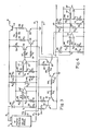
- FIG. 3 A circuit diagram of a preferred embodiment for turn-on circuit 15 is illustrated in Fig. 3.
- a Darlington PNP power transistor 31 has an emitter-collector path connected in series between the terminals. Power is selectively coupled between terminals 13 and 17 by the emitter-collector path of PNP Darlington power transistor 32.
- base electrodes for transistors 31 and 32 are selectively forward and reverse biased to close and open the series switches formed by the emitter-collector paths of the Darlington transistors.
- the emitter-collector path of transistor 32 is rendered into a conducting state in response to a lower voltage between terminals 12 and 14 than is required to provide a low impedance emitter-collector path for transistor 31.
- the path from terminals 13 and 14 to resistor 34 is interrupted so that the power supplied by panel 11 and dissipated by the resistor is available to be transferred by transistor 32 to terminal 17.
- the shunt path through resistor 33 is open circuited and the power dissipated by resistor 33 is available to be coupled through transistor 31 to terminal 16 and thence to inverter 28 and load 25.
- resistors 33 and 34 load power supply terminals 12 and 13, the output power of the supply is less than immediately after transistors 31 and 33 are activated to the forward biased condition. Such a result is achieved by selecting resistors 33 and 34 so that the panel output voltage is less than the maximum power point, e.g., along portion 22 of curve 18.
- inverter 28 is opened so the output of panel 11 is at the maximum power point, e.g., point 23, whereby the panel- output voltage increases.
- resistors 33 and 34 are decoupled from solar panel 11, the panel voltage jumps providing a hysteresis effect. Such an effect occurs because the incident radiation on panel 11 must decrease or the panel temperature must increase by an amount sufficient to reduce the panel output voltage below the same threshold value which originally caused the system to switch transistor 31 into a conducting state.
- Zener diodes 35 and 36 To control switching the transistors 31 and 32 and selective loading of panel 11 by resistors 33 and 34, Zener diodes 35 and 36, and d.c. operational amplifiers 37 and 38' are provided. Zener diodes 35 and 36 are respectively connected in series with resistors 38 and 39. Each of the series combinations of Zener diode 35 and resistor 38 and Zener diode 36 and resistor 39 is connected in a separate branch circuit shunting terminals 12 and 14 of solar panel 11. Zener diodes 35 and 36 have different threshold voltages, V Z1 and V Z3 , with the value of V z1 being greater than V Z3 in the preferred embodiment.
- the branch circuit including Zener diode 36 and resistor 39 remains in a non-conducting state for a lower voltage range than the branch circuit comprising Zener diode 35 and resistor 38.
- current respectively flows through resistors 38 and 39, and there are corresponding increases in the voltages developed across these resistors from a zero level to (V, - V z i) and (V S - V z3 ), where V s is the d.c. voltage derived by panel 11 and supplied to terminal 12.
- the voltages developed across resistors 38 and 39 are compared with reference voltages respectively developed across resistors 41 and 42.
- the comparisons are performed by differential non-feedback operational amplifiers 37 and 38' having bi-level outputs such that the output of each amplifier is a predetermined negative d.c. voltage in response to the voltage applied to the inverting input terminal of the amplifier being greater than the voltage applied to the non-inverting input terminal of the amplifier; in response to the voltage applied to the non-inverting input terminal being greater than the voltage applied to the inverting input terminal of the amplifier, the amplifier derives a predetermined positive d.c. output voltage.
- resistors 41 and 42 The voltages applied to resistors 41 and 42 and stabilized by a voltage regulator comprising resistor 43 and Zener diode 44, connected in series across terminals 12 and 14 of solar panel 11.
- a regulated d.c. voltage developed between the anode and cathode of Zener diode 44 is respectively applied to resistors 41 and 42 by resistors 45 and 46. Taps between resistors 41 and 45 and between resistors 42 and 46 are respectively connected to non-inverting and inverting input terminals of amplifiers 37 and 38.
- the inverting and non-inverting input terminals of amplifiers 37 and 38 are respectively connected to be responsive to the voltages developed across resistors 38 and 39; the voltages developed across the resistors are respectively coupled to the inverting and non-inverting input terminals of amplifiers 37 and 38' by resistors 47 and 48.
- D.C. power supply terminals of amplifiers 37 and 38 are connected to be energized by the regulated voltage between the anode and cathode of Zener diode 44.
- the values of resistors 38, 41, 45 and 47 are selected to provide the desired threshold characteristics of amplifier 37 in response to the threshold voltage of Zener diode 35.
- the values of resistors 39, 42, 46 and 48 are selected to provide the desired transitional characteristics for the output of amplifier 38, as a function of the threshold voltage of Zener diode 36.
- the bi-level output of amplifier 37 controls the switching of transistors 31, 52, 55, and 58 and therefore the selective connection of resistor 33 in shunt with terminals 12 and 14.
- the output of amplifier 37 is coupled through current limiting resistor 51 to the base of NPN transistor 52, having an emitter-collector path in shunt with terminals 12 and 14.
- the collector of transistor 52 is connected to load resistor 53, in turn connected to resistor 54 that shunts the emitter-base path of Darlington switching transistor 31.
- the collector of transistor 52 is connected in d.c. circuit with the base of NPN transistor 55, having an emitter connected directly to terminal 14 and a collector connected through resistor 56 to the base of transistor 31.
- the output voltage of amplifier 37 is coupled by resistor 57 to the base of Darlington NPN power transistor 58 having an emitter-collector path that selectively connects resistor 33 as a load for terminals 12 and 14.
- Transistor 58 is connected in a common emitter mode, whereby the transistor emitter is connected to terminal 14 and the transistor collector is connected to one terminal of resistor 33, the other terminal of which is connected directly to terminal 12.
- transistor 31 While transistor 58 is forward biased, transistor 31 is back biased because the positive voltage at the output of amplifier 37 forward biases transistor 52, which in turn back biases transistor 55.
- the back bias of transistor 55 prevents the flow of substantial negative current to the base of transistor 31, to cut off the emitter-collector path of transistor 31.
- transistor 31 is turned on, and the power formerly dissipated in resistor 33 is available to be transferred through the emitter-collector path of transistor 31 to terminal 16.
- Resistor 34 and transistor 32 are switched in response to the output of amplifier 38' in a manner somewhat similar to switching oftransis- tor 31 and resistor 33.
- amplifier 38 In response to the output voltage of solar panel 11 being less than the threshold of Zener diode 36, amplifier 38 provides an output voltage of zero volt d.c. which back biases common emitter NPN transistors 61 and 62 into a cut off state, by virtue of the connection of the bases of these transistors to the output of amplifier 38 through current limiting resistors 63 and 64, respectively.
- the collector of transistor 61 is connected to intermediate tap 13 of panel 11 by load resistor 65, across which is developed a voltage which is applied to the base of PNP Darlington power transistor 66.
- the emitter-collector path of transistor 66 is activated into a conducting state in response to the voltage across resistor 65, whereby dummy load resistor 34 is connected in shunt between terminals 13 and 14 of panel 11. Simultaneously, transistor 32 is rendered into a cut off condition because the high impedance state of the emitter-collector path of transistor 62 causes the base-emitter junction of transistor 32 to be back biased, preventing current flow therein.
- resistor 68 is connected between transistor 62 and the base of power transistor 32.
- the output of amplifier 38 jumps to a positive value which forward biases transistors 61 and 62.
- transistor 61 and 62 being forward biased, the base-emitter junctions of transistors 66 and 32 are respectively back and forward biased, in response to transistor 66 being back biased, the power dissipated by resistor 34 connected between terminals 13 and 14 of solar panel 11 is turned off and this power, derived from the panel output terminal 13, is available to be supplied to the load at terminal 17; the load is now coupled to terminal 13 by way of the emitter-collector path of forward biased transistor 32.
- the load connected to terminal 17 comprises the control circuitry for inverter 28, namely maximum power point sensor 26 and function generator 27.
- the value of resistor 34 is selected so that the output of panel 11 is along the relatively high negative slope portion 22 of the panel characteristic curve 18.
- the value of resistor 34 should be selected to be as close as possible to maximum power point 23 for the minimum open circuit output voltage of the panel that is to be coupled to terminal 17. Since the load connected to terminal 17 is relatively constant, being logic control circuitry, rather than a variable, high power consuming load such as a motor, and because the voltage between terminals 13 and 14 is considerably less than the voltage between the terminals 12 and 14, it is easier to select the value of resistor 34 to be close to a maximum power point than is the case for the voltage between terminals 12 and 14.
- Zener diode 36 Because the threshold voltage of Zener diode 36 is less than the threshold voltage of Zener diode 35, power is supplied to terminal 17 prior to power being applied to terminal 16, as the amount of solar energy incident on panel 11 increases. Therefore, maximum power point sensor 26, function generator 27 and inverter 28 receive power and are in an operational condition prior to power being applied to the inverter by terminal 16, to provide an orderly relatively low transient transfer of power from panel 11 to load 25.
- Zener diode 35 is activated into a cut off condition prior to Zener diode 36 being cut off.
- Fig. 3 the circuit of Fig. 3 is modified as indicated in Fig. 4.
- the anodes of Zener diodes 35 and 36 are connected together, and the diodes are selected so the thresholds are as close as possible to each other.
- the voltages acres: resistors 38 and 39 simultaneously jump from a zero to a finite value as the amount of solar energy incident on panel 11 increases.
- the voltages across resistors 38 and 39 simultaneously varyfrom a positive to a zero value.
- resistors 33 and 34 are simultaneously connected in shunt with and are decoupled from terminals 12 and 13, and transistors 31 and 32 are simultaneously activated and deactivated into a conducting and non-conducting state.
- resistors 33 and 34 in the former cause solar panel 11 to operate along high slope segment 22 at the time the amount of incident energy on the solar panel causes the voltages across resistors 38 and 39 to jump from zero to a finite level.
- an indication of the incident solar energy on panel 11 can be derived by monitoring the output current of the panel and comparing it with a reference.
- the values of dummy loads 33 and 34 are selected so that the load line intersects portion 21 of curve 18 having a slope less than one.
Landscapes
- Engineering & Computer Science (AREA)
- Electromagnetism (AREA)
- Sustainable Development (AREA)
- Sustainable Energy (AREA)
- Power Engineering (AREA)
- Physics & Mathematics (AREA)
- Life Sciences & Earth Sciences (AREA)
- General Physics & Mathematics (AREA)
- Radar, Positioning & Navigation (AREA)
- Automation & Control Theory (AREA)
- Control Of Electrical Variables (AREA)
- Photovoltaic Devices (AREA)
- Direct Current Feeding And Distribution (AREA)
Description
- The present invention relates generally to a system and circuit for controlling the power applied by a photovoltaic solar panel d.c. source to a load, and, in preferred embodiments of the invention, to such a system and circuit wherein a series switch between the panel and the load is selectively opened and closed in response to the voltage level derived from the panel.
- The voltage derived from a photovoltaic solar panel d.c. source is a function of the sunlight incident on the panel and the temperature of the panel. Therefore, the voltage derived from the panel is highly variable due to the long and short term variations of solar energy incident on the panel. The available power per unit area of the solar panel goes from a nocturnal value of zero to a maximum value at the middle of a sunny day. The power derived from the panel may have a relatively constant value during the entire daytime hours on hazy days. The power derived from the panel can also have sudden variations due to clouds transiently in the field of view of the panel to the sun.
- Solar panel systems are presently being designed wherein a load is driven directly by the panel output voltage without the intermediary of an energy storage device, such as a rechargeable battery. Such systems usually include, for efficient operation, a chopping d.c. to a.c. inverter, with associated control circuitry. One particularly advantageous chopper is disclosed in U.S. Patent 4,135,235, wherein a pseudo-sinusoidal, notched, multilevel waveform is derived from a d.c. source and supplied to an a.c load, such as a synchronous motor. This inverter, preferably controlled by a variable frequency function generator as disclosed in U.S. Patent 4,167,775, is such that the power output and current supplied from the d.c. source to the a.c. load increase proportionately with fundamental chopping frequency of the inverter. It is desired to supply maximum power from the panel to the inverter and to a load. However, the maximum power which can be derived from the panel is variable, as indicated above.
- For any particular incident solar energy level at a given temperature, the output power of the panel is a function of the panel load, which in turn controls the panel output voltage and current. The output of a photovoltaic solar panel can thus be represented as a family of curves for the panel voltage versus current output parameters. The open circuit voltage and short circuit current of each curve in the family both increases when the level of the incident solar energy on a panel increases for a given temperature. Each of the curves has a point corresponding to maximum power, at which the curve has a slope of minus one. Each of the curves has slopes with absolute values greater than one and less than one for currents respectively greater than and less than the maximum power point.
- Equipment to track the maximum available power from the panel and to control the chopping frequency of the inverter in response thereto must be shut down in an orderly fashion when the available power from the solar panel is reduced below some minimum value necessary to maintain control of the inverter. Also, in day-night ar"; night-day transitions, it is necessary to remove power from the inverter and control circuitry and supply power to the control circuitry and inverter in an orderly manner, while always ensuring that sufficient control power exists to meet stability requirements of the inverter and the load.
- In U.S. Patent 3,488,575, there is disclosed a solar energy system having a switch arranged in circuit between the solar cell and its load for disconnecting the cell from the load in the absence of sufficient light falling on the cell. The switch is a reed switch having a winding which is energised by the output voltage of the solar cell. Providing the cell output voltage exceeds a given level, the electromagnetic field generated by the winding is sufficient to hold the reed switch closed. However, the winding is permanently energised and so is always consuming energy produced by the solar cell which is wasteful. Furthermore, opening and closing of the reed switch takes place at a given solar cell output voltage so that if the cell output fluctuates at around the threshold level, the cell will be successively connected and disconnected to the load which is disadvantageous.
- French Patent 2,175,653 discloses a fairly complex control circuit which connects part of the cell output to a storage battery when the cell output power exceeds the power requirement of the load, but, when the cell output falls below that required by the load, the cell is disconnected from the battery and the battery re-connected to the load to boost the power supplied to it from the cell. The system uses a mode detector whose function is to control operation of the required switching as between the solar cell, battery and load according to a comparison between the cell output power and the power requirement of the load. The mode detector has a controllable hysteresis range. Therefore, small fluctuations in solar cell output power around the lower power requirement and within the hysteresis range will not result in the circuitry continually switching one way and then the other. However, it will be appreciated that the hysteresis effect displayed by the mode detector is an in-built design characteristic of the mode detector itself.
- According to the present invention from one aspect, there is provided a solar energy system comprising a photovoltaic solar DC source; a load; control circuitry, including a maximum power point tracker, arranged to transfer the output power of the solar source to the load such that the solar DC source is maintained operating substantially at the point corresponding to maximum power on its output voltage-versus-current characteristic, characterised by a turn-on circuit between the output of the solar source and the input to the control circuitry, said turn-on circuit being arranged to provide no output when an output parameter of the solar source is below a predetermined threshold level but to turn-on, to feed the output of the solar source through to the load via the control circuitry, when said predetermined threshold level is exceeded, the turn-on circuit comprising a first series switch between the solar source and said control circuitry, for selectively supplying voltage having one level to the load, a dummy load arranged in a branch circuit in shunt with the solar source, said branch circuit including a switch in said branch circuit, such that while said output parameter of said solar source is below said predetermined threshold level, said series switch is open but said further switch is closed, whereby power from said source is dissipated in the dummy load, and such that while said predetermined threshold level is exceeded, said further switch opens but said series switch closes whereby the dissipated power in the dummy load is now available to be supplied through the series switch.
- According to the invention from a further aspect, there is provided a method of controlling the application of d.c output power of a photovoltaic solar source to a load, comprising comparing an output parameter of the solar source with a predetermined threshold level, selectively controlling the coupling of power from the solar source either through a dummy load arranged in a branch circuit in shunt with the solar source or through the load itself according to the comparison result, such that while the output parameter of said source is below said predetermined level, the source power is coupled through the dummy load to be dissipated therein and no power is available for coupling through to the load, but while said predetermined value is exceeded, the source power is coupled through to the load whereby the power dissipated in the dummy load is now available for supply to the load, the coupling of power through to the load being via control circuitry, including a maximum power point tracker, such that the source power, when coupled through to the load, is controlled so as to maintain the solar source operating substantially at the point corresponding to maximum power on its output voltage-versus-current characteristics.
- Accordingly, while the output power of the solar source is being supplied to the main load, no energy is being dissipated in the dummy load. Furthermore, as will be described in detail herein below with reference to the accompanying drawings, this solar energy system, due to the particular shape that the output voltage-versus-current characteristics of the solar energy system has, will operate with a hysteresis effect, without the need for any special in-built circuit elements for achieving this result.
- Embodiments of the present invention provide a new and improved circuit and system for providing orderly control of the power applied by a photovoltaic solar panel d.c. source to a load despite varying long and short term solar conditions of the panel. Such embodiments may include an inverter in the control circuitry which transfers the output power of the solar energy source to the load, the inverter having a chopping frequency controlled so that maximum available power from the panel is supplied to the inverter and orderly control for the turn-on and turn-off of the inverter and control circuitry thereof is provided.
- In accordance with a preferred embodiment of the present invention, a system for providing orderly control of the power applied by a photovoltaic solar panel d.c. source to a load comprises means for coupling power from the panel to an inverter that drives the load and for preventing the coupling of power from the panel to the inverter in response to the voltage level of the panel being respectively greater than a predetermined value and less than a predetermined value. The coupling means is utilised in combination with an inverter control circuit that is responsive to the voltage from the source to control the switching frequency of the inverter so that substantially maximum power is supplied by the panel to the inverter for the incident solar energy and temperature of the panel. The inverter control circuit requires appreciably less power than the load and includes an input power supply terminal that is selectively connected to the output of the photovoltaic solar panel d.c. source. The control circuit power supply terminal is selectively connected to the panel so that power is coupled to the terminal or decoupled from the terminal depending upon the voltage derived from the panel.
- To prevent short term solar conditions of the panel which result in relatively short transitory fluctuations of the panel output voltage from adversely affecting the performance of the inverter and control circuitry for the inverter, the coupling of power to the inverter and the control circuitry is provided with voltage hysteresis. Thereby, in order to change the state of a switch that couples power from the panel to the inverter and a second switch which couples power from the panel to the control circuitry, the panel voltage must drop below a level that initially causes the switches to be activated into a conducting state. The hysteresis is provided by a pair of dummy loads that are connected in a shunt with the panel only while the switches are in a cut-off condition. While the dummy loads are connected in shunt with panels, they reduce the output voltage of the panel until the panel is responsive to a predetermined level of solar energy at a particular temperature. In response to the panel responding to the predetermined amount of solar energy, at the particular temperature, the switches are activated and the dummy loads are disconnected from the panel. Thereby, power is available from the panel which can be applied to the inverter and an actual load, rather than to the dummy loads. Disconnecting the dummy loads from the panel enables the panel voltage to increase above a threshold value at which the switches connected to the inverter and the inverter control circuitry are activated to a closed condition. These switches are not returned to an open circuit condition until the panel voltage drops below the threshold value. Hence a determination is made as to whether a panel output parameter value is above or below a predetermined threshold. In response tn the output parameter value below belong the threshold, the panel is loaded with an impedance that causes the panel to derive the output parameter with a value different from the parameter value at the maximum power point for the panel at the threshold while the panel is decoupled from the load. In response to the output parameter being above the threshold, the panel is coupled to the load while the panel is operated substantially at the maximum power.
- The hysteresis effect relies upon the family of curves for the voltage versus current output parameters of the panels. In particular, the power supplied by the panel to the load is controlled by monitoring one of the output parameters (voltage or current) of the panel to indicate whether the solar energy incident on the panel is above or below a reference value. In the particular embodiment described in detail, the parameter is the output voltage of the panel, although it is to be understood that the output current of the panel can also be monitored. Also, the reference value is proportional to the panel d.c. output voltage. In response to the parameter indicating that the incident energy is below the threshold, the dummy load is connected to the panel, and the series switch between the panel and the load is open circuited, to prevent the coupling .power from the panel to the load: In the particular embodiment, the dummy load causes the panel to operate along the portion of the curve having a slope greater than one. If, however, current is monitored, the dummy load causes the panel to operate along the portion of the curve where the slope of the curve is less than one. In any event, the dummy load causes the output power of the panel to differ from the panel maximum power at the threshold value of the incident energy. In response to the parameter indicating that the incident energy is above the threshold, the dummy load is disconnected from the panel. Simultaneously, power from the panel is coupled to the load. The current or voltage supplied to the load is then adjusted so that maximum power is supplied by the panel to the load. Because the maximum power point is at a panel voltage above the panel voltage which causes the dummy load to be connected in circuit or is less than the current which causes the dummy load to be connected in the circuit, hysteresis is automatically provided by controlling the inverter so it has a chopping frequency which causes maximum power to be supplied to the load and by judicious selection of the magnitude of the dummy loads.
- The above and still further objects, features and advantages of the present invention and embodiment thereof will become apparent upon consideration of the following detailed description of several specific embodiments thereof, given by way of example, especially when taken in conjunction with the accompanying drawings in which:
- Figure 1 is a system block diagram of one preferred embodiment of the invention;
- Figure 2 are curves indicating the voltage- current characteristics of the output of a solar panel illustrated in Fig. 1 for two particular levels of incident solar energy and temperature;
- Figure 3 is a circuit diagram of the automatic turn-on circuit illustrated in Fig. 1, in accordance with one embodiment; and
- Figure 4 is a circuit diagram of a portion of a modified version of the automatic turn-on circuit.
- Reference is now made to Fig. 1 of the drawings wherein a silicon photovoltaic solar panel 11 is illustrated as including a high
voltage output terminal 12, anintermediate output terminal 13, and aground terminal 14. The d.c. voltage developed by solar panel 11 atterminals terminals terminal 14. - The voltages at
terminals circuit 15, described in detail in different embodiments, in connection with Figs. 3 and 4.Circuit 15 responds to the voltage atterminal 12 to selectively couple the voltages atterminals output terminals 16 and 17. In one embodiment, the voltages atterminals terminals 16 and 17 by separate series switches in turn-oncircuit 15 in response to the voltage atterminal 12 exceeding a single predetermined value. In a second embodiment, the voltages atterminals terminals 16 and 17 in response to the voltage atterminal 12 having two different values. If the latter embodiment is employed, it is generally preferable for the voltage atterminal 13 to be supplied to terminal 17 in response to the voltage atterminal 12 having a somewhat lower value than is required to enable the voltage atterminal 12 to be coupled toterminal 16. In both embodiments, the two series switches incircuit 15 betweenterminals terminals 13 and 17 have voltage hysteresis characteristics. Thereby,terminals terminals 13 and 17 are connected to each other in response to the voltage atterminal 12 exceeding a threshold value V, (for the single threshold situation) or Vt1 and Vt2 (for the situation of separate thresholds) by a predetermined value, ΔV.Terminals terminals 13 and 17 remain connected together until the voltage atterminal 12 drops below the threshold value. Thereby, relatively high frequency transient variations in the output voltage and power of solar panel 11, as occur in response to clouds, passing aircraft, and debris being in the field of view between the solar panel and the sun, do not cause the switches incircuit 15 to change state once the switches are activated into a conducting state. - For any particular temperature and incident solar energy condition of solar panel 11, the solar panel has a predetermined voltage versus current characteristic.
Curve 18, Fig. 2, is an illustration of the voltage versus current characteristic of solar panel 11 for one particular temperature and incident solar energy situation.Curve 18 has a maximum voltage value (V = Vco) and zero current value (I = 0) atpoint 19 when no load is connected across thesolar panel terminals terminals point 20 oncurve 18.Curve 18 includes afirst portion 21 having a negative slope less than one extending frompoint 19 to the point corresponding tomaximum power 23 and asecond portion 22 having a negative slope greater than one betweenpoints Portions maximum power point 23 where the slope is minus one and the product of the output voltage and current of panel 11 is a maximum. It is desirable to maintain the voltages supplied by panel 11 to a load at themaximum power point 23. For differing temperatures and incident solar energy conditions of panel 11, the position ofpoint 23 varies. - To enable panel 11 to provide maximum power to load 25, typically an inductive load such as a synchronous motor, the voltage to output terminal 17 of
circuit 15 is sampled by maximumpower point sensor 26. In response to the output voltage ofcircuit 15 at terminal 17,sensor 26 derives a d.c. voltage which is applied tofunction generator 27, preferably of the type illustrated in the previously mentioned U.S. Patent No. 4,167,775.Function generator 27 responds to the d.c. output ofsensor 26 to provide a variable frequency input topower inverter 28 that chops the d.c. voltage atterminal 16 into a multi-level, notched pseudo sinusoidal squarewave that is applied to load 25. In one preferred embodiment,inverter 28 is of the type illustrated in the previously mentioned U.S. Patent No. 4,135,235. In one preferred embodiment, maximumpower point sensor 26 is of the type described and illustrated in my copending, commonly assigned application EP-80 304237.3 entitled "Solar Power Automatic Maximum Power Tracking System", published on 03-06-81 under the number EP-A,-0029743. - Maximum power is transferred between panel 11 and
load 25 by utilisingsensor 26,function generator 27, andinverter 28.Inverter 28 drivesmotor load 25, having a constant volts per Hertz ratio, so the power and current supplied by panel 11 toinverter 28 are linearly proportional to the chopping frequency of the fundamental of the pseudo sinusoidal wave derived by the inverter. Because the maximum power available from panel 11, as determined bysensor 26, controls the fundamental frequency offunction generator 27 and therefore the fundamental output frequency ofinverter 28, the electric power transferred from panel 11 to load 25 is automatically maximized. Because the power supplied by panel 11 throughcircuit 15 toinverter 28 is linearly proportional to the fundamental chopping frequency of the inverter the inverter fundamental chopping frequency determines the amount of power and current drawn by the inverter and load from panel 11. Increasing the fundamental chopping frequency ofinverter 28 therefore increases the power and current drawn from the solar panel; decreasing the fundamental chopping frequency ofinverter 28 decreases the power and current drawn from the solar panel. Maximumpower point sensor 26 controls the frequency supplied bygenerator 27 toinverter 28 in such a way that the voltage and current supplied by the panel to the input ofinverter 28 are approximately atmaximum power point 23. At the maximum power point, the fundamental chopping frequency ofinverter 28 is stabilized. In response to the current supplied to load 25 being above and below the maximum power point, the fundamental chopping frequency is respectively above and below the stabilized chopping frequency. - Maximum
power point sensor 26 andfunction generator 27 include relatively low power logic circuitry, powered by the output of panel 11. D.C. Power supplies in logic circuitry ofsensor 26 andfunction generator 27 are typically at relatively low voltage values and therefore are derived fromintermediate output terminal 13 of panel 11, as selectively coupled through turn-oncircuit 15 to terminal 17. In one embodiment, the power supply voltage developed at terminal 17 energizes the logic circuitry withinsensor 26 andfunction generator 27 prior to power being supplied bycircuit 15 to the high power,high voltage output 16. Thereby,sensor 26 andfunction generator 27 are deriving output voltages at the time power is applied toterminal 16. Hence, transients in the output offunction generator 27 are minimized when power is applied toterminal 16 and there is an orderly transfer of power, with a minimum of transients, when terminal 16 begins to supplyload 25. - A circuit diagram of a preferred embodiment for turn-on
circuit 15 is illustrated in Fig. 3. To selectively couple power betweenterminals terminals 13 and 17 by the emitter-collector path of PNPDarlington power transistor 32. In response to the magnitude of the voltage derived by solar panel 11 betweenterminals transistors 31 and 32 are selectively forward and reverse biased to close and open the series switches formed by the emitter-collector paths of the Darlington transistors. In the embodiment of Fig. 3, the emitter-collector path oftransistor 32 is rendered into a conducting state in response to a lower voltage betweenterminals - While the emitter-collector path for
transistors 31 and 32 are cut-off, dummy loads, includingresistors 33 and 34, are respectively connected in shunt withterminals PNP transistor 32 being activated into the conducting state, the path fromterminals resistor 34 is interrupted so that the power supplied by panel 11 and dissipated by the resistor is available to be transferred bytransistor 32 to terminal 17. Similarly, when the base emitter junction of transistor 31 is forward biased, the shunt path through resistor 33 is open circuited and the power dissipated by resistor 33 is available to be coupled through transistor 31 toterminal 16 and thence toinverter 28 andload 25. Whileresistors 33 and 34 loadpower supply terminals resistors 33 and 34 so that the panel output voltage is less than the maximum power point, e.g., alongportion 22 ofcurve 18. When the maximumpower point sensor 26 is activated,inverter 28 is opened so the output of panel 11 is at the maximum power point, e.g.,point 23, whereby the panel- output voltage increases. Whenresistors 33 and 34 are decoupled from solar panel 11, the panel voltage jumps providing a hysteresis effect. Such an effect occurs because the incident radiation on panel 11 must decrease or the panel temperature must increase by an amount sufficient to reduce the panel output voltage below the same threshold value which originally caused the system to switch transistor 31 into a conducting state. - To control switching the
transistors 31 and 32 and selective loading of panel 11 byresistors 33 and 34,Zener diodes operational amplifiers 37 and 38' are provided.Zener diodes resistors Zener diode 35 andresistor 38 andZener diode 36 andresistor 39 is connected in a separate branchcircuit shunting terminals Zener diodes Zener diode 36 andresistor 39 remains in a non-conducting state for a lower voltage range than the branch circuit comprisingZener diode 35 andresistor 38. In response to the threshold voltages ofZener diodes resistors terminal 12. - The voltages developed across
resistors resistors operational amplifiers 37 and 38' having bi-level outputs such that the output of each amplifier is a predetermined negative d.c. voltage in response to the voltage applied to the inverting input terminal of the amplifier being greater than the voltage applied to the non-inverting input terminal of the amplifier; in response to the voltage applied to the non-inverting input terminal being greater than the voltage applied to the inverting input terminal of the amplifier, the amplifier derives a predetermined positive d.c. output voltage. The voltages applied toresistors regulator comprising resistor 43 and Zener diode 44, connected in series acrossterminals resistors resistors resistors resistors amplifiers amplifiers resistors amplifiers 37 and 38' byresistors amplifiers resistors amplifier 37 in response to the threshold voltage ofZener diode 35. Similarly, the values ofresistors amplifier 38, as a function of the threshold voltage ofZener diode 36. - The bi-level output of
amplifier 37 controls the switching oftransistors terminals amplifier 37 is coupled through current limitingresistor 51 to the base ofNPN transistor 52, having an emitter-collector path in shunt withterminals transistor 52 is connected to loadresistor 53, in turn connected toresistor 54 that shunts the emitter-base path of Darlington switching transistor 31. The collector oftransistor 52 is connected in d.c. circuit with the base ofNPN transistor 55, having an emitter connected directly toterminal 14 and a collector connected throughresistor 56 to the base of transistor 31. The output voltage ofamplifier 37 is coupled byresistor 57 to the base of DarlingtonNPN power transistor 58 having an emitter-collector path that selectively connects resistor 33 as a load forterminals Transistor 58 is connected in a common emitter mode, whereby the transistor emitter is connected toterminal 14 and the transistor collector is connected to one terminal of resistor 33, the other terminal of which is connected directly toterminal 12. - In response to the voltage at
terminal 12 being less than the threshold voltage ofZener diode 35, no current flows throughresistor 38 and substantially zero voltage is applied to the inverting input ofamplifier 37, wnereby a positive d.c. voltage is derived at the amplifier output. A positive d.c. voltage at the output ofamplifier 37forward biases transistor 58, to connect resistor 33 acrossterminals Zener diode 35 are selected so that panel 11 operates alongsegment 22 whiletransistor 58 is in a forward biased condition and a voltage less than the threshold voltage ofZener diode 35 is developed betweenterminals - While
transistor 58 is forward biased, transistor 31 is back biased because the positive voltage at the output ofamplifier 37forward biases transistor 52, which in turn backbiases transistor 55. The back bias oftransistor 55 prevents the flow of substantial negative current to the base of transistor 31, to cut off the emitter-collector path of transistor 31. - When the voltage derived by panel 11 is slightly less than the threshold voltage of
Zener diode 35, the power from the panel dissipated in resistor 33 equals approximately (V,,,)'/R2, where R2 equals the value of resistor 33. In response to the voltage of panel 11 reaching and exceeding the threshold voltage ofZener diode 35, this diode conducts current causing Va to exceed Vb in amplitude, in turn causing the sequence ofamplifier 37 changing its output voltage to a zero level, turning offtransistors transistor 52 so turns off, the voltage at its collector is raised towards +Vs, causing the base emitter junction oftransistor 55 to be forward biased turning the latter on. Base emitter current now flows from transistor 31 throughresistor 56 and the collector-emitter path oftransistor 55, to a source of reference potential, ground in this example. As a result, transistor 31 is turned on, and the power formerly dissipated in resistor 33 is available to be transferred through the emitter-collector path of transistor 31 toterminal 16. Hence, there is not a very large shift in the power requirements of panel 11 at the time transistor 31 is switched from a cut off to a conducting state, resulting in relatively smooth operation ofsensor 26,function generator 27 andinverter 28, at the time the inverter is supplied with d.c. power byterminal 16. -
Resistor 34 andtransistor 32 are switched in response to the output of amplifier 38' in a manner somewhat similar to switching oftransis- tor 31 and resistor 33. In response to the output voltage of solar panel 11 being less than the threshold ofZener diode 36,amplifier 38 provides an output voltage of zero volt d.c. which back biases commonemitter NPN transistors amplifier 38 through current limitingresistors transistor 61 is connected tointermediate tap 13 of panel 11 byload resistor 65, across which is developed a voltage which is applied to the base of PNPDarlington power transistor 66. The emitter-collector path oftransistor 66 is activated into a conducting state in response to the voltage acrossresistor 65, wherebydummy load resistor 34 is connected in shunt betweenterminals transistor 32 is rendered into a cut off condition because the high impedance state of the emitter-collector path oftransistor 62 causes the base-emitter junction oftransistor 32 to be back biased, preventing current flow therein. To provide an appropriate load for the emitter-collector path oftransistor 62 when the transistor is activated into a conducting state,resistor 68 is connected betweentransistor 62 and the base ofpower transistor 32. - In response to the voltage of solar panel 11 reaching or exceeding the threshold of
Zener diode 36, the output ofamplifier 38 jumps to a positive value whichforward biases transistors transistor transistors transistor 66 being back biased, the power dissipated byresistor 34 connected betweenterminals panel output terminal 13, is available to be supplied to the load at terminal 17; the load is now coupled toterminal 13 by way of the emitter-collector path of forward biasedtransistor 32. The load connected to terminal 17 comprises the control circuitry forinverter 28, namely maximumpower point sensor 26 andfunction generator 27. The value ofresistor 34 is selected so that the output of panel 11 is along the relatively highnegative slope portion 22 of the panelcharacteristic curve 18. However, the value ofresistor 34 should be selected to be as close as possible tomaximum power point 23 for the minimum open circuit output voltage of the panel that is to be coupled to terminal 17. Since the load connected to terminal 17 is relatively constant, being logic control circuitry, rather than a variable, high power consuming load such as a motor, and because the voltage betweenterminals terminals resistor 34 to be close to a maximum power point than is the case for the voltage betweenterminals - Because the threshold voltage of
Zener diode 36 is less than the threshold voltage ofZener diode 35, power is supplied to terminal 17 prior to power being applied toterminal 16, as the amount of solar energy incident on panel 11 increases. Therefore, maximumpower point sensor 26,function generator 27 andinverter 28 receive power and are in an operational condition prior to power being applied to the inverter byterminal 16, to provide an orderly relatively low transient transfer of power from panel 11 to load 25. - Similarly, as the amount of energy incident on panel 11 decreases,
Zener diode 35 is activated into a cut off condition prior toZener diode 36 being cut off. The presence of maximumpower point sensor 26 and the proper selection of the values ofresistors 33 and 34, however, provide for the hysteresis effect, wherebyZener diode 35 is switched off in response to a lower intensity of solar energy incident on panel 11 than the intensity required to activate the Zener diode into a conducting state. - This result is seen from
curves Zener diode 35 is indicated by thehorizontal line 72, having a value of Vz1' Assume that panel 11 is illuminated so its output characteristic is indicated bycurve 18 and that transistor 31 is cut off. Also assume that the load of panel 11 comprises resistor 33 and the relatively constant load acrossterminals 17 and 14. Such a load is indicated byload line 73 which intersectsthreshold line 72 ofZener diode 35 onportion 22 ofcurve 18. Because the threshold voltage ofZener diode 35,load line 73 andcurve 18 coincide a slight increase in incident solar energy on panel 11 causes the threshold ofZener diode 35 to be exceeded, wherebytransistors 31 and 58 are respectively activated to conducting the cut off states. When transistor 31 conducts, maximum power point sensor-26 causes the load line to shift fromload line 73 toload line 74, which intersects maximum power point 23 -oncurve 18. The load line shift fromline 73 toline 74 results in an increased output voltage of panel 11, fromline 72 toline 75, a horizontal line intersectingmaximum power point 23. If there is a sudden, slight drop in the solar energy incident on panel 11 after the threshold ofZener diode 35 is reached, the output of panel 11 remains sufficiently high to maintaindiode 35 in a conducting state, whereby power continues to be applied to the load at terminal 16 through transistor switch 31. The threshold ofdiode 35 is exceeded until the solar energy incident on panel 11 is such that the panel output characteristic is indicated bycurve 71, having amaximum power point 76 at the intersecting threshold voltageline Zener diode 35. Because of the manner in which maximumpower point sensor 26 operates in connection withfunction generator 27 andinverter 28, the output voltage of panel 11 is determined by the loci of maximum power points for the family of panel current versus voltage curves. Becausemaximum power point 76 forcharacteristic curve 71 is lower than themaximum power point 23 forcurve 18, hysteresis for the operation of switching transistor 31 is automatically provided. - In accordance with another embodiment of the invention, power is simultaneously applied to
terminals 16 and 17. To this end, the circuit of Fig. 3 is modified as indicated in Fig. 4. In Fig. 4, the anodes ofZener diodes resistors resistors resistors resistors 33 and 34 are simultaneously connected in shunt with and are decoupled fromterminals transistors 31 and 32 are simultaneously activated and deactivated into a conducting and non-conducting state. Substantially the same hysteresis effect occurs with the system of Fig. 4 as in the system of Fig. 3 becauseresistors 33 and 34 in the former cause solar panel 11 to operate alonghigh slope segment 22 at the time the amount of incident energy on the solar panel causes the voltages acrossresistors - While there have been described and illustrated several specific embodiments of the invention, it will be clear that variations in the details of the embodiments specifically illustrated and described may be made without departing from the scope of the invention as defined in the appended claims. For example, an indication of the incident solar energy on panel 11 can be derived by monitoring the output current of the panel and comparing it with a reference. In such an instance, the values of dummy loads 33 and 34 are selected so that the load line intersects
portion 21 ofcurve 18 having a slope less than one.
Claims (7)
Applications Claiming Priority (2)
| Application Number | Priority Date | Filing Date | Title |
|---|---|---|---|
| US06/097,205 US4333136A (en) | 1979-11-26 | 1979-11-26 | Solar powered automatic turn-on control (SPA-TOC) unit and method |
| US97205 | 1998-06-12 |
Publications (2)
| Publication Number | Publication Date |
|---|---|
| EP0029744A1 EP0029744A1 (en) | 1981-06-03 |
| EP0029744B1 true EP0029744B1 (en) | 1985-05-02 |
Family
ID=22262036
Family Applications (1)
| Application Number | Title | Priority Date | Filing Date |
|---|---|---|---|
| EP19800304238 Expired EP0029744B1 (en) | 1979-11-26 | 1980-11-26 | Solar powered automatic turn-on control unit |
Country Status (6)
| Country | Link |
|---|---|
| US (1) | US4333136A (en) |
| EP (1) | EP0029744B1 (en) |
| JP (1) | JPS5686030A (en) |
| DE (1) | DE3070594D1 (en) |
| ES (1) | ES497109A0 (en) |
| ZA (1) | ZA807343B (en) |
Cited By (1)
| Publication number | Priority date | Publication date | Assignee | Title |
|---|---|---|---|---|
| CN111397077A (en) * | 2020-02-24 | 2020-07-10 | 珠海格力电器股份有限公司 | Temperature control method and device, storage medium and air conditioner |
Families Citing this family (40)
| Publication number | Priority date | Publication date | Assignee | Title |
|---|---|---|---|---|
| JPS5749328A (en) * | 1980-09-08 | 1982-03-23 | Fuji Electric Co Ltd | Control device for converter driven by solar battery |
| JPS58112422A (en) * | 1981-12-25 | 1983-07-04 | 株式会社荏原製作所 | Pump controller with solar battery as power source |
| JPS58168122A (en) * | 1982-03-30 | 1983-10-04 | Toshiba Corp | Operation processing device |
| US4489243A (en) * | 1982-05-06 | 1984-12-18 | The United States Of America As Represented By The Administrator Of The National Aeronautics And Space Administration | Solar powered actuator with continuously variable auxiliary power control |
| US4494180A (en) * | 1983-12-02 | 1985-01-15 | Franklin Electric Co., Inc. | Electrical power matching system |
| EP0231211A4 (en) * | 1985-07-11 | 1987-09-02 | Allan Russell Jones | Electronic control circuit. |
| JPS62293936A (en) * | 1986-06-11 | 1987-12-21 | 三菱電機株式会社 | Solar generator |
| PH25015A (en) * | 1986-12-19 | 1991-01-28 | Stuart Maxwell Watkins | Electrical power transfer apparatus |
| US5086267A (en) * | 1989-07-31 | 1992-02-04 | Intermatic Incorporated | Control circuit for a solar-powered rechargeable power source and load |
| US5041952A (en) * | 1989-07-31 | 1991-08-20 | Intermatic Incorporated | Control circuit for a solar-powered rechargeable power source and load |
| US5221891A (en) * | 1989-07-31 | 1993-06-22 | Intermatic Incorporated | Control circuit for a solar-powered rechargeable power source and load |
| US5204586A (en) * | 1991-07-17 | 1993-04-20 | Siemens Solar Industries, L.P. | Solar powered lamp having a circuit for providing positive turn-on at low light levels |
| US5592074A (en) * | 1992-06-26 | 1997-01-07 | Canon Kabushiki Kaisha | Battery power supply system |
| US5497312A (en) * | 1993-05-13 | 1996-03-05 | Toko America, Inc. | Drive signal controlled undervoltage lockout circuit |
| JPH09294334A (en) * | 1996-02-26 | 1997-11-11 | Sanyo Electric Co Ltd | Grid-connected generator |
| US5923100A (en) * | 1997-03-31 | 1999-07-13 | Lockheed Martin Corporation | Apparatus for controlling a solar array power system |
| US6291764B1 (en) * | 1999-03-24 | 2001-09-18 | Sanyo Electronics Co., Ltd. | Photovoltaic power generation device |
| US7269036B2 (en) * | 2003-05-12 | 2007-09-11 | Siemens Vdo Automotive Corporation | Method and apparatus for adjusting wakeup time in electrical power converter systems and transformer isolation |
| AU2005202869A1 (en) * | 2005-06-30 | 2007-01-18 | Tyco Projects (Australia) Pty Ltd | Switched dummy load for monitored AC loads |
| US20070290651A1 (en) * | 2006-06-14 | 2007-12-20 | Worldwater & Power Corp. | Solar power control using irradiance |
| TWI341349B (en) * | 2007-04-16 | 2011-05-01 | Asustek Comp Inc | Optoelectronic transformation structure and temperature control system using the same |
| US9407093B2 (en) | 2007-08-22 | 2016-08-02 | Maxout Renewables, Inc. | Method for balancing circuit voltage |
| US8625315B2 (en) * | 2008-05-09 | 2014-01-07 | Etm Electromatic Inc | Inverter modulator with variable switching frequency |
| US20110316609A1 (en) * | 2008-07-28 | 2011-12-29 | Ivus Industries, Llc | Bipolar junction transistor turn on-off power circuit |
| DE102008059428A1 (en) * | 2008-11-27 | 2010-06-10 | Diehl Ako Stiftung & Co. Kg | Energieeinspeisevorrichtung |
| US8791598B2 (en) * | 2008-12-21 | 2014-07-29 | NavSemi Energy Private Ltd. | System and method for selectively controlling a solar panel in segments |
| CN102460338B (en) | 2009-05-19 | 2014-08-13 | 最大输出可再生能源公司 | Construction of a power station comprising a cluster of power generating units |
| WO2011022381A2 (en) * | 2009-08-17 | 2011-02-24 | Navsemi Inc. | System and method for controlling a solar panel output |
| US9172312B2 (en) * | 2009-11-25 | 2015-10-27 | American Superconductor Corporation | Reducing photovoltaic array voltage during inverter re-enablement |
| CN102118043B (en) * | 2009-12-31 | 2013-12-04 | 比亚迪股份有限公司 | Solar charger for charging power battery |
| US8050062B2 (en) * | 2010-02-24 | 2011-11-01 | General Electric Company | Method and system to allow for high DC source voltage with lower DC link voltage in a two stage power converter |
| EP2564487A4 (en) | 2010-04-27 | 2015-10-28 | Navsemi Energy Private Ltd | Method and apparatus for controlling a solar panel output in charging a battery |
| DE102010017746A1 (en) * | 2010-05-03 | 2011-11-03 | Sma Solar Technology Ag | Method for limiting the generator voltage of a photovoltaic system in case of danger and photovoltaic system |
| US8395919B2 (en) * | 2010-07-29 | 2013-03-12 | General Electric Company | Photovoltaic inverter system and method of starting same at high open-circuit voltage |
| US8599586B2 (en) * | 2010-08-28 | 2013-12-03 | General Electric Company | Power inverter system and method of starting same at high DC voltage |
| WO2014149775A1 (en) * | 2013-03-15 | 2014-09-25 | Maxout Renewables, Inc. | Architecture for power plant comprising clusters of power-generation devices |
| CN105207506B (en) * | 2014-06-25 | 2017-12-29 | 华为技术有限公司 | A kind of control method of inverter, device and system |
| DE102015006608B4 (en) * | 2015-05-21 | 2018-11-15 | Audi Ag | Method for operating a photovoltaic device of a motor vehicle and motor vehicle |
| US11545931B2 (en) | 2019-11-10 | 2023-01-03 | Maxout Renewables, Inc. | Optimizing hybrid inverter system |
| CN117096851B (en) * | 2023-07-20 | 2024-06-25 | 上海正泰电源系统有限公司 | String photovoltaic array power prediction method, device and storage medium for inverter |
Family Cites Families (9)
| Publication number | Priority date | Publication date | Assignee | Title |
|---|---|---|---|---|
| US3648145A (en) * | 1970-05-08 | 1972-03-07 | Singer Co | Undervoltage protection device |
| DE2022942C3 (en) | 1970-05-12 | 1973-12-06 | Felten & Guilleaume Kabelwerke Ag, 5000 Koeln | Protection circuit to prevent deep discharge of an accumulator |
| US3740636A (en) * | 1971-11-05 | 1973-06-19 | Us Navy | Charge regulator and monitor for spacecraft solar cell/battery system control |
| FR2175653B1 (en) * | 1972-03-17 | 1977-04-01 | Labo Cent Telecommunicat | |
| GB1424383A (en) | 1973-08-11 | 1976-02-11 | Hawker Siddeley Dynamics Ltd | Tpower systems for spacecraft or orbiting satellites |
| US3919618A (en) * | 1974-06-10 | 1975-11-11 | Gates Rubber Co | Hysteresis battery charger |
| DE2433356A1 (en) | 1974-07-11 | 1976-01-22 | Ehmann Elektrotech | Battery charge state monitoring unit - has automatic load disconnection at preset voltage level |
| US4186336A (en) * | 1977-03-31 | 1980-01-29 | Organisation Europeenne De Recherches Spatiales | Limit cycling regulator apparatus for plural parallel power sources |
| US4204147A (en) * | 1977-08-04 | 1980-05-20 | Rca Corporation | Power transfer apparatus |
-
1979
- 1979-11-26 US US06/097,205 patent/US4333136A/en not_active Expired - Lifetime
-
1980
- 1980-11-25 ZA ZA00807343A patent/ZA807343B/en unknown
- 1980-11-25 ES ES497109A patent/ES497109A0/en active Granted
- 1980-11-26 JP JP16545580A patent/JPS5686030A/en active Pending
- 1980-11-26 EP EP19800304238 patent/EP0029744B1/en not_active Expired
- 1980-11-26 DE DE8080304238T patent/DE3070594D1/en not_active Expired
Cited By (2)
| Publication number | Priority date | Publication date | Assignee | Title |
|---|---|---|---|---|
| CN111397077A (en) * | 2020-02-24 | 2020-07-10 | 珠海格力电器股份有限公司 | Temperature control method and device, storage medium and air conditioner |
| CN111397077B (en) * | 2020-02-24 | 2021-03-23 | 珠海格力电器股份有限公司 | Temperature control method and device, storage medium and air conditioner |
Also Published As
| Publication number | Publication date |
|---|---|
| ZA807343B (en) | 1982-01-27 |
| EP0029744A1 (en) | 1981-06-03 |
| ES8202656A1 (en) | 1982-02-01 |
| US4333136A (en) | 1982-06-01 |
| DE3070594D1 (en) | 1985-06-05 |
| JPS5686030A (en) | 1981-07-13 |
| ES497109A0 (en) | 1982-02-01 |
Similar Documents
| Publication | Publication Date | Title |
|---|---|---|
| US4333136A (en) | Solar powered automatic turn-on control (SPA-TOC) unit and method | |
| US4742291A (en) | Interface control for storage battery based alternate energy systems | |
| US3919618A (en) | Hysteresis battery charger | |
| US3818307A (en) | Serially-connected converters having multiple regulation modes for use in supplying serially-connected loads on long lines | |
| US4044268A (en) | Multiple power source automatic switching circuitry | |
| US4335344A (en) | Voltage regulator for a controlled field generator | |
| US4678983A (en) | DC power supply with adjustable operating point | |
| US4277738A (en) | Generator voltage regulator | |
| US5073837A (en) | Low voltage protection circuit | |
| US4346337A (en) | Voltage regulator circuit with multiple control functions | |
| EP0137756A2 (en) | Motor vehicle electrical system | |
| US4611162A (en) | Parallel voltage regulators with different operating characteristics collectively forming a single regulator with wide operating range | |
| US9306082B2 (en) | System for managing and controlling photovoltaic panels | |
| US4306183A (en) | Voltage regulation circuit for a solar cell charging system | |
| KR980006706A (en) | A battery charge apparatus with mode-convertible function | |
| CA1226895A (en) | Photovoltaic power regulation system | |
| US3942096A (en) | Voltage regulating system | |
| US5153497A (en) | Circuit for regulating charging of a storage battery by a photovoltaic array | |
| EP0524466B1 (en) | A control device for an alternating current generator of a vehicle | |
| US4943761A (en) | Current limited DC power controller | |
| HK1002243B (en) | A control device for an alternating current generator of a vehicle | |
| CA1196952A (en) | Magneto alternator regulator with tachometer output | |
| US5341082A (en) | Reverse current flow protector for electricity storage systems | |
| US4286205A (en) | Interface circuit for standard voltage regulators | |
| US4342955A (en) | Voltage regulator for a fixed field A.C. generator |
Legal Events
| Date | Code | Title | Description |
|---|---|---|---|
| PUAI | Public reference made under article 153(3) epc to a published international application that has entered the european phase |
Free format text: ORIGINAL CODE: 0009012 |
|
| AK | Designated contracting states |
Designated state(s): DE FR GB IT |
|
| 17P | Request for examination filed |
Effective date: 19811022 |
|
| ITF | It: translation for a ep patent filed | ||
| RAP1 | Party data changed (applicant data changed or rights of an application transferred) |
Owner name: SOLAREX CORPORATION |
|
| GRAA | (expected) grant |
Free format text: ORIGINAL CODE: 0009210 |
|
| AK | Designated contracting states |
Designated state(s): DE FR GB IT |
|
| REF | Corresponds to: |
Ref document number: 3070594 Country of ref document: DE Date of ref document: 19850605 |
|
| ET | Fr: translation filed | ||
| PLBE | No opposition filed within time limit |
Free format text: ORIGINAL CODE: 0009261 |
|
| STAA | Information on the status of an ep patent application or granted ep patent |
Free format text: STATUS: NO OPPOSITION FILED WITHIN TIME LIMIT |
|
| 26N | No opposition filed | ||
| ITTA | It: last paid annual fee | ||
| PGFP | Annual fee paid to national office [announced via postgrant information from national office to epo] |
Ref country code: FR Payment date: 19920918 Year of fee payment: 13 |
|
| PGFP | Annual fee paid to national office [announced via postgrant information from national office to epo] |
Ref country code: GB Payment date: 19920923 Year of fee payment: 13 |
|
| PGFP | Annual fee paid to national office [announced via postgrant information from national office to epo] |
Ref country code: DE Payment date: 19921231 Year of fee payment: 13 |
|
| PG25 | Lapsed in a contracting state [announced via postgrant information from national office to epo] |
Ref country code: GB Effective date: 19931126 |
|
| GBPC | Gb: european patent ceased through non-payment of renewal fee |
Effective date: 19931126 |
|
| PG25 | Lapsed in a contracting state [announced via postgrant information from national office to epo] |
Ref country code: FR Effective date: 19940729 |
|
| PG25 | Lapsed in a contracting state [announced via postgrant information from national office to epo] |
Ref country code: DE Effective date: 19940802 |
|
| REG | Reference to a national code |
Ref country code: FR Ref legal event code: ST |